Table of Contents
Advertisement
Quick Links
One Technology Way • P.O. Box 9106 • Norwood, MA 02062-9106, U.S.A. • Tel: 781.329.4700 • Fax: 781.461.3113 • www.analog.com
FEATURES
Full-featured evaluation board for the AD9910
PC evaluation software for control and measurement of the
AD9910
USB interface
Graphic user interface (GUI) software with frequency sweep
capability for board control and data analysis
Factory tested and ready to use
PACKAGE CONTENTS
AD9910 evaluation board
AD9910/PCBZ installation software CD
USB cable
PLEASE SEE THE LAST PAGE FOR AN IMPORTANT
WARNING AND LEGAL TERMS AND CONDITIONS.
Evaluation Board for 1 GSPS DDS with 14-Bit DAC
EVALUATION BOARD BLOCK DIAGRAM
TO PC
USB
INTERFACE
Evaluation Board User Guide
GENERAL DESCRIPTION
This user guide describes how to set up and use the AD9910
evaluation board. The AD9910 is a 1 GSPS DDS with a
14-bit DAC.
The evaluation board software provides a graphical user interface
(GUI) for easy communication with the device along with many
user-friendly features such as the mouse-over effect.
This user guide is intended for use in conjunction with the
AD9910
data sheet, which is available from Analog Devices,
Inc., at www.analog.com.
PARALLEL
DATA
MULTICHIP
PORT
SYNC
SPI
AD9910
DAC OUT
DC POWER
REFERENCE
HEADER
CLOCK
Figure 1.
Rev. A | Page 1 of 16
UG-207
Advertisement
Table of Contents

Related Manuals for Analog Devices AD9910


Summary of Contents for Analog Devices AD9910
-
Page 1: Features
Evaluation Board for 1 GSPS DDS with 14-Bit DAC FEATURES GENERAL DESCRIPTION This user guide describes how to set up and use the AD9910 Full-featured evaluation board for the AD9910 evaluation board. The AD9910 is a 1 GSPS DDS with a... -
Page 2: Table Of Contents
Evaluation Board Software .............. 5 Register Map (Software Buffer) Values ........15 REVISION HISTORY 10/10—Rev. 0 to Rev. A Document Title Changed from AD9910/PCBZ to UG-207.................Universal Updated Format..............Universal Changes to Device Clock Oscillator Options Section ....3 Changes to Power Down Digital, DAC, Clock Input, and Aux DAC Section.................. -
Page 3: Evaluation Board Hardware
AD9910, the user must solder down these components, or Clocking Signal generator capable of generating else the PLL is not stable. The AD9910 data sheet has helpful sinusoidal waves of at least 0 dBm, up to at formulas to calculate the appropriate values. In addition, an Excel... -
Page 4: Evaluation Board Layout
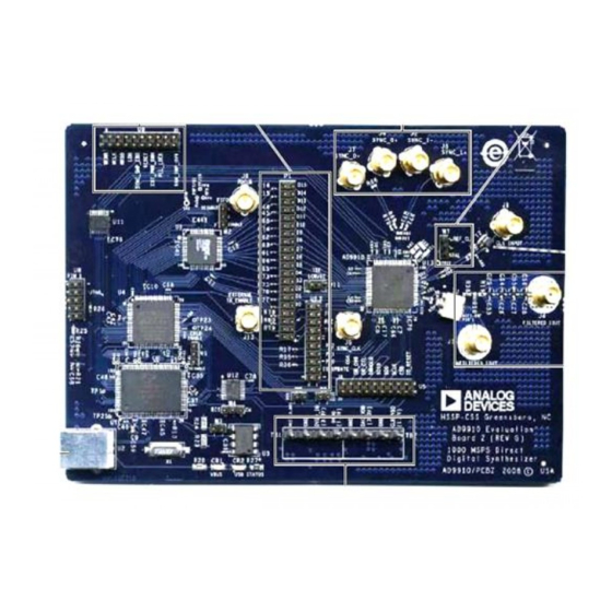
CONNECTIONS Figure 2. AD9910 PCB Evaluation Board Manual I/O Control Headers A 25 MHz crystal is provided on the underside of the AD9910 evaluation board. These pins provide the communication interface for the AD9910 when the part is under the command of an external Ref Clock Input controller (see Table 3 for correct jumper settings). -
Page 5: Evaluation Board Software
Once the software is successfully installed onto your PC, the Once the Found New Hardware Wizard window disappears, next step is to interface the AD9910 evaluation software to the AD9910 evaluation board via the USB Port (see Figure 2). the USB status LED (CR2 on the AD9910 evaluation board) - Page 6 Once the AD9910 evaluation software is loaded, a green splash board schematics for the AD9910. Check to make sure that the window appears. The status box within the splash window displays clock input source is connected and properly configured.
-
Page 7: Control Window
The maximum reference clock frequency of its specified range may result in undesired operation, including of the AD9910 is 1 GHz. The default setting is 100 MHz. A red nonfunctionality. See the AD9910 data sheet for more informa- outline indicates that the value entered is out of range. -
Page 8: Changes To Power Down Digital, Dac, Clock Input, And Aux Dac Section
Loading Data active, but does not allow the part to output data. This mode The LOAD button is used to send data to the AD9910. All uses significantly more power than the Full Power Down LOAD buttons found in the evaluation software have the same mode. -
Page 9: Profiles Window
Output Freq is used to set the frequency generated by the in decimal, hexadecimal, or binary format in the Tuning Word DDS. The AD9910 generates a sine/cosine wave at this output Values area. This window also allows you to enter in a tuning frequency. - Page 10 UG-207 Evaluation Board User Guide The Edit Phase Offset dialog box (see Figure 8) appears by double-clicking the Phase Offset text box in the Profiles window. The Edit Phase Offset window allows you to set individual bits in the phase offset word register. These bits can be typed in decimal, hexadecimal, or binary format in the Register Values area.
-
Page 11: View Windows
Evaluation Board User Guide UG-207 VIEW WINDOWS To access additional windows, select View from the AD9910 Evaluation Software drop-down menu bar. Figure 10. Windows Accessed from View Menu Rev. A | Page 11 of 16... -
Page 12: Osk And Digital Ramp Control
Digital Ramp Generator selected. It is important that the value in the Sweep 0 register To use the digital ramp generator (DRG) function of the AD9910, is always less than the value in the Sweep 1 register. select the Enable Digital Ramp Generator check box. Under... -
Page 13: Multichip Sync Control
The Multi-Chip Sync window allows you to set up the sync function. This allows you to sync multiple chips to one master To use the OSK function of the AD9910, select the Enable AD9910. Refer to the AD9910 data sheet for a full description Output Shift Keying check box. -
Page 14: Ram Operation
RAM OPERATION Figure 13. Profiles Window When Using the RAM Use of RAM on the AD9910 should not be attempted without RAM playback destination. Refer to the AD9910 data sheet for using the AD9910 data sheet as a reference. The AD9910 data further details on the RAM playback destination bits. -
Page 15: Debug
The RAM I/O Window allows you to easily interface RAM data and P1 control the profile register pins. See the AD9910 data into the AD9910. Use the RAM Data File box to locate the sheet for the logic to control the profiles via the external pins. -
Page 16: Change To Dut I/O Section
By using the evaluation board discussed herein (together with any tools, components documentation or support materials, the “Evaluation Board”), you are agreeing to be bound by the terms and conditions set forth below (“Agreement”) unless you have purchased the Evaluation Board, in which case the Analog Devices Standard Terms and Conditions of Sale shall govern. Do not use the Evaluation Board until you have read and agreed to the Agreement. -
Page 17: Deleted Ordering Information Section
Mouser Electronics Authorized Distributor Click to View Pricing, Inventory, Delivery & Lifecycle Information: Analog Devices Inc. AD9910/PCBZ...
Need help?
Do you have a question about the AD9910 and is the answer not in the manual?
Questions and answers