Table of Contents
Advertisement
Quick Links
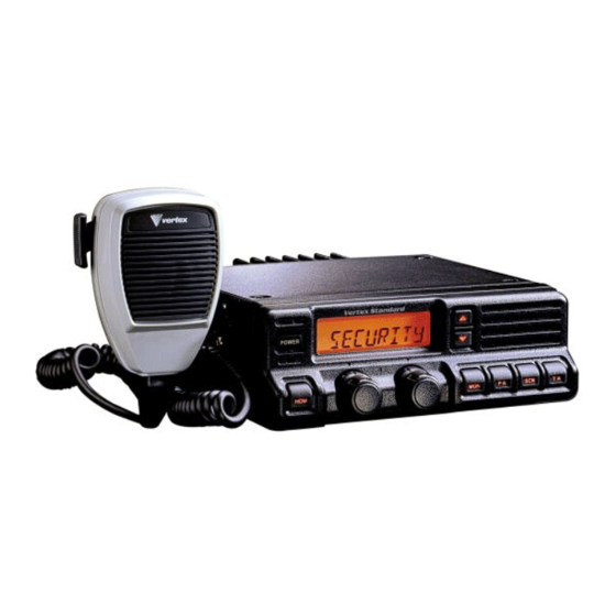
VHF Low-band FM Transceiver
VX-4000L
Service Manual
©2004 VERTEX STANDARD CO., LTD.
This manual provides technical information necessary for servicing the VX-4000L VHF Low-band FM Transceiver.
Servicing this equipment requires expertise in handling surface-mount chip components. Attempts by non-qualified
persons to service this equipment may result in permanent damage not covered by the warranty, and may be illegal in
some countries.
Two PCB layout diagrams are provided for each double-sided circuit board in the Transceiver. Each side of is referred
to by the type of the majority of components installed on that side ("leaded" or "chip-only"). In most cases one side has
only chip components, and the other has either a mixture of both chip and leaded components (trimmers, coils, electrolyt-
ic capacitors, ICs, etc.), or leaded components only.
While we believe the technical information in this manual to be correct, VERTEX STANDARD assumes no liability
for damage that may occur as a result of typographical or other errors that may be present. Your cooperation in pointing
out any inconsistencies in the technical information would be appreciated.
Operating Manual Reprint ......................... 1-1
Cloning .................................................................. 2-1
Specifications ................................................ 2-2
Block Diagram .............................................. 3-2
Interconnection Diagram............................ 3-4
Circuit Description ..................................... 4-1
Alignment...................................................... 5-1
EC005L90A
POWER
VERTEX STANDARD CO., LTD.
4-8-8 Nakameguro, Meguro-Ku, Tokyo 153-8644, Japan
VERTEX STANDARD
US Headquarters
10900 Walker Street, Cypress, CA 90630, U.S.A.
YAESU EUROPE B.V.
P.O. Box 75525, 1118 ZN Schiphol, The Netherlands
YAESU UK LTD.
Unit 12, Sun Valley Business Park, Winnall Close
Winchester, Hampshire, SO23 0LB, U.K.
VERTEX STANDARD HK LTD.
Unit 5, 20/F., Seaview Centre, 139-141 Hoi Bun Road,
Kwun Tong, Kowloon, Hong Kong
Board Unit
(Schematics, Layouts & Parts)
MAIN Unit ........................................................... 6A-1
DISPLAY Unit ...................................................... 6B-1
KEY Unit ............................................................... 6C-1
VR Unit ................................................................. 6D-1
MIC CONN Unit ................................................. 6D-2
Optional Board Unit
(Schematics, Layouts & Parts)
F2D-8 2-Tone Decode Unit ................................ 7A-1
F5D-14 5-Tone Unit ............................................. 7B-1
FVP-25 Encryption / DTMF Pager Unit ............ 7C-1
VTP-50 VX-Trunk Unit ...................................... 7D-1
1
Advertisement
Table of Contents

Related Manuals for Vertex Standard VX-4000L


Summary of Contents for Vertex Standard VX-4000L
-
Page 1: Table Of Contents
ICs, etc.), or leaded components only. While we believe the technical information in this manual to be correct, VERTEX STANDARD assumes no liability for damage that may occur as a result of typographical or other errors that may be present. Your cooperation in pointing out any inconsistencies in the technical information would be appreciated. -
Page 2: Operating Manual Reprint
Additional indicators on the display show prior- grammed by your VERTEX STANDARD dealer. ity channel assignments and scan include / ex- clude selection. ˆ... - Page 3 Operating Manual Reprint & C ONTROLS ONNECTORS Side Panel Microphone Jack (It is on both sides.) Connect the microphone plug to this jack. Microphone Jack REAR (Heatsink) • ‚ ƒ „ À Â Antenna Socket 13.8-V DC Cable Pigtail w/Connector The 50-ohm coaxial feedline to the antenna must The supplied DC power cable must be connected be connected here, using a type-M (PL-259) plug.
- Page 4 Operating Manual Reprint ASIC PERATION OF THE RANSCEIVER Important! - Before turning on the radio the first time, Transmitting confirm that the power connections have been made cor- To transmit, wait until the “BUSY” indicator is rectly and that a proper antenna is connected to the an- off (the channel is not in use), and press the PTT tenna jack.
- Page 5 For further details, contact your VERTEX STAN- by your VERTEX STANDARD dealer, to meet DARD dealer. For future reference, check the box your communications/network requirements. next to each function that has been assigned to...
- Page 6 After pressing the button, “TA” is displayed on the Watch”. LCD. m Operation will revert to the channel to which Noise Blanker (for VX-4000L) the CHANNEL selector knob is set. Because local noise can be particularly trouble- some in the VHF Low-Band frequency spectrum,...
- Page 7 Operating Manual Reprint DVANCED PERATION Alpha Numeric GRP UP/DWN Press the assigned PF button of the “Alpha Nu- Press the assigned PF button of the “GRP UP” or meric” to switch the display between the Group/ “GRP DWN” to select a different group of chan- Channel number, and the Group/Channel name nels.
- Page 8 Operating Manual Reprint DVANCED PERATION SQL (Squelch Level) You can manually adjust the squelch level using this function: 1. Press the assigned PF button of the “SQL”. A tone sounds and SQL appears on the display with the current squelch level. 2.
- Page 9 Operating Manual Reprint PTIONAL CCESSORIES MH-25 Microphone MH-53 Heavy Duty Microphone MH-53 Heavy Duty Microphone w/Noise Canceler MH-53 Heavy Duty DTMF Microphone w/Noise Canceler CE35 Programming Software CT-70 Radio Programming Cable (Requires VPL-1) CT-71 Radio to PC Programming Cable CT-72 Radio to Radio Programming Cable CT-81 Cable for RMK-4000 (6 m)
- Page 10 DSUB 25-P CCESSORY ONNECTOR DSUB 25-Pin Numbering None Pin 1: RSSI [Analog Output] This feature is the same as pressing A DC voltage proportional to the strength of the and holding in the Monitor key. signal currently being received (Receiver Signal LCD illumination dimmer “on.”...
- Page 11 Similarly, if you assign “CH SW0,” “CH SW1,” Pin 7: E [GND] and “CH SW2” to the Universal Input Port, you Ground for all logic levels and power supply re- can recall Channels 1~7 as shown below: turn. Channel CH SW0 CH SW1 CH SW2 Pin 8: AO2...
- Page 12 Pin 15: IGN Pin 19: NC [Ignition Sense feature] [No Connection] The VX-4000 may automatically be switched to Pins 20, 21, & 22: AO1, AO3 & AO4 the STAND-BY mode when the vehicle's igni-tion [Universal Output Port] key is turned on. LOGIC level (+5V / 0V) output.
- Page 13 Note: VX-4000 VHF Low-band Service Manual 1-12...
-
Page 14: Cloning
Cloning The VX-4000 includes a convenient “Clone” feature, Now, on the source transceiver, press and hold which allows the programming data from one trans- Button while turning the transceiver ceiver to be transferred to another VX-4000. Here is on.Data will now be transferred to the Destina- the procedure for Cloning one radio’s data to an- tion transceiver from the source transceiver. -
Page 15: Specifications
Specifications ENERAL Number of Channels: 250 channels Frequency Range: 29.7 - 37.0 MHz (A), 37.0 - 50 MHz (B) Channel Spacing: 5 / 10 / 12.5 / 15 / 20 / 25 / 50 kHz Power Supply Voltage: 13.8 VDC Current Consumption: Standby: 400 mA... -
Page 16: Exploded View & Miscellaneous Parts
Exploded View & Miscellaneous Parts À Screw List REF. VXSTD P/N Description Qty. RA0254900 CASE U20306007 BINDING HEAD SCREW M3x6B À U20306002 BINDING HEAD SCREW M3x6NI À U24308002 TAPTITE SCREW M3x8NI U23206001 TAPTITE SCREW M2.6x6 RA0262700 PACKING SHEET U20305007 BINDING HEAD SCREW M3x5B À... -
Page 17: Block Diagram
Block Diagram VX-4000 VHF Low-band Service Manual... - Page 18 Block Diagram VX-4000 VHF Low-band Service Manual...
-
Page 19: Interconnection Diagram
Interconnection Diagram VX-4000 VHF Low-band Service Manual... -
Page 20: Circuit Description
Circuit Description Reception and transmission are switched by “RX” 450 kHz by the 2nd mixer and stripped of unwant- and “TX” lines from the microprocessor unit (MPU). ed components by ceramic filter CF1002. After pass- ing through a limiter amplifier, the signal is demod- Signal Path Overview ulated by the FM detector. - Page 21 Circuit Description Transmitter DCS Demodulator Voice audio from the microphone is delivered via DCS signals are demodulated on the MAIN- the Mic (Jack) Unit to the MAIN Unit, after passing UNIT, and are applied to low-pass filter Q2110 through amplifier Q3039/Q2108 (NJM2902V), a pre- (NJM2902V), as well as the limiter comparator emphasis network, a limiter (IDC: instantaneous Q2110.
-
Page 22: Alignment
A dummy load and inline wattmeter must be con- Also, VERTEX STANDARD must reserve the right nected to the main antenna jack in all procedures to change circuits and alignment procedures in the... - Page 23 Alignment Before beginning, connect the transceiver and PC PLL & Transmitter using the CT-71 programming cable, and download Set up the test equipment as shown for transmit- the EEPROM data from the transceiver to the com- ter alignment. puter. Maintain the supply voltage at 13.8 V DC for all Store this data in a disk file so that it can be saved steps.
- Page 24 Alignment Transmitter Output Power Transmitter Deviation The following transmitter parameters can be ad- The following modulation parameters can be ad- justed from the computer by utilizing the Alignment justed from the computer by utilizing the Alignment Software. Refer to the onboard help of the Align- Software.
- Page 25 Alignment CTCSS Modulation Level Receiver r Stay on the band center frequency channel, with The sensitivity parameters can be adjusted from 151.4 Hz CTCSS encode, and reduce the AF gen- the computer by utilizing the Alignment Software. erator injection to zero. Refer to the onboard help of the Alignment Software r Key the transmitter and adjust (by control com- Manual for details.
- Page 26 MAIN Unit (Lot 1 ~) Circuit Diagram (2.23V) 1.55V (0V) 0.75V (5.55V) 13.8V (1.01V) (13.8V) (5.55V) (0.96V) 13.75V 8.79V (5.17V) (4.71V) 1.98V (5.28V) 1.25V (5.21V) (0.0V) 6.04V 0.0V 2.24V (5.66V) 0.22V (4.34V) (0.0V) 8.82V (0.00V) (8.86V) 7.81V 1.90V (7.80V) (8.17V) (2.90V) 1.77V (1.48V)
- Page 27 MAIN Unit (Lot 1 ~) 1.28V 4.88V 1.1V (1.1V) (12.47V) (4.88V) 1.86V 0.01V (1.1V) 8.64V (0.78V) (1.19V) 0.14V (8.65V) (2.09V) 0.0V (3.6V) (12.99V) 1.1V (1.1V) 0.0V 4.87V (2.09V) (4.87V) (0.31V) 4.86V 0.01V 0.0V (0.77V) (4.86V) (0.81V) 1.31V (1.1V) 0.0V (4.19V) 1.76V (1.18V) 0.0V...
- Page 28 MAIN Unit (Lot 1 ~) Parts Layout MB90F583B 2SC3240-21 (Q2019) (Q1013) NJM2902V SA7025DK (Q1007) (Q1024) TA31136FN BU4066BF (Q1026) (Q2007) CXA1846N HN58X2432TI (Q2014) (Q2028) TC4W53FU TDA7240AV 2SK3074 (WA) (Q2117) (Q2029) (Q1020) 2SK2035 (KP) 2SA1602A (MF) 3SK131 (V12) (Q1034) (Q1035) (Q1501, 1502) 3SK240 (UN) (Q1012, 1025) 2SC4154E (LE)
- Page 29 MAIN Unit (Lot 1 ~) NJM2902V 2SB1201STP BU4053BCF 2SJ327Z MX165CDW (Q2001, 2003, 2108 (Q1003) 2SC3133-21 (Q2016) (Q2020) (Q2013) 2110) (Q2131) IMH6 (H6) TA75S01F (SA) IMD3 (D3) (Q1009) (Q1038) (Q1503, 2115) IMZ1 (Z1) IMX1 (X1) DTB123EK (F12) (Q2002) (Q2009) (Q1005, 2015, 2111) RT1N241M (N2) 2SC4154E (LE) 2SC5415E (EA)
- Page 30 MAIN Unit (Lot 8 ~) Circuit Diagram 6A-5 VX-4000 VHF Low-band Service Manual...
- Page 31 MAIN Unit (Lot 8 ~) 6A-6 VX-4000 VHF Low-band Service Manual...
- Page 32 MAIN Unit (Lot 8 ~) Parts Layout MB90F583B 2SC3240-21 (Q2019) (Q1013) NJM2902V SA7025DK (Q1007) (Q1024) TA31136FN BU4066BF (Q1026) (Q2007) CXA1846N HN58X2432TI (Q2014) (Q2028) TC4W53FU TDA7240AV 2SK3074 (WA) (Q2117) (Q2029) (Q1020) 2SK2035 (KP) 2SA1602A (MF) 3SK131 (V12) (Q1034) (Q1035) (Q1501, 1502) 3SK240 (UN) (Q1012, 1025) 2SC4154E (LE)
- Page 33 MAIN Unit (Lot 8 ~) NJM2902V 2SB1201STP BU4053BCF 2SJ327Z MX165CDW (Q2001, 2003, 2108 (Q1003) 2SC3133-21 (Q2016) (Q2020) (Q2013) 2110) (Q2131) IMH6 (H6) TA75S01F (SA) IMD3 (D3) (Q1009) (Q1038) (Q1503, 2115) IMZ1 (Z1) IMX1 (X1) DTB123EK (F12) (Q2002) (Q2009) (Q1005, 2015, 2111) RT1N241M (N2) 2SC4154E (LE) 2SC5415E (EA)
-
Page 34: Main Unit
MAIN Unit Parts List REF. DESCRIPTION VALUE TOL. MFR’S DESIG VXSTD P/N VERS. LOT. SIDE. LAY ADR. *** MAIN UNIT *** PCB with Components CS1760001 Printed Circuit Board FR005770C Printed Circuit Board FR005770D C 1001 CHIP CAP. 68pF GRM39CH680J50PT K22174231 C 1001 CHIP CAP. - Page 35 MAIN Unit REF. DESCRIPTION VALUE TOL. MFR’S DESIG VXSTD P/N VERS. LOT. SIDE. LAY ADR. C 1056 CHIP CAP. 0.5pF GRM39CK0R5C50PT K22174201 C 1057 CHIP CAP. 0.001uF GRM39CH102J25PT K22144204 C 1058 CHIP CAP. 0.01uF GRM39B103M50PT K22174823 C 1059 CHIP CAP. 0.01uF GRM39B103J50PT K22174824...
- Page 36 MAIN Unit REF. DESCRIPTION VALUE TOL. MFR’S DESIG VXSTD P/N VERS. LOT. SIDE. LAY ADR. C 1114 CHIP CAP. 68pF GRM39CH680J50PT K22174231 C 1115 CHIP TA.CAP. 4.7uF TEMSVA1C475M-8R K78120031 C 1117 CHIP CAP. 22pF GRM39CH220J50PT K22174219 C 1117 CHIP CAP. 22pF GRM39CH220J50PT K22174219 VERSION A 4-...
- Page 37 MAIN Unit REF. DESCRIPTION VALUE TOL. MFR’S DESIG VXSTD P/N VERS. LOT. SIDE. LAY ADR. C 1166 CHIP CAP. 0.01uF GRM39B103M50PT K22174823 C 1169 CHIP CAP. 12pF GRM39CH120J50PT K22174213 C 1170 CHIP CAP. 0.1uF GRM39B104K16PT K22124805 C 1171 CHIP CAP. 150pF GRM39CH151J50PT K22174239...
- Page 38 MAIN Unit REF. DESCRIPTION VALUE TOL. MFR’S DESIG VXSTD P/N VERS. LOT. SIDE. LAY ADR. C 1255 CHIP CAP. 68pF GRM39CH680J50PT K22174231 C 1256 CHIP CAP. 0.01uF GRM39B103J50PT K22174824 C 1257 CHIP CAP. 0.001uF GRM39B102K50PT K22174821 C 1258 CHIP TA.CAP. 10uF TEMSVA1A106M-8R K78100028...
- Page 39 MAIN Unit REF. DESCRIPTION VALUE TOL. MFR’S DESIG VXSTD P/N VERS. LOT. SIDE. LAY ADR. C 1334 CHIP CAP. 0.01uF GRM39B103J50PT K22174824 C 1335 CHIP CAP. GRM42-2B105K50PT K22175801 VERSION B 6- C 1336 CHIP CAP. GRM42-2B105K50PT K22175801 VERSION B 6- C 1341 CHIP CAP.
- Page 40 MAIN Unit REF. DESCRIPTION VALUE TOL. MFR’S DESIG VXSTD P/N VERS. LOT. SIDE. LAY ADR. C 2007 CHIP CAP. 100pF GRM39CH101J50PT K22174235 C 2008 CHIP CAP. 100pF GRM39CH101J50PT K22174235 C 2009 CHIP CAP. 100pF GRM39CH101J50PT K22174235 C 2010 CHIP CAP. 100pF GRM39CH101J50PT K22174235...
- Page 41 MAIN Unit REF. DESCRIPTION VALUE TOL. MFR’S DESIG VXSTD P/N VERS. LOT. SIDE. LAY ADR. C 2073 CHIP CAP. 0.01uF GRM39B103M50PT K22174823 C 2074 CHIP CAP. 470pF GRM39CH471J50PT K22174249 C 2075 CHIP TA.CAP. TESVA1C105M1-8R K78120009 C 2076 CHIP CAP. 470pF GRM39CH471J50PT K22174249 C 2078 CHIP CAP.
- Page 42 MAIN Unit REF. DESCRIPTION VALUE TOL. MFR’S DESIG VXSTD P/N VERS. LOT. SIDE. LAY ADR. C 2138 CHIP TA.CAP. 4.7uF TEMSVA1C475M-8R K78120031 C 2139 CHIP CAP. 0.1uF GRM39B104K16PT K22124805 C 2140 CHIP CAP. 0.1uF GRM39B104K16PT K22124805 C 2141 CHIP TA.CAP. 4.7uF TEMSVA1C475M-8R K78120031...
- Page 43 MAIN Unit REF. DESCRIPTION VALUE TOL. MFR’S DESIG VXSTD P/N VERS. LOT. SIDE. LAY ADR. D 1018 DIODE HVU306A5TRF G2070132 D 1019 DIODE HVU359TRF G2070452 D 1019 DIODE HVC359 TRF G2070708 D 1020 DIODE HVU356TRF G2070306 D 1022 DIODE HVU356TRF G2070306 D 1024 DIODE 1SS321 TE85R...
- Page 44 MAIN Unit REF. DESCRIPTION VALUE TOL. MFR’S DESIG VXSTD P/N VERS. LOT. SIDE. LAY ADR. J 2001 CONNECTOR JBY-25S-1A3F P1090815 J 2004 CONNECTOR BM03B-SRSS-TBT P0091301 J 2005 CONNECTOR AXN426C530P P0091296 L 1001 COIL E2 0.25-1.85-8.5T-L L0022576 L 1001 COIL E2 0.25-1.85-8.5T-L L0022576 VERSION A 4- L 1001 COIL...
- Page 45 MAIN Unit REF. DESCRIPTION VALUE TOL. MFR’S DESIG VXSTD P/N VERS. LOT. SIDE. LAY ADR. L 1038 CHIP COIL 0.22uH C2520C-R22J L1690548 L 1038 CHIP COIL 0.22uH C2520C-R22J L1690548 VERSION A 4- L 1038 CHIP COIL 0.15uH C2520C-R15J L1690546 VERSION B 4- L 1038 CHIP COIL 0.1uH C2520C-R10J...
- Page 46 Q 2110 IC NJM2902V-TE1 G1091679 Q 2111 TRANSISTOR DTB123EK T146 G3070022 Q 2112 TRANSISTOR IMD3 T108 G3070053 Q 2114 TRANSISTOR RT1N241M-T11-1 G3070249 Q 2115 TRANSISTOR IMD3 T108 G3070053 Requires Firmware, CE35 and FIF-8. Please contact VERTEX STANDARD. VX-4000 VHF Low-band Service Manual...
- Page 47 MAIN Unit REF. DESCRIPTION VALUE TOL. MFR’S DESIG VXSTD P/N VERS. LOT. SIDE. LAY ADR. Q 2116 TRANSISTOR RT1N241M-T11-1 G3070249 Q 2117 IC TC4W53FU TE12L G1091675 Q 2118 TRANSISTOR RT1N241M-T11-1 G3070249 Q 2119 TRANSISTOR RT1N241M-T11-1 G3070249 Q 2120 TRANSISTOR RT1N241M-T11-1 G3070249 Q 2121 TRANSISTOR RT1N241M-T11-1...
- Page 48 MAIN Unit REF. DESCRIPTION VALUE TOL. MFR’S DESIG VXSTD P/N VERS. LOT. SIDE. LAY ADR. R 1047 CHIP RES. 1/16W 5% RMC1/16 223JATP J24185223 R 1048 CHIP RES. 4.7k 1/16W 5% RMC1/16 472JATP J24185472 R 1049 CHIP RES. 1/16W 5% RMC1/16 103JATP J24185103 R 1051 CHIP RES.
- Page 49 MAIN Unit REF. DESCRIPTION VALUE TOL. MFR’S DESIG VXSTD P/N VERS. LOT. SIDE. LAY ADR. R 1115 CHIP RES. 220k 1/16W 5% RMC1/16 224JATP J24185224 R 1117 CHIP RES. 1/16W 5% RMC1/16 102JATP J24185102 R 1118 CHIP RES. 1/16W 5% RMC1/16 473JATP J24185473 R 1119 CHIP RES.
- Page 50 MAIN Unit REF. DESCRIPTION VALUE TOL. MFR’S DESIG VXSTD P/N VERS. LOT. SIDE. LAY ADR. R 1318 METAL FILM RES. ERG-3SJ101P 100 J22359023 VERSION B 6- R 1318 METAL FILM RES. ERG-3SJ220P 22 J22359025 VERSION B 8- R 1319 CHIP RES. RMC1 101JTE J24305101 VERSION B 6-7 R 1320 CHIP RES.
- Page 51 MAIN Unit REF. DESCRIPTION VALUE TOL. MFR’S DESIG VXSTD P/N VERS. LOT. SIDE. LAY ADR. R 2036 CHIP RES. 1/16W 5% RMC1/16 223JATP J24185223 R 2037 CHIP RES. 120k 1/16W 5% RMC1/16 124JATP J24185124 R 2038 CHIP RES. 4.7k 1/16W 5% RMC1/16 472JATP J24185472 R 2039 CHIP RES.
- Page 52 MAIN Unit REF. DESCRIPTION VALUE TOL. MFR’S DESIG VXSTD P/N VERS. LOT. SIDE. LAY ADR. R 2100 CHIP RES. 180k 1/16W 5% RMC1/16 184JATP J24185184 R 2101 CHIP RES. 180k 1/16W 5% RMC1/16 184JATP J24185184 R 2102 CHIP RES. 1/16W 5% RMC1/16 153JATP J24185153 R 2103 CHIP RES.
- Page 53 MAIN Unit REF. DESCRIPTION VALUE TOL. MFR’S DESIG VXSTD P/N VERS. LOT. SIDE. LAY ADR. R 2166 CHIP RES. 1/16W 5% RMC1/16 000JATP J24185000 R 2168 CHIP RES. 1/16W 5% RMC1/16 103JATP J24185103 R 2169 CHIP RES. 1/16W 5% RMC1/16 103JATP J24185103 R 2175 CHIP RES.
- Page 54 MAIN Unit REF. DESCRIPTION VALUE TOL. MFR’S DESIG VXSTD P/N VERS. LOT. SIDE. LAY ADR. R 2242 CHIP RES. 1/16W 5% RMC1/16 102JATP J24185102 R 2243 CHIP RES. 1/16W 5% RMC1/16 102JATP J24185102 R 2243 CHIP RES. 1/16W 5% RMC1/16 000JATP J24185000 R 2244 CHIP RES.
- Page 55 MAIN Unit Note: VX-4000 VHF Low-band Service Manual...
- Page 56 DISPLAY Unit Circuit Diagram (13.77V) (12.89V) (13.16V) (4.48V) (3.94V) (4.63V) (7.71V) (5.7V) (3.73V) (5.81V) (3.91V) (4.94V) (2.29V) 2.26V (3.27V) (2.39V) MON On:(2.92V) (1.65V) (3.84V) (4.95V) (4.92V) (0V) (2.16V) (2.18V) (2.18V) (4.82V) (12.32V) (4.96V) (4.97V) (2.18V) (4.97V) (3.92V) (0.02~4.83V) (4.95V) (13.07V) (4.62V) (4.26V) (0.77V)
- Page 57 DISPLAY Unit Note: 6B-2 VX-4000 VHF Low-band Service Manual...
- Page 58 DISPLAY Unit Parts Layout Side A S-93C46AMFN-TB 2SB1132Q (BA) RT1N241M (N2) NJM78L05UA (8C) MC2848 (A6) DAP202U (P) MC2850 (A7) (Q3012) (Q3031) (Q3003) (Q3021) (D3008) (D3006) (D3018, 3019) 6B-3 VX-4000 VHF Low-band Service Manual...
- Page 59 DISPLAY Unit Parts Layout Side B NJM2902V (Q3039) S-80735SN (DZ) IMD3 (D3) IMZ1 (Z1) 2SC4154E (LE) RT1N241M (N2) 1SS226 (C3) HD64F3642AH (Q3016) (Q3013) (Q3004, 3011, 3040) (Q3019) (Q3005, 3008, 3009 (D3005) (Q3014) IMX1 (X1) 3020, 3022, 3024 (Q3010, 3038) 3025, 3026, 3027) 2SB1132Q (BA) (Q3028, 3029) TC4S66F (C9)
-
Page 60: Display Unit
DISPLAY Unit Parts List REF. DESCRIPTION VALUE TOL. MFR’S DESIG VXSTD P/N VERS. LOT. SIDE. LAY ADR. *** DISPLAY UNIT *** PCB with Components CB1294001 Printed Circuit Board FR004690D C 3001 CHIP CAP. 0.1uF GRM39B104K16PT K22124805 C 3002 CHIP CAP. 0.1uF GRM39B104K16PT K22124805... - Page 61 IMH6A T108 G3070066 Q 3038 TRANSISTOR IMX1 T110 G3070024 Q 3039 IC NJM2902V-TE1 G1091679 Q 3040 TRANSISTOR IMZ1 T108 G3070025 Q 3043 IC TC4S66F TE85R G1090893 Requires Firmware, CE35 and FIF-8. Please contact VERTEX STANDARD. 6B-6 VX-4000 VHF Low-band Service Manual...
- Page 62 DISPLAY Unit REF. DESCRIPTION VALUE TOL. MFR’S DESIG VXSTD P/N VERS. LOT. SIDE. LAY ADR. R 3002 CHIP RES. 1/16W 5% RMC1/16 473JATP J24185473 R 3004 CHIP RES. 2.2k 1/16W 5% RMC1/16 222JATP J24185222 R 3006 CHIP RES. 1/16W 5% RMC1/16 563JATP J24185563 R 3007 CHIP RES.
- Page 63 DISPLAY Unit REF. DESCRIPTION VALUE TOL. MFR’S DESIG VXSTD P/N VERS. LOT. SIDE. LAY ADR. R 3075 CHIP RES. 1/16W 5% RMC1/16 103JATP J24185103 R 3076 CHIP RES. 1/16W 5% RMC1/16 473JATP J24185473 R 3077 CHIP RES. 1/16W 5% RMC1/16 473JATP J24185473 R 3078 CHIP RES.
- Page 64 DISPLAY Unit REF. DESCRIPTION VALUE TOL. MFR’S DESIG VXSTD P/N VERS. LOT. SIDE. LAY ADR. R 3152 CHIP RES. 4.7k 1/16W 5% RMC1/16 472JATP J24185472 R 3153 CHIP RES. 4.7k 1/16W 5% RMC1/16 472JATP J24185472 R 3154 CHIP RES. 4.7k 1/16W 5% RMC1/16 472JATP J24185472...
- Page 65 DISPLAY Unit Note: 6B-10 VX-4000 VHF Low-band Service Manual...
- Page 66 KEY Unit Circuit Diagram 1.96V 3.9V 5.8V 1.92V 3.82V 4.62V 7.71V 4.95V 4.61V 3.18V 3.87V 4.19V 4.34V 4.46V 4.53V 2SA1602A (MF) (Q3401) Parts Layout Side A Side B 6C-1 VX-4000 VHF Low-band Service Manual...
- Page 67 KEY Unit Note: 6C-2 VX-4000 VHF Low-band Service Manual...
-
Page 68: Key Unit
KEY Unit Parts List REF. DESCRIPTION VALUE TOL. MFR’S DESIG VXSTD P/N VERS. LOT. SIDE. LAY ADR. *** KEY UNIT *** PCB with Components CB1703001 Printed Circuit Board FR006070D C 3402 CHIP CAP. 0.001uF GRM39B102K50PT K22174821 D 3401 LED TLOU1008(T4) G2070796 D 3402 LED TLOU1008(T4) - Page 69 KEY Unit Note: VX-4000 VHF Low-band Service Manual 6C-4...
-
Page 70: Vr Unit
VR Unit Circuit Diagram Parts Layout R3606 C3603 J3601 R3602 S3601 R3603 R3607 R3605 C3604 VR3601 C3606 Side A Side B Parts List REF. DESCRIPTION VALUE TOL. MFR’S DESIG VXSTD P/N VERS. LOT. SIDE. LAY ADR. *** VR UNIT *** PCB with Components CB1704001 Printed Circuit Board... -
Page 71: Mic Conn Unit
MIC CONN Unit Circuit Diagram Parts Layout Side A Side B Parts List REF. DESCRIPTION VALUE TOL. MFR’S DESIG VXSTD P/N VERS. LOT. SIDE. LAY ADR. *** MIC CONN UNIT *** PCB with Components CB1705001 Printed Circuit Board FR006090C C 3906 CHIP CAP. 0.01uF GRM39B103M50PT K22174823... -
Page 72: F2D-8 2-Tone Decode Unit
F2D-8 2-Tone Decode Unit Circuit Diagram Parts Layout Side A Side B TC7S04FU (E5) TA75S01F (SA) DTC124TU (05) HD64F3334YTF16 (Q1003) (Q1004) (Q1005) (Q1001) VX-4000 VHF Low-band Service Manual 7A-1... - Page 73 F2D-8 2-Tone Decode Unit Parts List REF. DESCRIPTION VALUE TOL. MFR’S DESIG VXSTD P/N VERS. LOT. SIDE LAY ADR *** F2D-8 *** Printed Circuit Board FR002530C C 1001 CHIP TA.CAP. 4.7uF 6.3V TEMSVA0J475M-8R K78080017 C 1002 CHIP CAP. 0.001uF GRM39B102K50PT K22174821 C 1003 CHIP CAP.
-
Page 74: F5D-14 5-Tone Unit
F5D-14 5-Tone Unit Circuit Diagram Parts Layout Side A Side B TK71650SC (L50) DTC114TE (04) PIC17LC44-08/PQ 2SC4617 (BR) MD09 BR93LC66FV (Q1001) (Q1002) (Q1003) (Q1004) (Q1005) (Q1006) VX-4000 VHF Low-band Service Manual 7B-1... - Page 75 F5D-14 5-Tone Unit Parts List REF. DESCRIPTION VALUE TOL. MFR’S DESIG VXSTD P/N VERS. LOT. SIDE LAY ADR *** F5D-14 *** Printed Circuit Board FR006510B Printed Circuit Board FR006510D C 1001 CHIP CAP. 0.1uF GRM36B104K10PT K22108802 C 1002 CHIP CAP. 0.0018uF GRM36B182K50PT K22178812...
-
Page 76: Fvp-25 Encryption / Dtmf Pager Unit
FVP-25 Encryption / DTMF Pager Unit Circuit Diagram Parts Layout Side A Side B M64026FP LC73881 DTC144EU (26) (Q1001) (Q1002) (Q1003) VX-4000 VHF Low-band Service Manual 7C-1... - Page 77 FVP-25 Encryption / DTMF Pager Unit Parts List REF. DESCRIPTION VALUE TOL. MFR’S DESIG VXSTD P/N VERS. LOT. SIDE LAY ADR *** FVP-25 *** Printed Circuit Board FR005010F C 1001 CHIP CAP. 0.1uF GRM39B104K16PT K22124805 C 1002 CHIP CAP. 0.01uF GRM39B103M25PT K22144802 C 1003 CHIP CAP.
- Page 78 VTP-50 VX-Trunk Unit Circuit Diagram Parts Layout Side B Side A BR93LC56FV NJM2904V MC68HSC705C8A502 TA75S01F (SA) (Q1001) (Q1003) (Q1004) (Q1002) VX-4000 VHF Low-band Service Manual 7D-1...
- Page 79 VTP-50 VX-Trunk Unit Parts List REF. DESCRIPTION VALUE TOL. MFR’S DESIG VXSTD P/N VERS. LOT. SIDE LAY ADR *** VTP-50 *** Printed Circuit Board FR002540C C 1002 CHIP CAP. 0.001uF GRM39B102K50PT K22174821 C 1003 CHIP CAP. 0.01uF GRM39B103M25PT K22144802 C 1003 CHIP CAP. 0.01uF GRM39B103K25PT K22144803...
- Page 80 No portion of this manual may be © Copyright 2003 reproduced without the permission VERTEX STANDARD CO., LTD. of VERTEX STANDARD CO., LTD. All rights reserved VX-4000 VHF Low-band Service Manual 7D-4...
Need help?
Do you have a question about the VX-4000L and is the answer not in the manual?
Questions and answers