Table of Contents
Advertisement
Quick Links
Freescale Semiconductor
User Guide
P4080 Development System User's Guide
by
Networking and Multimedia Group
Freescale Semiconductor, Inc.
Austin, TX
1
Overview
The P4080 development system (DS) is a high-performance
computing, evaluation, and development platform
supporting the P4080 Power Architecture® processor. The
P4080 development system's official designation is
P4080DS, and may be ordered using this part number.
The P4080DS is designed to the ATX form-factor standard,
allowing it to be used in 2U rack-mount chassis, as well as in
a standard ATX chassis. The system is lead-free and
RoHS-compliant.
© 2011 Freescale Semiconductor, Inc. All rights reserved.
Document Number: P4080DSUG
Rev. 0, 07/2010
Contents
1. Overview . . . . . . . . . . . . . . . . . . . . . . . . . . . . . . . . . . . 1
2. Features Summary . . . . . . . . . . . . . . . . . . . . . . . . . . . 2
3. Block Diagram and Placement . . . . . . . . . . . . . . . . . . 4
4. Evaluation Support . . . . . . . . . . . . . . . . . . . . . . . . . . . 6
5. Architecture . . . . . . . . . . . . . . . . . . . . . . . . . . . . . . . . 8
6. Configuration . . . . . . . . . . . . . . . . . . . . . . . . . . . . . . 40
7. Programming Model . . . . . . . . . . . . . . . . . . . . . . . . . 45
8. Revision History . . . . . . . . . . . . . . . . . . . . . . . . . . . . 58
A. References . . . . . . . . . . . . . . . . . . . . . . . . . . . . . . . . 58
Advertisement
Table of Contents

Related Manuals for NXP Semiconductors P4080


Summary of Contents for NXP Semiconductors P4080
-
Page 1: Table Of Contents
2. Features Summary ......2 The P4080 development system (DS) is a high-performance 3. Block Diagram and Placement ....4 computing, evaluation, and development platform 4. -
Page 2: Features Summary
– Two serial ports at up to 115200 Kbps — Debug features – Both Legacy COP/JTAG and Aurora/Nexus debug support – EVT support — Package – 1295-pin, 1 mm pitch BGA – Socket and solder attach can be supported. P4080 Development System User’s Guide, Rev. 0 Freescale Semiconductor... - Page 3 Power supplies — Three dedicated programmable regulators supplying two cores and platform power pools — PMBus control — GVDD (DDR power) and VTT/VREF adjustable for DDR3 — 2.5-V power for Ethernet PHY P4080 Development System User’s Guide, Rev. 0 Freescale Semiconductor...
-
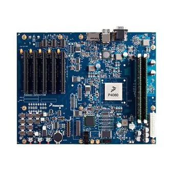
Page 4: Block Diagram And Placement
COP Legacy conn COP Legacy conn Run Control/Trace conn Run Control/Trace conn independent programmable regulators Clocks CPU 0:3 DUART RTC/BAT RTC/BAT Regulators P4080 CPU 4:7 Platform/Serdes FLASH/RCW FLASH/RCW (OCTAL CORE) System DDR3Regulator DDR3 2 Control /PM Logic FPGA Local Bus... - Page 5 Block Diagram and Placement This figure highlights more difficult-to-find connections that are commonly used. Notes: I2C HEADERS AURORA and LEGACY COP CONNECTORS ATX POWER CONNECTORS CPU FAN HEADER Figure 2. Expedition Top View P4080 Development System User’s Guide, Rev. 0 Freescale Semiconductor...
-
Page 6: Evaluation Support
Evaluation Support Evaluation Support The P4080DS is intended to evaluate as many features of the P4080 as are reasonable within a limited amount of board space and cost limitations. This table shows an evaluation of the P4080DS. Table 1. P4080DS Evaluation Summary... - Page 7 For many test situations, it is desirable to download a test vector program and run the results. The P4080DS can do this by using a PCI-based control card, such as the DataBlizzard, or a PCI Express-based control P4080 Development System User’s Guide, Rev. 0 Freescale Semiconductor...
-
Page 8: Architecture
Results can be extracted from system DDR, PCI Express graphics memory (used as a buffer), or other memory (SDMedia, Flash, PromJet). Architecture The P4080DS architecture is primarily determined by the P4080 processor, and by the need to provide “typical,” OS-dependent resources (disk, Ethernet, and so on). Processor This table lists the major pin groupings of the P4080. - Page 9 “Power” 5.1.1 The P4080 supports DDR2 and DDR3 devices; however, the P4080DS supports only DDR3 , using industry-standard JEDEC DDR3 2-rank and 4-rank DIMM modules. However, the system is shipped and supported by software to support UDIMM 2-rank modules for targeted vendors. The type and vendor may change as memory availability varies.
- Page 10 The DDR3 power supplies the following interface voltages: • VDD_IO up to 20 W (10 A at 1.5 V nominal) • VDDQ+VTT up to 2 A • MVREF up to 10 mA P4080 Development System User’s Guide, Rev. 0 Freescale Semiconductor...
- Page 11 Architecture 5.1.1.1 Compatible DDR-3 Modules The DDR interface of the P4080DS and the P4080 works with any JEDEC-compliant, 240-pin, DDR3 DIMM module. This table shows several DIMM modules that are believed to be compatible. Table 4. DDR-3 Modules Mfg. Part Number...
- Page 12 Cards Only TX/RX[0:3](p,n) Aurora Conn SD_TX/RX[8;9](p,n) TX/RX[1:0](p,n) REFCLK_SD1(p,n) 100 MHz Figure 5. SerDes Bank1 Configuration Note that a Mid-bus probe can be used with a logic analyzer to analyze bus activity. P4080 Development System User’s Guide, Rev. 0 Freescale Semiconductor...
- Page 13 Note that the Mid-bus probes are not on the development system, but are available on the SGMII and XAUI riser cards. The SD2 and SD3 clocking domains are separate clock generators. P4080 Development System User’s Guide, Rev. 0 Freescale Semiconductor...
- Page 14 5.1.3 Ethernet (EC) The P4080 supports up to two 10/100/1000baseT triple-speed Ethernet controllers (EC). The P4080DS uses one of these, which is channel EC2, and is connected to the on-board Vitesse VSC8244 PHY (the remaining ports are unused) using the RGMII protocol. Alternately, both ECs may be independently connected to a ULPI USB interface;...
- Page 15 Support for IEEE Std 1588 Protocol The P4080 includes support for the IEEE 1588 precision time protocol (PTP). This facility works in tandem with the Ethernet controller to time-stamp incoming packets. This figure shows an overview of the IEEE 1588 block.
- Page 16 Figure 9. Local Bus Overview The P4080 can redirect boot fetches to the eLBC, where it is routed to the device attached to LCS0. To support greater flexibility, the ngPIXIS can re-route the LCS0 pin to other devices, allowing the P4080DS to boot from the following devices: •...
- Page 17 Boot from NOR Flash region #7 1000 LCS1 LCS0 LCS[2,4:6] — Boot from PromJet, NOR Flash unbanked. 1001 LCS2 LCS1 LCS[0,4:6] — Boot from NAND Flash NOR Flash unbanked. 1010–1111 Not valid P4080 Development System User’s Guide, Rev. 0 Freescale Semiconductor...
- Page 18 7, the Flash behaves normally or is swapped around as virtual banks. Thus, the boot bank can be swapped around to support up to eight boot images with or without RCW. P4080 Development System User’s Guide, Rev. 0 Freescale Semiconductor...
- Page 19 5.1.6 eSDHC The P4080 has an enhanced secure digital host controller (eSHDC). The P4080DS connects the eSDHC to an SDMedia card slot and uses GPIO signals for sideband signals, such as write-protect-detect and card-detect. Both x4 and x8 cards are supported, the latter using the SPI_CS_B[0:3] signals, which can be reassigned as eSHDC_D[4:7].
-
Page 20: Spi Interface
5.1.7 SPI Interface The P4080 has a serial peripheral interface (SPI), which is used to communicate with various peripherals. The P4080DS connects a conventional 16-Mbyte serial EEPROM to one chip-select. The remaining three chip-selects are unused. This figure shows the overall connections of the SPI portion. -
Page 21: Usb Interface
USB Interface The P4080 has a USB 2.0 port that uses the UTMI+ protocol to connect to an external USB PHY, and may be configured for host or device modes. This figure shows the overall connections of the USB portion. - Page 22 5.1.11 GPIO Controller Port Several pins of the P4080 can be used for customer-specific applications. Some of these pins have alternate P4080-defined purposes to which they may also be used. All unused GPIO signals are connected to test points on the P4080DS board; for those that have additional functions, there are additional connections as noted.
- Page 23 FPGA can inject system-level resets along with the legacy COP or Aurora resets. Note that the Legacy COP HRST is mapped to the P4080 PORESET and the Legacy COP SRST is mapped to the P4080 HRESET. The P4080 HRESET is bi-directional open drain signal, but is not monitored by the ngPIXIS FPGA.
- Page 24 (DLL and DML) are typically done by reading the ngPIXIS PX_CLK register to determine the P4080 SYSCLK clock input (typically 133 MHz) frequency, but possibly any value. The baud rate divisors can then be calculated using the formula described in the P4080 QorIQ Integrated Communications Processor Family Reference Manual.
- Page 25 Write protectable. ngPIXIS I2C port Used for bus reset, monitoring, and master-only data collection. I2C Access Header For remote programming of boot sequencer startup code (if needed) or Zilker Lab PMBus programmer. P4080 Development System User’s Guide, Rev. 0 Freescale Semiconductor...
- Page 26 5.1.15 EM1 and EM2 Management Busses The P4080 has two types buses: one for SGMII and RGMII PHY management, and one for XAUI PHY management. Because one set of busses must span across multiple devices in the P4080DS system, multiplexers are used to route from the P4080 to each PHY. GPIOs are used to control the multiplexers.
- Page 27 CLK_OUT Test point w/adjacent ground. ASLEEP ngPIXIS 5.1.17 Clock This table summarizes the clocks for the P4080. Further details on the clock architecture are covered in Section 5.4, “Clocks.” Table 14. P4080 Clock Connections Pin Count Signal Names Connections SYSCLK...
- Page 28 Figure 17. Functional Block Diagram of P4080DS Thermal Management Scheme 5.1.19 Power The power requirements of the P4080 are estimated at this time, based on historical precedents and estimated power requirements. These figures show the power architecture for the P4080 as implemented on the P4080DS.
- Page 29 Architecture P4080 Figure 19. P4080DS Power Architecture for P4080 Part 2of 3 P4080 Figure 20. P4080DS Power Architecture for P4080 Part 3 of 3 P4080 Development System User’s Guide, Rev. 0 Freescale Semiconductor...
- Page 30 Architecture Note that this is the power for the P4080 only as implemented on the P4080DS; it does not include external devices, memory, and so on. Because these are estimates, and because alpha silicon tends to be “hot,” the VDD rail must have an excess capacity of approximately 20%.
- Page 31 Drives resets from the sequencer, from register-based software control, or from VELA REGISTERS A multi-ported register file containing status and configuration data LOCALBUS Interface between processor and REGFILE CONFIG Monitors and/or sets selected configuration signals P4080 Development System User’s Guide, Rev. 0 Freescale Semiconductor...
- Page 32 Offline configuration manager—a machine that initializes the ngPIXIS registers, including those used for P4080 initialization, from external I C EEPROMs. The OCM can talk to the user or another computer using the serial port while the system is powered down.
- Page 33 Other system control functions (reset, power cycle, and so on) This figure shows the block diagram of the OCM component. Shared Host Regs 256-byte Processor SRAM GMSA Private 8-Kbyte SRAM IOPort EEPROM Controller Figure 22. OCM GMSA Implementation P4080 Development System User’s Guide, Rev. 0 Freescale Semiconductor...
-
Page 34: Register Summary
All other power sources are derived from the ATX PSU. Figure 23 shows the principal system power connections in relationship to FPGA control. For more detail as to P4080 power scheme as implemented by this system, see Section 5.2.9, “Power.”... - Page 35 1.10 V, but using PMBus commands, nearly any parameter of the design can be adjusted by software, including the following: • Output voltage • Current limit • Slew rate • Power-up delay • Droop compensation • Margining P4080 Development System User’s Guide, Rev. 0 Freescale Semiconductor...
- Page 36 This device supplies both GVDD, while an LDO, it supplies half of this voltage as VTT (termination power), and MVREF (switching reference voltage) for the DDR DIMM and the P4080 DDR interface. 5.3.3 XVDD/SVDD SerDes Power XVDD is a filtered copy of the DDR power GVDD.
- Page 37 Table 15. P4080DS Clock Requirements (continued) Clock Clock Destination Specs Type Notes Frequency GTXCLK P4080 EC_GTX_CLK125 125 MHz — — — VSC8244 XTAL1 UPHYCLK USB PHY clock 26.000 MHz — LVTTL — P4080 Development System User’s Guide, Rev. 0 Freescale Semiconductor...
- Page 38 100 MHz GTXCLK 1588CLK 125 MHz P4080 XOSC SD3 CLK ICS841664 SYSCLK ICS841664 SD2 CLK ICS307 MPC94551 “hot” XOSC ngPIXIS 33 MHz “hot” XOSC 33 MHz “hot” Figure 24. P4080DS Clock Architecture P4080 Development System User’s Guide, Rev. 0 Freescale Semiconductor...
-
Page 39: System Reset
5.4.1 SYSCLK Much of the timing within the P4080 is derived from the SYSCLK input. On the P4080DS, this pin is controlled by an IDT ICS307-02 frequency synthesizer. This device is serially configured by 20 found bits of data by the ngPIXIS as part of the reset/power-up sequence. These 24 bits can be controlled to set the SYSCLK speed to fine increments using the dynamic (re)configuration facilities of remote access ngPIXIS. -
Page 40: Configuration
The default action is for the ngPIXIS to transfer the switch setting to the processor configuration pin during the HRESET assertion interval. In addition, software running on the P4080 can initialize internal registers (such as SWx and ENx) to allow a board to configure itself for the next restart (termed “self-shmoo” or “self-characterization”). -
Page 41: Configuration Options
OCM loads values from the SW(1:8) and EN(1:8) registers from the C-based EEPROM storage at device address 0x55. This device is isolated and powered from the standby power supply and is available even before the system has been powered up. P4080 Development System User’s Guide, Rev. 0 Freescale Semiconductor... - Page 42 In interactive configuration mode, the OCM prints a message to the COM1 serial port (115200, 8/N/1) and waits up to 20 seconds for a keypress. During this time, if the system is powered up, it pauses until this P4080 Development System User’s Guide, Rev. 0 Freescale Semiconductor...
- Page 43 Table 21. Configuration Switches Group Switches Configuration Signals Class (1–5) cfg_rcw_src[0:4] Dynamic cfg_dram_type cfg_rsp_dis cfg_elbc_ecc cfg_eng_use[0] Dynamic cfg_eng_use[1] cfg_eng_use[2] cfg_eng_use[3] cfg_eng_use[4] cfg_eng_use[5] cfg_eng_use[6] cfg_eng_use[7] sd1_refspread Static sd1_refclksel sd2_refclksel sd3_refclksel — (6–8) sysclk[0:2] Static P4080 Development System User’s Guide, Rev. 0 Freescale Semiconductor...
- Page 44 — spare7 — spare8 — rstreq_en Static spare1 — i2c_rcw_wp Static flash_wp_b id_wp aurora_clk_en povdd_cntl rstreq_mode Static legacy_pod_b — cfg_pixisopt[0] Static cfg_pixisopt[1] iplwp cfgwp rp_cntrl spare5 — (7–8) cfg_cfgopt[0:1] Static P4080 Development System User’s Guide, Rev. 0 Freescale Semiconductor...
-
Page 45: Programming Model
7.1.9/51 0x0B–0x0C Reserved — — — 0x0D PX_DATA—SRAM Data Register Undefined 7.1.10/51 0x0E PX_LED—LED Data Register All zeros 7.1.11/52 0x0F Reserved — — — 0x10 PX_VCTL—VELA Control Register All zeros 7.1.12/52 P4080 Development System User’s Guide, Rev. 0 Freescale Semiconductor... - Page 46 “backup” device. Conversely, changing Flash manufacturers, for example, would not be considered an architectural change, because a CFI-compliant Flash programmer should be able to handle such a change. P4080 Development System User’s Guide, Rev. 0 Freescale Semiconductor...
- Page 47 Access: Read only Reset Figure 28. Version Register (PX_SCVER) Table 25. PX_SCVER Field Descriptions Bits Name Description 0–7 Version number: %00000001 : Version 1 %00000010 : Version 2 And so on P4080 Development System User’s Guide, Rev. 0 Freescale Semiconductor...
- Page 48 The reset control register (PX_RST) may be used to reset the system, or portions of it. Offset 0x04 Access: Read/Write — SXSLOT — Reset All ones Figure 30. Reset Control Register (PX_RST) P4080 Development System User’s Guide, Rev. 0 Freescale Semiconductor...
- Page 49 PX_AUX preserves its value between Aurora-, COP- or watchdog-initiated resets. Offset 0x06 Access: Read/Write USER Reset All zeros Figure 31. Auxiliary Register (PX_AUX) Table 28. PX_AUX Field Descriptions Bits Name Description 0–7 USER User-defined P4080 Development System User’s Guide, Rev. 0 Freescale Semiconductor...
- Page 50 1 The system may access those devices. — Reserved PJWP_B Controls whether the PromJET may be written to or not. 0 The PromJet cannot be written to. 1 The PromJet may be written to. P4080 Development System User’s Guide, Rev. 0 Freescale Semiconductor...
- Page 51 Reserved SD8X 0 P4080 SPI_CS(0:3)_B pins are used as SDHC data bits 4:7 for SDHC-8bit mode. SPI CS_B pins are pulled high. 1 P4080 SPI_CS(0:3)_B pins are used with the SPI controller. SDHC data bits 4:7 are pulled high and only SDHC 4-bit mode is used.
- Page 52 1 Watchdog enabled. If not disabled with 2^29 clock cycles (> 5 minutes at 30-ns clock), the system is reset. Note: This is not a highly secure watchdog; software can reset this bit at any time, disabling the watchdog. P4080 Development System User’s Guide, Rev. 0 Freescale Semiconductor...
- Page 53 0 The VELA sequencer is idle. 1 The VELA sequencer is busy. 7.1.14 OCM Control/Status Register (PX_OCMCSR) The OCM control/status register (PX_OCMCSR) is a general-purpose register used to communicate between the P4080 and the FPGA GMSA processor. Offset 0x14 Access: Read/Write DBGSEL Reset All zeros Figure 39.
- Page 54 Note: Field descriptions are enforced by software; it is possible to redefine the meanings by using different software in the GMSA processor. 7.1.15 OCM Message Register (PX_OCMMSG) The OCM message register (PX_OCMMSG) is a general-purpose register used to communicate between the P4080 and the FPGA GMSA processor. Offset 0x15 Access: Read/Write MSGADDR Reset All zeros Figure 40.
- Page 55 The watchdog register (PX_WATCH) selects the appropriate watchdog timer event for the VELA-controlled sequencer. Note that this watchdog works independently of any other watchdog timers, such as those within the P4080. P4080 Development System User’s Guide, Rev. 0 Freescale Semiconductor...
- Page 56 01111111 0x7F 4.29 min 00111111 0x3F 2.15min 00011111 0x1F 1.07 min 00001111 0x0F 32.1 sec 00000111 0x07 16.1 sec 00000011 0x03 8.05 sec 00000001 0x01 4.027 sec 00000000 0x00 2.013 sec P4080 Development System User’s Guide, Rev. 0 Freescale Semiconductor...
- Page 57 1 Internal register SWx #b controls the corresponding configuration pin; the external switches do not affect the value. EEPROM Data The SystemID EEPROM stores important data about the Expedition system, including the following: • Board ID • Errata level (as shipped) • Manufacturing date P4080 Development System User’s Guide, Rev. 0 Freescale Semiconductor...
-
Page 58: Revision History
Topic Reference System design P4080 QorIQ Integrated Processor Hardware Specifications (P4080EC) SoC programming P4080 QorIQ Integrated Multicore Communication Processor Family Reference Manual (P4080RM) Switch configuration P4080DS Configuration Sheet The SystemID Format for Power Architecture™ Development Systems (AN3638) SystemID format PromJet PromJet modules are flash memory emulators available from Emutec (www.emutec.com). - Page 59 How to Reach Us: Home Page: www.freescale.com Web Support: http://www.freescale.com/support USA/Europe or Locations Not Listed: Freescale Semiconductor, Inc. Information in this document is provided solely to enable system and software Technical Information Center, EL516 implementers to use Freescale Semiconductor products. There are no express or 2100 East Elliot Road implied copyright licenses granted hereunder to design or fabricate any integrated Tempe, Arizona 85284...
- Page 60 Mouser Electronics Authorized Distributor Click to View Pricing, Inventory, Delivery & Lifecycle Information: P4080DS-PC...
Need help?
Do you have a question about the P4080 and is the answer not in the manual?
Questions and answers