Table of Contents
Advertisement
Quick Links
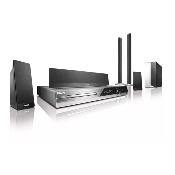
DVD Hometheatre System
Service
Service Manual
©
Copyright 2007 Philips Consumer Electronics B.V. Eindhoven, The Netherlands
All rights reserved. No part of this publication may be reproduced, stored in a retrieval system or
transmitted, in any form or by any means, electronic, mechanical, photocopying, or otherwise
without the prior permission of Philips.
Published by KC-ET741 Service Audio Printed in The Netherlands Subject to modification
Version 1.1
TABLE OF CONTENTS
Location of PC Boards ................................................ 1-2
Versions Variation & Package .................................... 1-2
Specifications .............................................................. 1-3
Service Aids ................................................................ 1-4
ESD & Safety Instruction ............................................ 1-5
Lead-free solding Information .................................... 1-6
Repair Instructions ......................................................... 2
Disassembly Instructions & Service positions .............. 3
Block & Wiring Diagram ................................................ 4
Scart Board ..................................................................... 5
Control Board ................................................................. 6
Main Board ..................................................................... 7
Power Board .................................................................. 8
Mechanical Exploded View & Parts...............................9
1 - 1
Chapter
HTS3357/
/
12
05
3139 785 32711
Advertisement
Chapters
Table of Contents

Related Manuals for Philips HTS3357/12


Summary of Contents for Philips HTS3357/12
- Page 1 Mechanical Exploded View & Parts.......9 © Copyright 2007 Philips Consumer Electronics B.V. Eindhoven, The Netherlands All rights reserved. No part of this publication may be reproduced, stored in a retrieval system or transmitted, in any form or by any means, electronic, mechanical, photocopying, or otherwise without the prior permission of Philips.
-
Page 2: Location Of Pcb Boards
1 - 2 LOCATION OF PCB BOARDS SCART PCB MAIN PCB STANDBY PCB POWER PCB CONTROL PCB MP3 PCB USB PCB VERSION VARIATION: HTS3357 Type/Versions Features & Board in used Main (Output Power-600W) Composite Video Out Power Voltage (230V) AC Cord (Fix) -
Page 3: Speci Cations
1 - 3 Speci cations AMPLIFIER REAR SPEAKERS Total output power ..........600 W RMS System ............Full range satellite Frequency Response ......150 Hz – 18 kHz / ±3 dB Impedance ................3 Signal-to-Noise Ratio ........> 60 dB (A-weighted) Speaker drivers .........3” full range speaker Input Sensitivity Frequency response ........120 Hz –... - Page 4 1 - 4 SERVICE AIDS Service Tools: Universal Torx driver holder .........4822 395 91019 Torx bit T10 150mm ...........4822 395 50456 Torx driver set T6-T20 .........4822 395 50145 Torx driver T10 extended ........4822 395 50423 Compact Disc: SBC426/426A Test disc 5 + 5A ......4822 397 30096 SBC442 Audio Burn-in test disc 1kHz ....4822 397 30155 SBC429 Audio Signals disc .........4822 397 30184 Dolby Pro-logic Test Disc ........4822 395 10216...
- Page 5 1 - 5 WAARSCHUWING WARNING Alle IC’s en vele andere halfgeleiders zijn All ICs and many other semi-conductors are gevoelig voor electrostatische ontladingen susceptible to electrostatic discharges (ESD). (ESD). Careless handling during repair can reduce life Onzorgvuldig behandelen tijdens reparatie kan drastically.
- Page 6 Due to lead-free technology some rules have to be Philips-sets respected by the workshop during a repair: You will find this and more technical information Use only lead-free solder alloy Philips SAC305 with • within the “magazine”, chapter “workshop news”. order code 0622 149 00106. If lead-free solder-paste...
-
Page 7: Repair Instructions
2 - 1 2 - 1 REPAIR INSTRUCTION (Part One) MAIN UNIT REPAIR CHART 1/3 Power Supply All Function Ipod input Audio line IN Wireless COAXIAL In All Function DVD Audio MP3 In Tuner No Sound No Svideo Output HDMI No Output No CVBS Output No Y Pr Pb output KARAOKE In... - Page 8 2 - 2 2 - 2 REPAIR INSTRUCTION (Part Two) MAIN UNIT REPAIR CHART 2/3 AUX/TV IN DVD Audio Ipod input Check IC801 NO SCART OUTPUT No Output No Sound And Its conjoint parts No Sound Check CN802 CN803 Check JK302 Check Open/Close Check DOCK TO Change this jk...
- Page 9 2 - 3 2 - 3 REPAIR INSTRUCTION (Part Three) MAIN UNIT REPAIR CHART 3/3 Tuner No Sound Check SW Power HDMI No Output NO SCART OUTPUT Output See B FM Function No Sound Check CN301Q901 ZD904 Check CN302 IC301 Insert And Pull out HDMI CheckQ610 Q611 Q609 Check CN301 Pin9= +9V...
-
Page 10: Scart Board
3 - 1 3 - 1 DISASSEMBLY INSTRUCTIONS 2) Return the set to its upright position and remove the Tray Dismantling of the Main PCB Cover as shown in Figure 3 and close the tray manually by 2) Loosen 3 screw “ A “ on the top of main board as shown in pushing it back in. -
Page 11: Control Board
3 - 2 3 - 2 Dismantling of the Control Board SERVICE POSITIONS 1) Loosen 10 screws “E” on the top of control board as shown in gure 6 Service position A Figure 6 Dismantling of the Power Board Dismantling of the DVD Module 1) Loosen 5 screws “D”... - Page 12 4 - 1 4 - 1 BLOCK DIAGRAM PHONE JACK SP DIF IN IC MP3-IN TV-I N AUX-IN SIRIUS SA TELLI TE RADIO USB SOCKET CS8415 COAXIAL INPUT IC TC4051BPx 2 SWITCH S-VIDEO AMPLIFIER AMPLIFIER Panasonic TUNER MT1389HD u_co m C-VIDEO SYSTEM IC IRC4558...
- Page 13 4 - 2 4 - 2 WIRING DIAGRAM COAXIAL IN...
- Page 14 5 - 1 SCART BOARD TABLE OF CONTENTS Circuit Diagram & PCB Layout Top ........... 5-2...
- Page 15 5 - 2 CIRCUIT DIAGRAM C710 C712 C714 FB707 FB709 FB711 JK703 R708 RB702 A2 C711 C713 C715 FB708 FB710 FB714 R707 RB701 A1 JK703 SCART FB711 R707 1K SCART_R C710 4.7U FB710 R708 1K SCART_L 4.7U C711 AGND RB702 C715 100P BGND RB701...
- Page 16 6 - 1 6 - 1 FTD DISPLAY PIN ASSIGNMENT CONTROL BOARD TABLE OF CONTENTS FTD Display Pin Assignment ............. 6-1 Voltage ....................6-2 Circuit Diagram .................. 6-3 PCB Layout Top & Bottom View ............6-4 Note...
- Page 17 6 - 2 6 - 2 VOLTAGE IC251 Pin NO Voltage 4.70 -23.00 -26.00 -23.00 -23.00 -21.00 -21.00 -23.00 -23.00 -21.00 -21.00 -23.00 -23.00 -23.00 -26.00 -21.00 -26.00 -26.00 -23.00 4.70 Pin NO Voltage -26.00 -23.00 -23.00 -22.00 -22.00 -24.00 -24.00 -24.00 -24.00 -24.00 -24.00 4.70 4.70 0.00...
- Page 18 6 - 3 6 - 3 CIRCUIT DIAGRAM C2501 A3 C2509 A2 C2515 B1 C2522 B1 C2528 A1 C2540 B2 D2507 B1 FB35 JMP11 B3 JMP5 LD2501 B3 R2503 A1 R2509 A1 R2517 B1 R2523 B1 R2530 A1 R2540 A1 R2549 A1 RB903 A1 TA2507 B1...
- Page 19 6 - 4 6 - 4 PCB LAYOUT - TOP VIEW C2504 C2531 D2504 JMP1 JMP14 JMP3 JMP7 R2502 R2528 R2540 RB5501 A3 SN251 TA2506 B1 TA2511 B1 XL2501 B2 C2505 D2501 D2507 JMP11 JMP15 JMP5 JMP8 R2508 R2532 RB201 RB903 TA2501 A3 TA2507 B1...
-
Page 20: Table Of Contents
7 - 1 7 - 1 INTERNAL IC DIAGRAM - CO4558A HOSP MAIN BOARD TABLE OF CONTENTS Internal IC Diagram ................7-1 Circuit Diagram (Ampli er) ..............7-2 Circuit Diagram (Servo) ..............7-3 PCB Layout Top View ............... 7-4 PCB Layout Bottom View ..............7-5 Voltage .................... -
Page 21: Circuit Diagram (Ampli Er)
7 - 2 7 - 2 Circuit Diagram (Ampli er) C0101 C522 C941 L504 R438 R938 C0102 C523 C942 L507 R439 R939 C0103 C524 C943 L508 R440 R940 C0104 C526 C944 L510 R441 R941 C0105 C527 C945 L511 R442 R942 C0106 C528 C947... -
Page 22: Circuit Diagram (Servo)
7 - 3 7 - 3 Circuit Diagram (Servo) C0201 C231 CN202 C1 R223 R826 C0202 C232 CN203 D4 R224 R827 C0203 C233 CN802 B1 R225 R828 C0204 C234 CN803 B1 R227 R829 C0205 C235 D201 R228 R830 C0206 C236 D202 R230 R831... -
Page 23: Pcb Layout Top View
7 - 4 7 - 4 PCB Layout Top View C0114 D2 C109 C243 C363 C507A B1 C579 C722 C828 C920 CN702 A4 D707 FB302 C5 FB802 D5 L207 Q300 Q910 R224 R261 R322 R361 R434 R511 R611 R808 R907 R945 C0115 A3 C201... -
Page 24: Pcb Layout Bottom View
7 - 5 7 - 5 PCB Layout Bottom View C0101 C0112 C0209 C0226 C0242 C0502 C0609 C228 C320 C5002 C550 C569 C601 C821 C908 CE201 CE501 CE511 CN201 D4 D912 R220 R393 R521 R572 R921 C0102 C0113 C0210 C0228 C0243 C0504 C0612... -
Page 25: Voltage
7 - 6 7 - 6 VOLTAGE IC201 IC301 Pin NO Pin NO Voltage 0.00 0.00 0.00 -13.00 0.00 0.00 0.00 12.00 Voltage 3.30 0.00 0.00 2.50 2.50 5.10 0.00 0.00 3.30 2.50 5.10 1.80 0.00 0.00 0.00 5.00 5.00 0.00 5.00 0.00 Pin NO... -
Page 26: Voltage
8 - 1 8 - 1 VOLTAGE IC901 Pin NO Voltage 4.80 4.80 2.40 0.00 1.70 3.40 0.00 12.00 2.30 2.30 12.00 12.00 4.90 4.90 2.40 0.00 IC902 Pin NO Voltage 2.70 0.00 0.50 2.10 0.00 1.00 11.00 4.90 IC903 Pin NO Voltage 4.90... -
Page 27: Circuit Diagram
8 - 2 8 - 2 CIRCUIT DIAGRAM BD901 A1 C913 C925 C935 C946 C957 C967 CN903 A5 D910 D921 IC903 L906 Q910 R903 R916 R926A A5 R937 R949 R961 R971 R981 R991 ZD902 A4 ZD913 C1 C901 C914 C926 C937 C948 C958... -
Page 28: Pcb Layout Top View
8 - 3 8 - 3 PCB LAYOUT - TOP VIEW BD901 C916 C937 C949 C955 C963 C971 CN905 D918 D924 IC903 J910 J916 J924 J930 L901 L907 Q908 Q914 R906 R936 R942 R961 R984 T903 ZD908 C901 C920 C938 C950 C956 C964... -
Page 29: Pcb Layout Bottom View
8 - 4 8 - 4 PCB LAYOUT - BOTTOM VIEW C904 B3 C911 A2 C925 C2 C930 C2 C941 C3 C959 B2 D901 B3 D910 B3 Q906 C1 R911 B1 R920 B1 R925 C1 R929 A4 R947 B1 R955 C1 R963 C2 R972 C2 R977 B1... - Page 30 9 - 1 9 - 1 Mechanical Exploded View note: A1=14+30+31+32+33...
- Page 31 MECHANICAL PART LIST Main Unit Speaker LOC. PART NO. Description LOC. PART NO. Description 996510001254 DISPLAY LENS SPKC 996510009246 SPEAKER BOX -CENTER 996510001661 FRONT ASSY SPKFL 996510009247 SPEAKER BOX -FRONT LEFT 996510001256 STANDY BUTTON SPKFR 996510009248 SPEAKER BOX - FRONT RIGHT 996510001257 OPEN/CLOSE BUTTON SPKRL...