Table of Contents
Advertisement
Quick Links
HDD & DVD Recorder
CLASS 1
LASER PRODUCT
Contents
1
Technical Specifications and Connection
Facilities
2
Safety Information, General Notes & Lead
Free Requirements
3
Directions for Use
4
Mechanical Instructions
5
Firmware Upgrading & Diagnostic Software
6
Block Diagrams,Waveforms, Wiring Diagram
Overall block diagram
Wiring diagram
Waveforms of Analog Board
Waveforms of Digital Board
Waveforms of HDMI Board
Test Points Overview for Analog Board
Test Points Overview for Front Left Board
Test Points Overview for Front Right Board
Test Points Overview for
Front AV_INPUT Board
Test Points Overview for Digital Board
Test Points Overview for HDMI Board
Test Points Overview for IR Blaster Board
© Copyright 2005 Philips Consumer Electronics B.V. Eindhoven, The Netherlands.
All rights reserved. No part of this publication may be reproduced, stored in a
retrieval system or transmitted, in any form or by any means, electronic,
mechanical, photocopying, or otherwise without the prior permission of Philips.
Published by KC-TE 0547 AV Systems
Version 1.1
Contents
Page
7
2
5
7
10
14
131
131
132
133
134
135
8
9
136
137
138
10 Exploded view & Service parts list
139
140
11 Revision List
141
142
Printed in the Netherlands
DVDR9000H/10/75/97
Circuit Diagrams and PWB Layout
Analog Circuit Diagrams
Analog Layout Diagrams
PCB Front Circuit Diagrams
PCB Front Layout Diagrams
Digital Circuit Diagrams
Digital Layout Diagrams
HDMI Circuit Diagrams
IR Blaster Board Circuit Diagrams
IR Blaster Board Layout Diagrams
DTTM Circuit Diagrams
DTTM Component Diagrams
Alignments & Test Procedures
Circuit and IC description
Circuit Description
IC Description
Exploded View of the set
Service parts list
Subject to modification
Page
143
143
153
155
158
161
172
174
178
179
180
186
189
190
190
199
238
238
239
240
EN 3139 785 31681
Advertisement
Table of Contents

Related Manuals for Philips DVDR9000H/75


Summary of Contents for Philips DVDR9000H/75
- Page 1 Test Points Overview for HDMI Board Test Points Overview for IR Blaster Board © Copyright 2005 Philips Consumer Electronics B.V. Eindhoven, The Netherlands. All rights reserved. No part of this publication may be reproduced, stored in a retrieval system or transmitted, in any form or by any means, electronic, mechanical, photocopying, or otherwise without the prior permission of Philips.
-
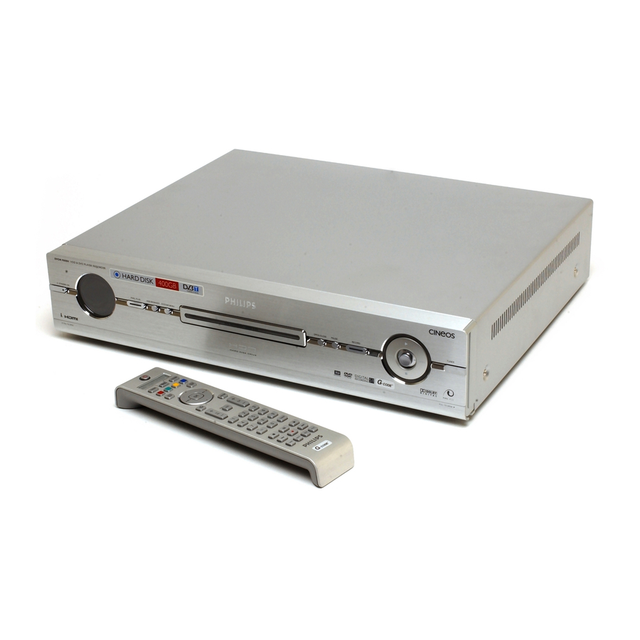
Page 2: Technical Specifications And Connection Facilities
Read / Write Speed 1.4.1.4 Video Performance: Channel 25 / 503,25 MHz, Type of Disc (Function) Disc Rotation Speed Test pattern: PAL BG PHILIPS standard test pattern, RF Level 74dBV, Measured on SCART 1 Read Speed CD 7X CAV Frequency response : 0.1 MHz –... - Page 3 Technical Specifi cations and Connection Facilities 3139 785 31681 EN 3 1.4.2 RF Tuner (Digtal Terrestial) 1.5.2 SCART 2 (Connected to AUX) Pin Signals: 1.4.2.1 DVB - T - Tuner Audio-out R 1.8V RMS Frequency range : 49-861MHz Audio-in R Gain (ANT IN –...
- Page 4 EN 4 3139 785 31681 Technical Specifi cations and Connection Facilities Digital Inputs / Outputs Dimensions and Weight Height of feet : 5.5mm 1.6.1 Digital Output Apparatus tray closed : WxDxH:435x390x89mm Apparatus tray open : WxDxH:435x525x89mm Digital Audio – Coaxial / Optical Weight without packaging : approx.
-
Page 5: Safety Information, General Notes & Lead Free Requirements
Safety Information, General Notes & Lead Free Requirements 3139 785 31681 EN 5 Safety Information, General Notes & Lead Free Requirements Safety Instructions Warnings 2.1.1 General Safety 2.2.1 General Safety regulations require that during a repair: • All ICs and many other semiconductors are susceptible to •... - Page 6 • On our website www.atyourservice.ce.Philips.com you fi nd more information to: BGA-de-/soldering (+ baking instructions) Heating-profi les of BGAs and other ICs used in Philips-sets You will fi nd this and more technical information within the “magazine”, chapter “workshop news”.
-
Page 7: Directions For Use
Directions For Use The following except of the Quick Use Guide serves as an introduction to the set. The Complete Direction for the Use can be downloaded in different languages from the internet site of Philips Customer care Center: www.p4c.philips.com... - Page 8 EN 8 3139 785 31681 Directions For Use...
- Page 9 Directions For Use 3139 785 31681 EN 9...
-
Page 10: Mechanical Instructions
EN 10 3139 785 31681 Mechanical Instructions Mechanical Instructions Note: The position numbers given here refers to the Exploded view on chapter 10. 3) Remove 2 screws to loosen the Bracket Loader 191 and Dismantling of the DVD Tray cover manually uncatch the Dust cover assembly 902. - Page 11 Mechanical Instructions 3139 785 31681 EN 11 2) Remove 4 screws 285 to separate the Bracket HDD 4) Service position for PSU Board is given in Figure 4-8. 192 and Bracket HDD suspension 222 from the HDD as shown in Figure 4-6. Note: Screws 285 are special type of screws that must be replaced only with those specifi...
- Page 12 EN 12 3139 785 31681 Mechanical Instructions 2) Service position for Digital Board is given in Figure 2) Remove 8 screws to loosen the Analog Board (3x) and 4-10. IR Blaster board (2x) + bracket 193 assembly (3x) as shown in Figure 4.12. Insulation Sheet Figure 4-10: Digital Board Service Position Figure 4-12...
- Page 13 Mechanical Instructions 3139 785 31681 EN 13 4) Service Position is achieved by placing the Analog Board in the vertical position as shown in Figure 4-14. Insulation Sheet Insulation Sheet Figure 4-14: HDMI and Analog Boards Service Position Dismantling of the Front Panel assembly 1) Remove the DVD Tray cover assembly 910 as given in step 4-1.
-
Page 14: Firmware Upgrading & Diagnostic Software
EN 14 Firmware Upgrading & Diagnostic Software 3139 785 31681 Firmware Upgrading & Diagnostic Software Firmware Upgrading A. Preparation to upgrade fi rmware: 1. Unzip the zip-archive fi le 2. Start the CD Burning software and create a new CD project (data disc) with the following settings: File system: Joliet Format:... - Page 15 Firmware Upgrading & Diagnostic Software 3139 785 31681 EN 15 Diagnostic Software Due to the complexity of the DVD recorder, the time to find a 5.2.2 Structure defect in the recorder can become long. To reduce this time, the recorder has been equipped with Diagnostic and Service software (DS).
- Page 16 EN 16 Firmware Upgrading & Diagnostic Software 3139 785 31681 Player Script Interface Virgin mode 5.3.1 5.4.2 Error Handling If you want that the recorder starts up in Virgin mode, follow this Each nucleus returns an error code. This code contains six procedure: numerals, which means: •...
- Page 17 Firmware Upgrading & Diagnostic Software 3139 785 31681 EN 17 3. It is possible that the next messages will appear when Enter "Y" to program a safe string. With this automatically starting the DVD+RW for the first time generated string the board will work in principle but it has to be checked if all board settings were detected correctly.
- Page 18 EN 18 Firmware Upgrading & Diagnostic Software 3139 785 31681 Command overview Digital Board Below you will find an overview of the nuclei, their numbers, and their error codes. This overview is preliminary and subject to modifications. Note: AV3 in the overview includes also the AV3.5 drive. Codec Host Controller (CHR) DS_CHR_DevTypeGet Nucleus Name...
- Page 19 Firmware Upgrading & Diagnostic Software 3139 785 31681 EN 19 User Input The user has to decide which test image, video standard and video output must be used: < Test image id > < Video standard > < Video output > Test image id: VERTICAL_COLOURBAR (default) HORIZONTAL_COLOURBAR...
- Page 20 EN 20 Firmware Upgrading & Diagnostic Software 3139 785 31681 DS_CHR_SineOn Nucleus Name Nucleus Number Description Generate an audio sine signal on the audio output of the digital board. Note: Left channel 6kHz, right channel 12 kHz sine. Make sure to route the signal first.
- Page 21 Firmware Upgrading & Diagnostic Software 3139 785 31681 EN 21 DS_CHR_MuteOn Nucleus Name Nucleus Number Description Mute the audio outputs of the digital board Technical Send the ‘Mute’ command to the audio decoder Activate the ‘audio mute’ PIO pin Execution Time Less than 1 second.
- Page 22 EN 22 Firmware Upgrading & Diagnostic Software 3139 785 31681 DS_CHR_MacroVisionOn Nucleus Name Nucleus Number Description Turn on MacroVision. Technical Set some registers of the DENC module in the Codec. Execution Time Less than 1 second. User Input None Error Number Description 11000...
- Page 23 Firmware Upgrading & Diagnostic Software 3139 785 31681 EN 23 DS_CHR_INT_PICInterrupts Nucleus Name Nucleus Number Description Test all interrupts of the priority interrupt controller Technical Install interrupt handlers Generate interrupts Test whether all interrupts were received Execution Time Less than 1 second. User Input Error Number...
- Page 24 EN 24 Firmware Upgrading & Diagnostic Software 3139 785 31681 DS_BROM_WriteRead Nucleus Name Nucleus Number Description Check whether the Boot EEPROM can be written to and read from Technical Initialise IIC Write something to the EEPROM Read from the same location and check whether it is the same as written Execution Time Less than 1 second.
- Page 25 Firmware Upgrading & Diagnostic Software 3139 785 31681 EN 25 DS_NVRAM_Clear Nucleus Name Nucleus Number Description Make the EEPROM empty, containing all zeroes. Technical Initialise IIC If no IIC EEPROM was found then initialise flash memory to use NVM pages Read the DVID and diversity string from NVM (either EEPROM or Flash) Create a memory block filled with zeroes Write this block to the NVRAM (either EEPROM or Flash)
- Page 26 EN 26 Firmware Upgrading & Diagnostic Software 3139 785 31681 DS_NVRAM_Read Nucleus Name Nucleus Number Description Read out one or more locations in the NVRAM Technical Initialise IIC If no IIC EEPROM was found then initialise flash memory to use NVM pages Decode user input Read from the NVRAM and return this info to the user...
- Page 27 Firmware Upgrading & Diagnostic Software 3139 785 31681 EN 27 DS_SDRAM_Write Nucleus Name Nucleus Number Description Write to a specific un-cached memory address Technical Decode the user input and check its ranges and alignment on 4 bytes Write the data to the SDRAM Execution Time Less than 1 second User Input...
- Page 28 EN 28 Firmware Upgrading & Diagnostic Software 3139 785 31681 FLASH (FLASH) DS_FLASH_DevTypeGet Nucleus Name Nucleus Number Description Get the device (revision) type information of the FLASH ICs. (type, manufacturer, device ID and size) Technical Set the timing for the flash writing Write a command sequence to determine device type information Return the information to the user Execution Time...
- Page 29 Firmware Upgrading & Diagnostic Software 3139 785 31681 EN 29 DS_FLASH_ChecksumProgram Nucleus Name Nucleus Number Description Check the checksum of the application partitions by recalculating and comparing partition checksums Technical Determine the number of segments Find the application in each segment and determine its checksum Check whether the checksums stored match the newly calculated Execution Time 6 seconds...
- Page 30 EN 30 Firmware Upgrading & Diagnostic Software 3139 785 31681 DS_VIP_Communication Nucleus Name Nucleus Number Description Check the communication between the IIC controller of the Codec and the VIP Technical Initialise IIC Read data from a location in the VIP Execution Time Less than 1 second User Input...
- Page 31 Firmware Upgrading & Diagnostic Software 3139 785 31681 EN 31 DS_VIP_SelectInput Nucleus Name Nucleus Number Description Select an input video path to be switched to the analogue output pin (AOUT) of the VIP Technical Check the user input Initialise IIC Read out the VIP id Write the set of registers required for the input specified Execution Time...
- Page 32 EN 32 Firmware Upgrading & Diagnostic Software 3139 785 31681 Error Number Description 60400 Selecting the input of the VIP succeeded 60401 The user provided wrong input 60402 The VIP was not accessible 60403 An unsupported VIP was found DS:> 604 1 Example 060400: Test OK @...
- Page 33 Firmware Upgrading & Diagnostic Software 3139 785 31681 EN 33 DS_DVIO_PhyCommunication Nucleus Name Nucleus Number Description Check the accessibility of the 1394 Physical layer IC by writing to and reading from a specific address Technical Initialise the PIO pins of the Codec Initialise IIC Write the data to be written to the PHY-chip to the link chip first Wait until the link chip indicates that the data has been written to the PHY...
- Page 34 EN 34 Firmware Upgrading & Diagnostic Software 3139 785 31681 DS_DVIO_DetectStream Nucleus Name Nucleus Number Description Check whether a DV stream can be detected by the hardware. This test works for both NTSC and PAL. Technical Initialise the 1394 interface Start receiving the stream Detect whether the stream is OK Execution Time...
- Page 35 Firmware Upgrading & Diagnostic Software 3139 785 31681 EN 35 DS_PSCAN_TestImageOn Nucleus Name Nucleus Number Description Generate the test images that are present on the progressive scan IC. Technical Determine whether the user wanted a HATCH or a FRAME image pattern Initialise the PIO pins of the Codec Initialise IIC Reset the DENC...
- Page 36 EN 36 Firmware Upgrading & Diagnostic Software 3139 785 31681 DS_PSCAN_TestImageColourSettingsSet Nucleus Name Nucleus Number Description Set the colour of the hatch- or the frame- field to a different value than the default white Technical Determine which colour must be set. Initialise IIC.
- Page 37 Firmware Upgrading & Diagnostic Software 3139 785 31681 EN 37 DS_PSCAN_DevTypeGetDeinterlacer Nucleus Name Nucleus Number Description See nucleus 800. DS:> 807 Example 080700: Chip name : 2300 Chip version : 1 Test OK @ DS_PSCAN_CommunicationDeinterlacer Nucleus Name Nucleus Number Description See nucleus 801.
- Page 38 The BE returned no info DS:> 903 Example (AV2) 090300: BE version = 20.09.18 Optical unit version = 3C.00.09.41.08 Test OK @ DS:> 903 Example (AV3) 090300: BE version = 31.30.24. PHILIPS ,VAD8031 ,31302400,REL_8031_313024 2073, Optical unit version = 00.06.82.19.00 Test OK @...
- Page 39 Firmware Upgrading & Diagnostic Software 3139 785 31681 EN 39 DS_BE_TrayOut Nucleus Name Nucleus Number Description Open the tray of the basic engine Technical Check if an AV2 or AV3 is connected In case of an AV2 Send the S2B TRAY_OUT command In case of an AV3 send an ATAPI START_STOP_UNIT command Execution Time Approximately 2 seconds...
- Page 40 EN 40 Firmware Upgrading & Diagnostic Software 3139 785 31681 DS_BE_WriteReadDvdRw Nucleus Name Nucleus Number Description Write data to and read data from a DVD+RW disc through the basic engine for verification of the writing Technical Check if an AV2 or AV3 is connected Execute DS_BE_GetSelftestResults Send the TRAY_IN command Send the READ_TOC command...
- Page 41 Firmware Upgrading & Diagnostic Software 3139 785 31681 EN 41 DS_BE_WriteReadDvdR Nucleus Name Nucleus Number Description Write data to and read data from a DVD+R disc through the basic engine for verification of the writing Technical Check if an AV2 or AV3 is connected Execute DS_BE_GetSelftestResults Send the TRAY_IN command Send the READ_TOC command...
- Page 42 EN 42 Firmware Upgrading & Diagnostic Software 3139 785 31681 DS_BE_StatisticalInformationGet Nucleus Name Nucleus Number Description Retrieve the statistical information from the basic engine Technical Check if an AV2 or AV3 is connected In case of an AV2 Send the S2B GET_STATISTICAL_INFO command In case of an AV3 Send the transparent BIT engine GET_STATISTICAL_INFO command Display the info returned from the BE...
- Page 43 Firmware Upgrading & Diagnostic Software 3139 785 31681 EN 43 DS_BE_StatisticalInformationReSet Nucleus Name Nucleus Number Description Reset the statistical information in the basic engine Technical Check if an AV2 or AV3 is connected In case of an AV2 Send the S2B RESET_STATISTICAL_INFO command Send the S2B POWER_DOWN command Toggle the reset pin of the I2S interface In case of an AV3 Send the transparent BIT engine...
- Page 44 EN 44 Firmware Upgrading & Diagnostic Software 3139 785 31681 DS_BE_ErrorLogReset Nucleus Name Nucleus Number Description Reset the error log in the basic engine Technical Check if an AV2 or AV3 is connected In case of an AV2 Send theS2B RESET_STATISTICAL_INFO command Send the S2B POWER_DOWN command Toggle the reset pin of the I2S interface In case of an AV3 Send the transparent BIT engine...
- Page 45 Firmware Upgrading & Diagnostic Software 3139 785 31681 EN 45 DS_BE_FocusOn Nucleus Name Nucleus Number Description Put the laser of the BE into focus Technical Check if an AV2 or AV3 is connected In case of an AV2 Send the FOCUS command with parameter 0x01 In case of an AV3 Send the transparent BIT engine FOCUS command Execution Time 3 seconds...
- Page 46 EN 46 Firmware Upgrading & Diagnostic Software 3139 785 31681 DS_BE_MotorOff Nucleus Name Nucleus Number Description Turn off the turntable motor Technical Check if an AV2 or AV3 is connected In case of an AV2 Send the TURN_TABLE_MOTOR_OFF command In case of an AV3 Send the transparent BIT engine TTM command Execution Time Less than 1 second on AV2 4 seconds on AV3...
- Page 47 Unable to load the tray 92102 Error received from BE DS:> 921 Example 092100: Disc type: DVD+RW disc Disc manufacturer id: PHILIPS Media type id: 010 Test OK @ DS:> 921 090500: Disc type: None Test OK @ DS:> 921...
- Page 48 EN 48 Firmware Upgrading & Diagnostic Software 3139 785 31681 DS_BE_ReadTocInfo Nucleus Name Nucleus Number Description Read the TOC from the disc. This gives a good indication if the BE works properly. Technical Send the TRAY_IN command Send the READ_TOC command Display the TOC info.
- Page 49 Firmware Upgrading & Diagnostic Software 3139 785 31681 EN 49 DS_BE_RegionCodeSet Nucleus Name Nucleus Number Description Set the region code in the AV3. Technical Check if an AV2 or AV3 is connected In case of anAV2 display a “not supported” message In case of an AV3 send the ATAPI SEND_KEY command Execution Time User Input...
- Page 50 EN 50 Firmware Upgrading & Diagnostic Software 3139 785 31681 DS_BE_RegionCounterReset Nucleus Name Nucleus Number Description Reset the region counter in the AV3. Technical Check if an AV2 or AV3 is connected In case of an AV2 display a “not supported” message In case of an AV3 send a special ATAPI RESET_REGION_COUNTER command Execution Time...
- Page 51 Firmware Upgrading & Diagnostic Software 3139 785 31681 EN 51 Nucleus Name DS_BE_WriteReadDvdRDualLayer Nucleus Number Description Write data to and read data from both layers of a DVD+R DL disc through the basic engine for verification of the writing Technical Send the TRAY_IN command Send the READ_TOC command Use READ_TRACK_INFORMATION to determine the next free writable...
- Page 52 EN 52 Firmware Upgrading & Diagnostic Software 3139 785 31681 System (SYS) DS_SYS_HardwareVersionGet Nucleus Name Nucleus Number 1200 Description Get the hardware version and type of the digital board Technical Initialise the PIO pins of the Codec Read the segment header in FLASH and determine hardware version Execution Time Less than 1 second User Input...
- Page 53 Firmware Upgrading & Diagnostic Software 3139 785 31681 EN 53 DS_SYS_SoftwareVersionDiagnosticsGet Nucleus Name Nucleus Number 1204 Description Get the version of the diagnostics software on the digital board Technical Read the segment header in FLASH and determine Diagnostics software version Execution Time Less than 1 second User Input...
- Page 54 EN 54 Firmware Upgrading & Diagnostic Software 3139 785 31681 DS_SYS_EepromDownload Nucleus Name Nucleus Number 1206 Description Download a file with the contents of the NVRAM for the analogue board or the digital board from the service PC to the recorder, by using the X-modem protocol Technical Decode the user input and determine what EEPROM to fill: digital /...
- Page 55 Firmware Upgrading & Diagnostic Software 3139 785 31681 EN 55 DS_SYS_IicWrite Nucleus Name Nucleus Number 1209 Description Perform an IIC write action on the digital board Technical Determine bus ID, slave address, number of bytes to be written and the byte array of data from the user input Initialise IIC Write the data to the slave specified through IIC...
- Page 56 EN 56 Firmware Upgrading & Diagnostic Software 3139 785 31681 Nucleus Name DS_SYS_UartWrite Nucleus Number 1211 Description Perform an UART write action on the digital board on a specified UART Technical Decode the user input for the proper port to use Write out the bytes through the indicated port Execution Time Less than 1 second.
- Page 57 Firmware Upgrading & Diagnostic Software 3139 785 31681 EN 57 User Input <vipInput> <VideoOutput> <VideoStandard> vipInput (see table below). GEN, OLAX, DXC, DTT specific User input Video input Data path to VIP CVBS CVBS from analogue board YC from analogue board CVBS YUV from analogue...
- Page 58 EN 58 Firmware Upgrading & Diagnostic Software 3139 785 31681 DS_SYS_VideoLoopThroughStop Nucleus Name Nucleus Number 1214 Description Stop routing the video input to all the outputs. Technical Stop the DENC and the Video Front End Execution Time Less than 1 second. User Input None Error...
- Page 59 Firmware Upgrading & Diagnostic Software 3139 785 31681 EN 59 User Input <vipinput> <video standard> 1 Vip input of the digital board: GEN, OLAX, DXC, DTT specific User input Video input Data path to VIP CVBS CVBS from analogue board YC from analogue board CVBS...
- Page 60 EN 60 Firmware Upgrading & Diagnostic Software 3139 785 31681 121510 When selected the RGB video input: Error in colour red signal and/or Error in colour green signal and/or Error in colour blue signal. When selected one of the other video inputs: Error in luminance signal (Y) and/or Error in chrominance signal (U) and/or Error in chrominance signal (V).
- Page 61 Firmware Upgrading & Diagnostic Software 3139 785 31681 EN 61 DS:> 1216 Example 121600: Test OK @ DS:> 1216 spdif coax 121600: Test OK @ DS:> 1216 spdif opt 121600: Test OK @ DS_SYS_SlashVersionSet Nucleus Name Nucleus Number 1217 Description Set the slash version of the system Technical Decode the user input for the slash version to set...
- Page 62 EN 62 Firmware Upgrading & Diagnostic Software 3139 785 31681 DS_SYS_Virginize Nucleus Name Nucleus Number 1219 Description (Re-) Virginize the recorder. User data in the NVRAM of the analogue board is cleared Technical Issue the command to return to the factory defaults to the analogue board Execution Time 1 second.
- Page 63 Firmware Upgrading & Diagnostic Software 3139 785 31681 EN 63 DS_SYS_VirginModeGet Nucleus Name Nucleus Number 1222 Description Get the virgin mode functionality status (e.g. the auto channel search upon start-up) Technical Issue the command to reset the bit for the virgin mode to the analogue board Execution Time Less than 1 second.
- Page 64 EN 64 Firmware Upgrading & Diagnostic Software 3139 785 31681 DS_SYS_DisplayFatalGet Nucleus Name Nucleus Number 1225 Description Get the display-fatal flag of the recorder Technical Issue the command to get the status of the display-fatal functionality to the analogue board Execution Time Less than 1 second.
- Page 65 Firmware Upgrading & Diagnostic Software 3139 785 31681 EN 65 DS_SYS_SettingsDisplay Nucleus Name Nucleus Number 1228 Description Show the settings that are programmed in the BROM on the digital board. Technical Set-up IIC-bus. Read Digital Board Settings from boot EEPROM. Display the settings.
- Page 66 EN 66 Firmware Upgrading & Diagnostic Software 3139 785 31681 DS_SYS_AudioLoopThroughStart Nucleus Name Nucleus Number 1230 Description Description: The audio input is routed from the input to all outputs. The input is set routing the signal with the proper nucleus. All outputs are enabled. Technical Encode the audio to AC3 in memory Decode the AC3 in memory to audio on the outputs...
- Page 67 Firmware Upgrading & Diagnostic Software 3139 785 31681 EN 67 DS_SYS_SettingsHwIdSet Nucleus Name Nucleus Number 1232 Description This nucleus sets the HW-Id in the HW-diversity string Technical Read out the HW-diversity string Modify the HW-ID in that string as requested Write the modified HW-diversity string to the EEPROM Execution Time Less than 1 second.
- Page 68 EN 68 Firmware Upgrading & Diagnostic Software 3139 785 31681 DS_SYS_SettingsDoubleCheck Nucleus Name Nucleus Number 1233 Description Double check whether stored HW-string equals actual HW as far as we can automatically detect this. An automatic and a manual mode is supported.
- Page 69 Firmware Upgrading & Diagnostic Software 3139 785 31681 EN 69 DS_SYS_SettingsDlTableFilenameSet Nucleus Name Nucleus Number 1234 Description This nucleus sets the Download table filename in the HW-diversity string Technical Retrieve the new filename from the user Ask the user whether the filename is correct before setting it Update the diversity settings to use the newly entered filename Execution Time Dependent on the user confirmation...
- Page 70 EN 70 Firmware Upgrading & Diagnostic Software 3139 785 31681 DS_SYS_BuildInfoGet Nucleus Name Nucleus Number 1236 Description Retrieve the software build information of the Diagnostics & Service application Technical Show the information that is stored in the DVDR_BuildInfoType structure Execution Time Less than 1 second User Input None...
- Page 71 Firmware Upgrading & Diagnostic Software 3139 785 31681 EN 71 DS_SYS_GLinkWriteRead Nucleus Name Nucleus Number 1238 Description Send out some data through the G-Link UART and read back the data. The user must short-circuit the TX and RX line of the G-Link connector. Technical UART 3 setup (1200, 8, n, 1) Send “HELLO”.
- Page 72 EN 72 Firmware Upgrading & Diagnostic Software 3139 785 31681 Nucleus Name DS_HDMI_Communication Nucleus Number 1501 Description Check the communication between the I2C controller on the Codec and the HDMI-IC by reading and writing data to one device register. This test detects faults of the I2C lines or a defected HDMI transmitter IC.
- Page 73 Firmware Upgrading & Diagnostic Software 3139 785 31681 EN 73 DS_HDMI_EdidParse Nucleus Name Nucleus Number 1502 Description Return the E-EDID (Enhanced Extended Display Identification Data) contained in the HDMI / DVI able TV attached to the DVD+RW. Parse the information retrieved to print the capabilities of the TV in user understandable format Technical Read out the E-EDID through the DDC channel (IIC)
- Page 74 EN 74 Firmware Upgrading & Diagnostic Software 3139 785 31681 Nucleus Name DS_HDMI_DefaultVideoSet Nucleus Number 1503 Description Set a default video configuration in the HDMI TX chip (720x480p) Technical Write a known configuration for 720x480P in the registers of the HDMI transmitter chip Execution Time Less than 1 second.
- Page 75 Firmware Upgrading & Diagnostic Software 3139 785 31681 EN 75 Nucleus Name DS_HDMI_DdcIicWrite Nucleus Number 1506 Description Perform an IIC write action to a device on the DDC bus Technical Execution Time Less than 1 second. User Input <TimeOut> <Slave address> <offset> <nr of bytes> <d1> <.> <dx> Error Number Description...
- Page 76 EN 76 Firmware Upgrading & Diagnostic Software 3139 785 31681 Nucleus Name DS_HDMI_ExtendedWrite Nucleus Number 1508 Description Perform an IIC write action on port 0/1 of the HDMI transmitter Technical Execution Time Less than 1 second. User Input <Port> <Register> <Data> Where 0 == Port 0 and 1 == Port 1 Error Number Description...
- Page 77 Firmware Upgrading & Diagnostic Software 3139 785 31681 EN 77 Nucleus Name DS_HDMI_CheckHPDChrysalis Nucleus Number 1511 Description Check whether Hot-Plugging of the HDMI cable is detected by the software. This tests the interrupt line to the Chrysalis. Technical Execution Time Less than 1 second.
- Page 78 EN 78 Firmware Upgrading & Diagnostic Software 3139 785 31681 Nucleus Name DS_HDMI_FLI2310_TestImageOn Nucleus Number 1514 Description Generate a test image using the FLI2310 Technical Execution Time Less than 1 second. User Input None Error Number Description 151400 Test image is generated successfully 151401 Failed to retrieve the hardware diversity string 151402...
- Page 79 Firmware Upgrading & Diagnostic Software 3139 785 31681 EN 79 Nucleus Name DS_HDMI_FLI2310_ExtendedWrite Nucleus Number 1517 Description Write to any register of the FLI2310 Technical Execution Time Less than 1 second. User Input <Register> <RegLen:1=8bits;2=16bits> <Data> Error Number Description 151700 The IIC write action succeeded 151701 Failed to retrieve the hardware diversity string...
- Page 80 EN 80 Firmware Upgrading & Diagnostic Software 3139 785 31681 Nucleus Name DS_HDMI_Adv7302_Communication Nucleus Number 1520 Description Test whether communication with the ADV7320 can be established Technical Execution Time Less than 1 second. User Input None Error Number Description 152000 Something is properly written so the communication is OK 152001 Failed to retrieve the hardware diversity string...
- Page 81 Firmware Upgrading & Diagnostic Software 3139 785 31681 EN 81 Nucleus Name DS_HDMI_Adv7302_TestImageOff Nucleus Number 1522 Description Switch off test-image generation by the ADV7320 Technical Execution Time Less than 1 second. User Input None Error Number Description 152200 Testimage is turned off successfully 152201 Failed to retrieve the hardware diversity string 152202...
- Page 82 EN 82 Firmware Upgrading & Diagnostic Software 3139 785 31681 Nucleus Name DS_HDMI_Adv7302_ColSettingsGet Nucleus Number 1525 Description Get the colour settings of the hatch- or frame-field Technical Execution Time Less than 1 second. User Input None Error Number Description 152500 Reading the colour settings succeeded 152501 Failed to retrieve the hardware diversity string...
- Page 83 Firmware Upgrading & Diagnostic Software 3139 785 31681 EN 83 Nucleus Name DS_HDMI_Audio Nucleus Number 1528 Description Set the proper audio settings to the HDMI transmitter. Note: When 1528 spdif is used to set the HDMI transmitter audio settings correctly and just 103 is entered i.s.o. 103 spdif then ‘clicking’ audio is heard because the Chrysalis audio decoder does not use its SPDIF-path explicitly.
- Page 84 EN 84 Firmware Upgrading & Diagnostic Software 3139 785 31681 Nucleus Name DS_HDMI_ColumbusPass Nucleus Number 1530 Description Have the Columbus pass the video from its inputs to its outputs Technical Execution Time Less than 1 second. User Input None Error Number Description 153000...
- Page 85 Firmware Upgrading & Diagnostic Software 3139 785 31681 EN 85 DS_ASP_RealTimeClockSetValues Nucleus Name Nucleus Number 1602 Description This nucleus is used to set the real time clock to the correct values. Technical Decode the user input. Write RTC value to ASP. Execution Time Less than 1 second.
- Page 86 EN 86 Firmware Upgrading & Diagnostic Software 3139 785 31681 DS_ASP_NTCGet Nucleus Name Nucleus Number 1606 Description This nucleus reads the value of the NTC-resistor connected to the ASP, which tells the ambient temperature to the processor. Technical Read the ADC input pin of the ASP that is connected to the NTC-resistor. Display this value.
- Page 87 Firmware Upgrading & Diagnostic Software 3139 785 31681 EN 87 DS_ASP_BlinkDisplay Nucleus Name Nucleus Number 1609 Description This nucleus lights the entire display, and lets it blink. Only for ASP Technical Set all segments on in the blink buffer. Set the grids correct in the blink buffer. Send the blink buffer to the ASP.
- Page 88 EN 88 Firmware Upgrading & Diagnostic Software 3139 785 31681 DS_ASP_KeyBoard Nucleus Name Nucleus Number 1612 Description This nucleus checks all keys of the keyboard by having the user confirm the key-code displayed of all keys. If the user presses ‘a’ or ‘A’ the test is aborted. If the user presses ‘o’...
- Page 89 Firmware Upgrading & Diagnostic Software 3139 785 31681 EN 89 DS_ASP_LEDsOn Nucleus Name Nucleus Number 1614 Description Switches on the display leds. Technical ASP specific Check if the analogue board is a MOBO board, if so: Read the ASP pio port. Set the RECORD-LED bit on in this port.
- Page 90 EN 90 Firmware Upgrading & Diagnostic Software 3139 785 31681 DS_ASP_LEDsOff Nucleus Name Nucleus Number 1615 Description This nucleus switches off the display leds. Technical ASP specific Check if the analogue board is a MOBO board, if so: Read the ASP pio port. Set the RECORD-LED bit off in this port.
- Page 91 Firmware Upgrading & Diagnostic Software 3139 785 31681 EN 91 DS_ASP_Watchdog Nucleus Name Nucleus Number 1618 Description This nucleus configures the watchdog timer of the ASP, and waits till the watchdog expires. The watchdog time-out is 10 seconds. On expiry of the watchdog timer, the ASP switching off, and on its power supply, and resets the main controller.
- Page 92 EN 92 Firmware Upgrading & Diagnostic Software 3139 785 31681 DS_ASP_GlinkRcLoop Nucleus Name Nucleus Number 1621 Description Checks if an RC command can be transmitted via the G-Link connector and test if the sent command can be read back. The user must connect the G-Link to the rear G-Link connector and place the RC transmitter in front of the RC receiver of the front panel.
- Page 93 Firmware Upgrading & Diagnostic Software 3139 785 31681 EN 93 DS_ASP_VcrControl Nucleus Name Nucleus Number 1622 Description This nucleus makes it possible to control the VCR module. It puts the VCR module into specified operation. It configures VCR play parameters. It configures VCR record parameters.
- Page 94 EN 94 Firmware Upgrading & Diagnostic Software 3139 785 31681 SETUPRECORD: (One Byte) User Input Continued Not Used T.E. M.A. VideoSys VideoSystem: Selects type of video system to record. Value range: [0..3] Default value: Meaning of values: 0Auto 1 SECAM 2 PAL 3 ME-SECAM Aspect:...
- Page 95 Firmware Upgrading & Diagnostic Software 3139 785 31681 EN 95 Analogue Board EEPROM (AROM) DS_AROM_Communication Nucleus Name Nucleus Number 1700 Description Check the communication between the IIC controller of the Codec and the EEPROM Technical Initialise IIC Read from a location in AROM Execution Time Less than 1 second.
- Page 96 EN 96 Firmware Upgrading & Diagnostic Software 3139 785 31681 Table 6: Available VIDEO path-Ids for EUROPE routing EURO Path ID Description ( DbOut=Digital Board Output, DbIn = Digital Board Input ) DbOut-CVBS/YC/RGB to RearOut-CVBS/YC and Scart_1-RGB. - DbOut-CVBS to RearOut-CVBS. - FrontIn-CVBS to DbIn-CVBS.
- Page 97 Firmware Upgrading & Diagnostic Software 3139 785 31681 EN 97 DS_VMIX_FastBlankingCheck Nucleus Name Nucleus Number 1803 Description Check if the Fast Blanking signal can be set low and high. The user must connect SCART2 (pin16) to SCART1 (pin16) on the outside of the set. Works on EURO sets only.
- Page 98 EN 98 Firmware Upgrading & Diagnostic Software 3139 785 31681 DS_VMIX_WideScreenSignallingCheck Nucleus Name Nucleus Number 1805 Description Check if the wide screen signal can be set low and high The user must specify if he uses the Rear In-YC or the Front In-YC. Before starting this nucleus, Rear Out-YC must be connected to Rear In-YC to Front In-YC.
- Page 99 Firmware Upgrading & Diagnostic Software 3139 785 31681 EN 99 Audio Matrix (Sound Processor) (AMIX) DS_AMIX_Communication Nucleus Name Nucleus Number 1900 Description This nucleus checks the communication between the IIC controller of the Codec and the Audio Matrix ( sound processor ) on the analogue board Technical Test whether anything can be read from the sound processor Execution Time...
- Page 100 EN 100 Firmware Upgrading & Diagnostic Software 3139 785 31681 Table 8: Available AUDIO path-Ids for EUROPE routing EURO Path ID Description ( DbOut=Digital Board Output, DbIn = Digital Board Input ) DbOut to All Outs. - DbOut to RearOut for CVBS/YC, and RearOut for YUV. - FrontIn to DbIn.
- Page 101 Firmware Upgrading & Diagnostic Software 3139 785 31681 EN 101 DS_AMIX_Control Nucleus Name Nucleus Number 1903 Description Test the controllability of the sound processor by performing a controlled reset Technical Test the control register, contains 0x80 after reset and 0x0 after first read of this control register.
- Page 102 EN 102 Firmware Upgrading & Diagnostic Software 3139 785 31681 DS_AMIX_CommunicationAdcDac Nucleus Name Nucleus Number 1906 Description This nucleus checks the communication between the IIC controller of the Codec and the ADC/DAC chip (UDA 1380) on the analogue board Technical Test whether anything can be read from the ADC/DAC Execution Time Less than 1 second.
- Page 103 Tuner: Select the tuner type that you want to tune. This input is not mandatory. (If no input is detected, tuner will be defined run-time (if recognised).) Tuner Tuner ID Runtime Detected FE1316 (Europe Philips) FE1319 (Europe Philips) TMQZ2-403A (Europe ALPS) JS6B2-L121 (Europe Xuguang) TCPK0601 (APAC Samsung)
- Page 104 Tuner: Select the tuner type that you want to tune. This input is not mandatory. (If no input is detected, tuner will be defined run-time (if recognised).) Tuner Tuner ID Runtime Detected FE1316 (Europe Philips) FE1319 (Europe Philips) TMQZ2-403A (Europe ALPS) Error Number...
- Page 105 Firmware Upgrading & Diagnostic Software 3139 785 31681 EN 105 DS_HDD_VersionGet Nucleus Name Nucleus Number 2102 Description Get the vendor- and product identification and the product revision level of the hard disk drive Technical Initialise/start IDE Send ATA command IDENTIFY DRIVE Display the serial, firmware revision and model information Execution Time Less than 1 second.
- Page 106 EN 106 Firmware Upgrading & Diagnostic Software 3139 785 31681 DS_HDD_CapabilitiesGet Nucleus Name Nucleus Number 2104 Description Get the cylinders, heads and track information of the hard disk drive Technical Initialise/start IDE Send ATA command Identify drive information Display all required capabilities Execution Time Less than 1 second.
- Page 107 Firmware Upgrading & Diagnostic Software 3139 785 31681 EN 107 User Input The user can enter 3 parameters in the next format: <COMMAND> <HDD sector> <nr of HDD sectors> <COMMAND> is one of the next strings: NEW: Create a new transfer image table, <HDD sector> and <nr of HDD sectors>...
- Page 108 EN 108 Firmware Upgrading & Diagnostic Software 3139 785 31681 DS_HDD_DownloadImage Nucleus Name Nucleus Number 2107 Description Download a raw image from a DVD+RW disc to the hard disc drive. This image will be written on the hard disc drive. Technical Initialise/start IDE Check for an ATA device on the IDE interface...
- Page 109 Firmware Upgrading & Diagnostic Software 3139 785 31681 EN 109 DS_HDD_RandomReadScan Nucleus Name Nucleus Number 2108 Description Perform a short random read scan of x times 1000 commands (x is selectable between 1 to 20) to test the servo. If anything would be wrong with the servo or tracking, the result would be too slow.
- Page 110 EN 110 Firmware Upgrading & Diagnostic Software 3139 785 31681 DS_HDD_LinearSurfaceScan Nucleus Name Nucleus Number 2109 Description Perform a linear surface scan so that most of the disc is covered. Technical Initialise the HDD connection Get the user input Generate a sequence of test sectors according to the user input For every sector in the sequence do Read the sector and measure the time to perform this action Update a list of statistics about the measurement...
- Page 111 Firmware Upgrading & Diagnostic Software 3139 785 31681 EN 111 Nucleus Name DS_HDD_SectorRead Nucleus Number 2111 Description Read 512 bytes from a specified sector on HDD Technical Get the user input Read the data from the sector using READ_SECTOR(S) and display the contents Execution Time Less than 1 second.
- Page 112 EN 112 Firmware Upgrading & Diagnostic Software 3139 785 31681 Digital Terrestrial Tuner Module (DTTM) Nucleus Name DS_DTTM_Reset Nucleus Number 2200 Description Resets the DTTM module in diagnostic mode, and the communication to it. Note This reset action is also done before the first of the other executed DTTM nuclei, to set-up communications with the DTT module.
- Page 113 Firmware Upgrading & Diagnostic Software 3139 785 31681 EN 113 Nucleus Name DS_DTTM_Communication Nucleus Number 2202 Description Checks the communication between the digital board and the DTT Module. Technical - Send the DTTM DSW command ID 9101 (“switch to command mode”) Execution Time <...
- Page 114 EN 114 Firmware Upgrading & Diagnostic Software 3139 785 31681 Nucleus Name DS_DTTM_BootSwVersion Nucleus Number 2205 Description The version of the Boot on the DTT module is read from Boot Flash memory. It checks also the CRC-value of the Boot software. Technical Send DTTM command ID 6201 Send DTTM command ID 6202...
- Page 115 Firmware Upgrading & Diagnostic Software 3139 785 31681 EN 115 Nucleus Name DS_DTTM_SdramWriteRead Nucleus Number 2208 Description Checks all data lines, address lines, and memory locations of the DTT module's SDRAM. Technical Send DTTM command ID 2201 (SDRAM stuck-at fault) with parameters: 0xa0000000 0x00800000 Send DTTM command ID 2202 (SDRAM address w/r test) with...
- Page 116 EN 116 Firmware Upgrading & Diagnostic Software 3139 785 31681 DS_DTTM_FatalErrorRead Nucleus Name Nucleus Number 2211 Description Reads the fatal error database from the User EEPROM. Technical Send DTTM command ID 6303 Execution Time < 1 sec. User Input None Error Number Description...
- Page 117 Firmware Upgrading & Diagnostic Software 3139 785 31681 EN 117 Nucleus Name DS_DTTM_PllVcxoFrequencySet Nucleus Number 2214 Description Set the PLL/VCXO frequency values of the processor. The M, N, and P values determine the PLL’s clockspeed. Technical Send DTTM command ID 3101, with the given parameters. Execution Time Approx.
- Page 118 EN 118 Firmware Upgrading & Diagnostic Software 3139 785 31681 Nucleus Name DS_DTTM_IicRead Nucleus Number 2217 Description Performs an IIC read action on the DTT module. Technical Send DTTM command ID 2901 with the supplied parameters, separated by a single space character. Execution Time <...
- Page 119 Firmware Upgrading & Diagnostic Software 3139 785 31681 EN 119 Nucleus Name DS_DTTM_AvMojoBeepOff Nucleus Number 2220 Description Stops generating the Mojo beep. Technical Send the DTTM command ID 1606. Execution Time < 1 sec. User Input None Error Number Description 222000 The Mojo beep has been turned off successfully 222001...
- Page 120 EN 120 Firmware Upgrading & Diagnostic Software 3139 785 31681 Nucleus Name DS_DTTM_ AvPredefinedStreamChange Nucleus Number 2223 Description Adds or changes the settings of a predefined stream. Note No parameter validity check is being performed. This is done when this stream is selected.
- Page 121 Firmware Upgrading & Diagnostic Software 3139 785 31681 EN 121 Nucleus Name DS_DTTM_ AvVideoStandardSet Nucleus Number 2228 Description Configures the Mojo video channel to the given video standard. Technical - Send the DTTM command ID 1501, together with supplied input value. Execution Time <...
- Page 122 EN 122 Firmware Upgrading & Diagnostic Software 3139 785 31681 Nucleus Name DS_DTTM_FreRegisterWrite Nucleus Number 2231 Description Writes a single byte of data out to a demodulator register. Technical - Send the DTTM command ID 3602, together with supplied input values. Execution Time <...
- Page 123 Firmware Upgrading & Diagnostic Software 3139 785 31681 EN 123 Nucleus Name DS_DTTM_FreLockingParamSet Nucleus Number 2233 Description Configures the tuner and the demodulator according to the given parameters. First the configuration mode of the front-end is set to Manual or Autoconfig mode, depending on the number of supplied parameters.
- Page 124 EN 124 Firmware Upgrading & Diagnostic Software 3139 785 31681 Nucleus Name DS_DTTM_FreLockingParamGet Nucleus Number 2234 Description Retrieves the tuner and demodulator settings. Technical Send the DTTM command ID 3606. Parse and format the response values. Execution Time > 1 sec. User Input None Error...
- Page 125 Firmware Upgrading & Diagnostic Software 3139 785 31681 EN 125 Nucleus Name DS_DTTM_SwitchCVBSPath Nucleus Number 2236 Description This function switches the CVBS path on the DTTM module by having the MOJO (on the DTTM module) toggle a PIO pin. There are two paths: Passing video from the analogue board to the digital board Passing video from the analogue board through the DTT module to the digital board ( where the signal might be changed by DTT )
- Page 126 EN 126 Firmware Upgrading & Diagnostic Software 3139 785 31681 SCRIPT (SCRIPT) DS_IH_ScriptHandler Nucleus Name Nucleus Number Script Description The test requires no user interaction. A number of nuclei will be run before a message is returned indicating if there is a failure in the DVD Recorder. When a nucleus failed, the script stops and displays the message "FAIL".
- Page 127 Firmware Upgrading & Diagnostic Software 3139 785 31681 EN 127 DS:> script Example Executing User/Dealer script. Busy executing NUC1100 1-28 Hello Analogue Board Busy executing NUC1000 2-28 Busy executing NUC200 3-28 Busy executing NUC1228 4-28 Settings ID: 4C4541440D00000000030300010101020101000020080000 Board name: LEAD Hardware ID: Codec IC:...
- Page 128 EN 128 Firmware Upgrading & Diagnostic Software 3139 785 31681 Busy executing NUC601 16-28 Example Busy executing NUC700 17-28 Device type of the link layer IC: ffc00301 Busy executing NUC701 18-28 Device type of the phy layer IC: 0 Busy executing NUC702 19-28 Busy executing NUC703 20-28 Busy executing NUC801 21-28 Busy executing NUC808 22-28...
- Page 129 Firmware Upgrading & Diagnostic Software 3139 785 31681 EN 129 DVD Module Error code error error meaning code With DSW command 910 the set software can retrieve an 0x18 atip_timeout_error Atip information could not be overview of all occurred engine errors. read 0x19 atip_notfound_error...
- Page 130 EN 130 Firmware Upgrading & Diagnostic Software 3139 785 31681 error error meaning code 0x39 opc_power_calculation_er Error during OPC power calcula- tion (samples are wrong) 0x3A opc_test_zone_full_error OPC can’t be performed because test zone is full 0x3B opc_bad_jitter_measurem The jitter measurement during ent_error OPC samples readback failed 0x3C...
-
Page 131: Block Diagrams,Waveforms, Wiring Diagram
Block Diagrams, Waveforms, Wiring Diagram. 3139 785 31681 EN 131 Block Diagrams, Waveforms, Wiring Diagram Overall Block Diagram DVDR9000H/EU To TV 1930 REAR OUT 1922-2 1922-3 HDMI Set Overview ver1.00 SCART 1 SCART 2 ANTENNA DIGITAL IN Buffer Buffer DIGITAL OUT S-VIDEO 8SC2 NJM2584M... -
Page 132: Wiring Diagram
Block Diagrams, Waveforms, Wiring Diagram. 3139 785 31681 EN 132 Wiring Diagram FRONT AV ANA BOARD 9 10 IR BLASTER FRONT RIGHT 11 12 DIGITAL BOARD 23 24 11 12 FRONT LEFT 16 17 23 24 POWER SUPPLY 31 32 41 42 DVD+RW ENGINE... -
Page 133: Waveforms Of Analog Board
Block Diagrams, Waveforms, Wiring Diagram. 3139 785 31681 EN 133 Waveforms of Analog Board I700 IC 1700VIDOUT I703 F4019 CVBS_OUT F4019 Y_OUT F4015 R_OUT F4015 C_OUT F4011 G_OUT F4007 B_OUT F4119 CVBS_OUT I502 AFER I504 AFEL F502 IC 7504 PIN 12 F501 IC 7504 PIN 5 I618_AFER F251 DIGITAL_OUT... -
Page 134: Waveforms Of Digital Board
Block Diagrams, Waveforms, Wiring Diagram. 3139 785 31681 EN 134 Waveforms of Digital Board F203 IC 7200 PIN 60 IC 7200 PIN 59 F403 HS_OUT F404 VS_OUT F405 XTAL_IN F406 XTAL_OUT IC7501 PIN 5 IC7501 PIN 6 I912 D_CVBS I913 D_Y I914 D_C I915 D_R I915 D_V... -
Page 135: Waveforms Of Hdmi Board
Block Diagrams, Waveforms, Wiring Diagram. 3139 785 31681 EN 135 Waveforms of HDMI Board F111 P H_SYNC F112 P V_SYNC... -
Page 136: Test Points Overview For Analog Board
Block Diagrams, Waveforms, Wiring Diagram. 3139 785 31681 EN 136 Test Points Overview for Analog Board Anabd_3139_243_32324_testpoint_2.pdf 2005-10-31... -
Page 137: Test Points Overview For Front Left Board
Block Diagrams, Waveforms, Wiring Diagram. 3139 785 31681 EN 137 Test Points Overview for Front Left Board front_left_3139_243_32463_testpoint_2.pdf 2005-10-31... -
Page 138: Test Points Overview For Front Right Board
Block Diagrams, Waveforms, Wiring Diagram. 3139 785 31681 EN 138 Test Points Overview for Front Right Board front_right_3139_243_32453_tpoint2.pdf 2005-10-31... -
Page 139: Test Points Overview For Front Av_Input Board
Block Diagrams, Waveforms, Wiring Diagram. 3139 785 31681 EN 139 Test Points Overview for Front AV_INPUT Board front_av_in_3139_243_32443_testpoint_2.pdf 2005-10-31... -
Page 140: Test Points Overview For Digital Board
Block Diagrams, Waveforms, Wiring Diagram. 3139 785 31681 EN 140 Test Points Overview for Digital Board BREAKAWAY CONNECTOR TO Digibd_3139_603_30601_testpoint_2.pdf 2005-10-31... -
Page 141: Test Points Overview For Hdmi Board
Block Diagrams, Waveforms, Wiring Diagram. 3139 785 31681 EN 141 Test Points Overview for HDMI Board HDMIbd_3139_603_30586_testpoint_2.pdf 2005-10-31... -
Page 142: Test Points Overview For Ir Blaster Board
Block Diagrams, Waveforms, Wiring Diagram. 3139 785 31681 EN 142 Test Points Overview for IR Blaster Board IRBlaster_3139_243_32432_testpoint2.pdf 2005-11-09... -
Page 143: Circuit Diagrams And Pwb Layout
Circuit Diagrams and PWB Layouts 3139 785 31681 EN 143 Circuit Diagrams and PWB Layouts Analog: Frontend Video (FV) 0803 E4 2702 A2 2707 D3 2711 C2 3704 B1 5703 C4 7701 A1 F704 C3 I703 B2 I707 C4 1700 C1 2703 D3 2708 D4 2712 D4... - Page 144 Circuit Diagrams and PWB Layouts 3139 785 31681 EN 144 Analog: Video In / Out (IOV) 1940-1 A7 6407 B7 1940-2 A13 6408 B8 1940-3 A9 6409 B8 1942 H1 6410 C5 1947 C14 6411 B13 2401 B3 6412 B13 from PS 2402 C1 6413 B14...
- Page 145 Circuit Diagrams and PWB Layouts 3139 785 31681 EN 145 Analog: Audio In / Out (IOA) 2501 C2 2504 C2 2505 C2 2506 C2 2507 B2 from PS 2508 B2 5VSTBY 5VSTBY 5NSTBY 2510 A8 2513 D2 2515 D2 2519 A9 2521 A7 2522 E7 2523 E8...
- Page 146 Circuit Diagrams and PWB Layouts 3139 785 31681 EN 146 Analog: Power Supply (PS) 1351 A3 2353 E1 3363 C1 3368 D1 5353 B3 7353 D2 9704 C3 F355 A1 F360 A1 F365 A1 F370 D3 F375 B3 1352 A3 3358 D4 3364 C1 3369 E3...
- Page 147 Circuit Diagrams and PWB Layouts 3139 785 31681 EN 147 Analog: Multi Sound Processing (MSP) 1600 F6 I633 E2 2600 A6 I634 F8 2601 A6 2602 A6 2603 A7 8VSTBY from PS 2605 A2 8VSTBY 2606 B8 3604 2607 C2 2608 C8 7601 2609 C2...
- Page 148 Circuit Diagrams and PWB Layouts 3139 785 31681 EN 148 Analog: Progressive (PROG) 1920 A1 2201 A8 2209 B2 2216 B7 2223 E10 2230 E7 2237 A6 3205 D8 3214 E1 5200 A4 6203 D9 7202 D3 F205 A1 F212 D9 I203 A3 I210 B8 I217 C2...
- Page 149 Circuit Diagrams and PWB Layouts 3139 785 31681 EN 149 Analog: Follow Me (FOME) 2940 A2 2944 D4 3937 C1 3941 D3 3945 E3 3950 A3 3954 C2 7934-2 D3 I951 B2 I958 D3 2941 B3 2945 D2 3938 C1 3942 E1 3946 E2 3951 B2...
- Page 150 Circuit Diagrams and PWB Layouts 3139 785 31681 EN 150 Analog: Digital In / Out (DIGIO) 0005 E1 1924 E4 1925 C9 1926 B9 2250 A4 from PS 2251 B7 2254 C7 2255 C5 2256 C2 2257 D4 2259 E8 2262 F8 I250 2265 A4...
- Page 151 Circuit Diagrams and PWB Layouts 3139 785 31681 EN 151 Analog: Audio Converter (DAC_ADC) 1900 B1 2009 C9 2018 C4 2033 E9 2047 E8 2057 C4 3009 D7 3017 D10 3025 B10 3033 D2 3050 B8 3060 B10 6007 B8 7006 C2 F004 C1 F013 D1...
- Page 152 Circuit Diagrams and PWB Layouts 3139 785 31681 EN 152 Analog: Control Unit (CU) 1100 C9 3187 A3 1101 F8 3188 A6 1911 A1 3189 E9 5VSTBY 3108 1913 C1 3190 G11 5VSTBY 5VSTBY 1914 H1 3191 G11 from PS 910R 7100 1915 G14...
- Page 153 Circuit Diagrams and PWB Layouts 3139 785 31681 EN 153 Layout: Analog Component + SMD VIEW anabd_3139_243_32324_bottomview.pdf 2005-10-31...
- Page 154 Circuit Diagrams and PWB Layouts 3139 785 31681 EN 154 Layout: Analog Component View anabd_3139_243_32324_topview.pdf 2005-10-31...
- Page 155 Circuit Diagrams and PWB Layouts 3139 785 31681 EN 155 PCB Front (LEFT) 1130 E6 I129 A2 1147 E5 I130 A2 1148 E4 I131 A7 1149 E4 I132 A7 +5VSTBY 1910 C1 I133 A7 1917 A1 I134 A8 1918 A6 I135 A8 1917 LED+...
- Page 156 Circuit Diagrams and PWB Layouts 3139 785 31681 EN 156 PCB Front (RIGHT) 1140 A4 I221 B6 1145 B8 I222 B6 1146 B7 I223 B7 1165 B3 I224 B8 3200 I210 1166 B5 I225 C4 1167 B4 I226 C5 1140 1168 B6 I227 C5 JXS0000...
- Page 157 Circuit Diagrams and PWB Layouts 3139 785 31681 EN 157 PCB Front (AV-INPUT) 1920 A1 1921 D1 1922 C9 2300 A8 2301 A8 2302 B5 2303 B6 5ESD 5ESD 5ESD 2304 E3 3300 A9 I311 3300 3301 A5 5ESD +5VSTBY 3302 A5 from DISP 3303 A5...
- Page 158 Circuit Diagrams and PWB Layouts 3139 785 31681 EN 158 Layout: Front (LEFT) (Top View) front_left_3139_243_32463_topview.pdf 2005-10-31 Layout: Front (LEFT) (Bottom View) front_left_3139_243_32463_btmview.pdf 2005-10-31...
- Page 159 Circuit Diagrams and PWB Layouts 3139 785 31681 EN 159 Layout: Front (RIGHT) (Top View) front_right_3139_243_32453_topview.pdf 2005-10-31 Layout: Front (RIGHT) (Bottom View) front_right_3139_243_32453_btmview.pdf 2005-10-31...
- Page 160 Circuit Diagrams and PWB Layouts 3139 785 31681 EN 160 Layout: Front (AV-INPUT) (Top View) front_av_in_3139_243_32443_topview.pdf 2005-10-31 Layout: Front (AV-INPUT) (Bottom View) front_av_in_3139_243_32443_bottomview.pdf 2005-10-31...
- Page 161 Circuit Diagrams and PWB Layouts 3139 785 31681 EN 161 Digital: IDE1, Uarts, Reset, BE 1100 A10 4112 D11 1102 B14 4113 F9 1103 H14 4115 D2 VDD_PNX_PAD 1104 G9 4116 I2 2108 F0201 1105 C10 4117 A2 3050 BE_DATA RESET_IDE1n 1106 I5 4118 F5...
- Page 162 Circuit Diagrams and PWB Layouts 3139 785 31681 EN 162 Digital: 1394 1201 D1 3289 H13 1203 B1 3290 I13 2200 B2 3291 I13 2201 C2 3292 I13 +3V3_IEEE_D +3V3_LINK 2202 D1 3293 I13 +3V3_IEEE_A +3V3_IEEE_PLL +3V3_IEEE_D +3V3_IEEE_D +3V3_IEEE_D 2203 D2 3294 F12 2204 D2 3295 F12...
- Page 163 Circuit Diagrams and PWB Layouts 3139 785 31681 EN 163 Digital: Audio PLL 2300 B3 2301 B4 2302 C1 2303 C1 2304 B4 2305 C1 2306 C1 4304 PLL_OUT 2308 E1 not used 2310 E2 3300 C1 3301 C4 FSCLK3_OUT 3302 C5 3303 D2 3304 C4...
- Page 164 Circuit Diagrams and PWB Layouts 3139 785 31681 EN 164 Digital: Chrysalis 1400 C14 3493 D11 1401 I5 3494 D10 2400 A9 3495 D11 PCI_AD(31:0) VDD_PNX_PAD PCI_CON SDRAM 2401 A9 3496 D10 2402 A9 3497 I4 I418 PCI_GNTB 3400 3831 3823 IIC0 F402...
- Page 165 Circuit Diagrams and PWB Layouts 3139 785 31681 EN 165 Digital: Power Supply 1500 D1 1501 F7 1502 F7 1503 F7 1504 F7 1505 D3 I505 1506 5501 1506 A4 F500 F501 1507 E4 BLM31 1509 F3 2512 A5 +12V 5504 2514 A3 7500-1...
- Page 166 Circuit Diagrams and PWB Layouts 3139 785 31681 EN 166 Digital: Prog Scan DAC 1002 D14 2024 A8 2600 A7 2601 A7 2603 A9 2604 A9 2605 A1 +3V3 +2V5 +5V_PS -5V_PS +3V3D_VDAC +3V3 2606 A2 7600 2607 A10 LF25CDT 5600 5601 5603...
- Page 167 Circuit Diagrams and PWB Layouts 3139 785 31681 EN 167 Digital: Flash, SDRAM, EEPROM 0605 E3 0609 F3 2806 A12 2807 A13 +3V3 +3V3 VDD_NOR VDD_NOR 2808 A12 I802 5802 2809 A13 I807 5803 7807 PCI_AD(31:0) 7805 2810 A12 BLMP18P AM29DL640G-70EI AM29DL640G-70EI 2806...
- Page 168 Circuit Diagrams and PWB Layouts 3139 785 31681 EN 168 Digital: Video IO 1900 E14 5907 E4 1901 F13 5908 E2 1904 A14 5909 E10 2036 H4 5910 G2 VIP_ANALOG_VIDEO_INPUT 2900 A4 5911 F4 2901 A4 5912 H2 I934 2900 2902 A2 5913 H4 V_IN_VIP...
- Page 169 Circuit Diagrams and PWB Layouts 3139 785 31681 EN 169 Digital: VIP 1001 H5 5008 A9 1003 I8 5009 A8 2014 A3 5010 A6 2015 C6 5016 A5 +3V3_VIP +3V3_VIP +3V3_VIP 2016 C6 5017 B13 5001 3091 3033 2017 C5 5018 C13 2018 C5 5019 D13...
- Page 170 Circuit Diagrams and PWB Layouts 3139 785 31681 EN 170 Digital: HDMI Interface 1004 A4 2754 D2 3754 C3 3759 C3 F0409 C3 F0418 B3 F0425 B3 F0431 A3 F0440 A4 2750 D3 3750 A3 3755 C2 3760 C3 F0411 C3 F0419 B3 F0426 B3 F0433 A3...
- Page 171 Circuit Diagrams and PWB Layouts 3139 785 31681 EN 171 Digital: IDE2 1101 B9 F0116 C8 2320 A2 F0117 C8 2321 D2 F0118 C8 F0121 D9 2322 D4 F0101 2323 F6 F0123 D8 3320 RESET_IDE2n 2324 E5 F0125 D8 2325 B5 F0127 D8 2326 C5 F0129 D8...
- Page 172 Circuit Diagrams and PWB Layouts 3139 785 31681 EN 172 Layout: Digital Top View BREAKAWAY CONNECTOR TO DigiBd_3139_603_30601_topview.pdf 2005-10-31...
- Page 173 Circuit Diagrams and PWB Layouts 3139 785 31681 EN 173 Layout: Digital Bottom View BREAKAWAY CONNECTOR TO DigiBd_3139_603_30601_bottomview.pdf 2005-10-31...
- Page 174 Circuit Diagrams and PWB Layouts 3139 785 31681 EN 174 HDMI: Faroudja 0005 I8 3158 C5 1100 D13 3159 A1 1101 E13 3161 C14 7100-2 1102 E13 3162 C6 D_DATA(31:0) FLI2310-LF-BD 7100-3 FLI2310-LF-BD 1911 F14 3163 A1 DATA BUS Φ 2100 B11 3164-1 H13 D_DATA(0)
- Page 175 Circuit Diagrams and PWB Layouts 3139 785 31681 EN 175 HDMI: Prog Scan DAC 1920 F13 F203 D3 1921-1 E12 F204 A9 1921-2 G12 F205 A12 1921-3 H12 2250 A6 2251 A7 +3V3 +2V5 2252 G4 2253 A9 +3V3 2254 A9 4251 7250 2255 A2...
- Page 176 Circuit Diagrams and PWB Layouts 3139 785 31681 EN 176 HDMI: HDMI Tx 1300 H12 F306 C3 1930 A13 F307 H13 1931 I5 F308 B13 2300 A1 F3101 I6 2301 A2 F3103 I6 2302 A3 F3105 I6 +3V3 2303 A3 F3107 I6 2304 A3 F3109 I5...
- Page 177 Circuit Diagrams and PWB Layouts 3139 785 31681 EN 177 HDMI: Columbus 2400 A7 2401 A7 2402 A7 7401 2403 A6 LF15ABDT 2404 A6 F401 F400 5400 2405 A6 Not used for DVDR9000H 1V5_COLUM +3V3 BLM18P 2406 A6 2407 A5 2408 A5 2409 A8 ITU_OUT_2(0:7)
- Page 178 Circuit Diagrams and PWB Layouts 3139 785 31681 EN 178 IR Blaster Board 1100 B1 2101 A3 2104 B2 2107 A4 3101 C2 3104 E2 5100 A4 7101 A1 I102 C2 I105 C1 I108 C1 I112 C1 2105 B1 3105 B1 6100 C3 I100 A4 I103 C2...
- Page 179 Circuit Diagrams and PWB Layouts 3139 785 31681 EN 179 Layout: IR Blaster Top View IRBlaster_3139_243_32432_topview.pdf 2005-11-09...
- Page 180 Circuit Diagrams and PWB Layouts 3139 785 31681 EN 180 DTTM: MOJO < > < > < > 3104_123_4406_sh130_sh1.pdf 2004-04-27...
- Page 181 Circuit Diagrams and PWB Layouts 3139 785 31681 EN 181 DTTM: FLASH MEMORY 3104_123_4406_sh130_sh2.pdf 2004-04-27...
- Page 182 Circuit Diagrams and PWB Layouts 3139 785 31681 EN 182 DTTM: POWER SUPPLY 3104_123_4406_sh130_sh3.pdf 2004-04-27...
- Page 183 Circuit Diagrams and PWB Layouts 3139 785 31681 EN 183 DTTM: INTERFACE 3104_123_4406_sh130_sh4.pdf 2004-04-27...
- Page 184 Circuit Diagrams and PWB Layouts 3139 785 31681 EN 184 DTTM: ANALOG BACK END Φ 3104_123_4406_sh130_sh5.pdf 2004-04-27...
- Page 185 Circuit Diagrams and PWB Layouts 3139 785 31681 EN 185 DTTM: FRONT END Φ 3104_123_4406_sh130_sh6.pdf 2004-04-27...
- Page 186 Circuit Diagrams and PWB Layouts 3139 785 31681 EN 186 DTTM: Top Component View 123_4406_132_1.pdf 2004-04-28...
- Page 187 Circuit Diagrams and PWB Layouts 3139 785 31681 EN 187 DTTM: Bottom Component View 123_4406_132_2.pdf 2004-04-28...
- Page 188 Circuit Diagrams and PWB Layouts 3139 785 31681 EN 188 Notes:...
-
Page 189: Alignments & Test Procedures
The slash versions used in DVDR9000H families are as Test OK @ follows: With DS command 1229 the settings can be displayed. • DVDR9000H/10: 11205 • DVDR9000H/75: 11220 8.3. Laser Control Adjustment • DVDR9000H/97: 11219 In case of exchanging DVD-M or Frontend Board (PCBA Example: of the Basic Engine) an adjustment to align the OPU and DS:>... -
Page 190: Circuit And Ic Description
EN 190 3139 785 31681 Circuit- and IC Description Circuit- and IC description • 9.1. PSU Board Connector B: Supply to Digital Board 9.1.1. General Pin no. Supply / Signal Remarks 3V3D 170+/-0.2 3V3D 3V3D 3V3D Mains connector 12VD HD_ON >2.5V = supply for conn. -
Page 191: Analog Board
Circuit- and IC description 3139 785 31681 EN 191 9.2. Front Board (Panel – Display + Key) 9.3.4. Simple Power Supply The main power supply for this set is generated in the PSU 9.2.1. General board. Within the Analog board only the 5V, 3V3SW and 8VSTBY lines are generated. - Page 192 EN 192 3139 785 31681 Circuit- and IC Description 9.3.7. Audio routing SPDIF_OUT Figure 9-2 Analog Audio In / Out Overview...
- Page 193 Circuit- and IC description 3139 785 31681 EN 193 The sound processing is always done in stereo (that means separate left- and right- channel) and the complete switching is realized by using HEF4052B which is a dual four-to-one multiplexer and MSP3415G which is a multi-sound processor. a) Scart 1 –...
- Page 194 EN 194 3139 785 31681 Circuit- and IC Description 9.3.10. Video-routing Figure 9-3 Analog Video In / Out Overview...
-
Page 195: Digital Board
Circuit- and IC description 3139 785 31681 EN 195 A matrix switch STV6618D [7408] controlled by the Slave The video recorder engine performs all basic servo tasks. μP via I C-bus is used for Video I/O switching. All used It reads data from and writes data to the disc and controls outputs excluding pin 21 (Y/CVBSOUT-REC) have a 6dB- all functions like tray control, start/stop the disc, tracking, amplifi... - Page 196 EN 196 3139 785 31681 Circuit- and IC Description Video Part In the Chrysalis chip, the video MPEG2 stream and the audio The analogue video input signals CVBS, YC and RGB are AC3 stream are multiplexed into an I S stream. In normal routed via the board to connector 1904 and sent to Video recording the serial data are send to the HDD for recording.
- Page 197 Circuit- and IC description 3139 785 31681 EN 197 9.5.5. Power Supply • 1.8V_VIP generated by LD1117D18 [7008] for the VIP The Digital board is not powered in standby mode. The • 3.3V_VIP generated by LD1117D33 [7006] for the VIP control signal STBY on the analog board will enable the PSU •...
- Page 198 EN 198 3139 785 31681 Circuit- and IC Description 9.6. HDMI Board(High Defi nition Multimedia Interface) 1921 7253 8bit ITU656 Progressive Video DAC 27MHz Cinch ADV7320 *Provision Only 1911 7400 7100 YPbPr 1920 Analog Columbus Faroudja 8bit ITU656 8bit ITU656 20bit YCbCr Board 27MHz...
-
Page 199: Ic Description
Circuit- and IC description 3139 785 31681 EN 199 IC Description 9.9.1 Front Board IC7113 - MC78FC33H - Front Right Board BLOCK DIAGRAM Representative Block Diagram V in V ref This device contains 11 active transistors. Figure 9-7 PIN CONFIGURATION PIN CONNECTIONS Ground Input... - Page 200 EN 200 3139 785 31681 Circuit- and IC Description 9.9.2 Analog Board IC7004 - AD1852JRS - Digital to Analogue Converter BLOCK DIAGRAM FUNCTIONAL BLOCK DIAGRAM DIGITAL CLOCK CONTROL DATA SUPPLY INPUT VOLUME MUTE SERIAL CONTROL VOLTAGE AUTO-CLOCK AD1852 INTERFACE REFERENCE DIVIDE CIRCUIT 16-/18-/20-/24-BIT 8 x F...
- Page 201 Circuit- and IC description 3139 785 31681 EN 201 PIN DESCRIPTION AND CONFIGURATION Input/Output Pin Name Description DGND Digital Ground. MCLK Master Clock Input. Connect to an external clock source at either 256 F , 384 F 512 F , 768 F , or 1024 F CLATCH Latch Input for Control Data.
- Page 202 EN 202 3139 785 31681 Circuit- and IC Description IC7007 - UDA 1361S - Analogue to Digital Converter BLOCK DIAGRAM, PIN DESCRIPTION AND CONFIGURATION V DDA V SSA V RP V RN V ref SYSCLK handbook, full pagewidth V DDD UDA1361TS V SSD V INL...
- Page 203 Circuit- and IC description 3139 785 31681 EN 203 IC7200 - NJM2584M - 2-Input 1-Output 3 Circuit Video Switch BLOCK DIAGRAM IN1B IN1A BIAS GND1 OUT1 IN2B BIAS GND2 OUT2 OUT3 IN2A CLAMP GND3 IN3A IN3B Figure 9-12...
- Page 204 EN 204 3139 785 31681 Circuit- and IC Description IC7201 - NJM2580M - 3-Channel Video Amplifi er BLOCK DIAGRAM VIN1 Driver BIAS GND1 VOUT1 VIN2 Driver BIAS GND2 VOUT2 VIN3 Driver CLAMP GND3 VOUT3 Power Save VSAG Figure 9-13...
- Page 205 Circuit- and IC description 3139 785 31681 EN 205 IC7203 - NJM2267M - Dual Video 6dB Amplifi er BLOCK DIAGRAM Figure 9-14...
- Page 206 EN 206 3139 785 31681 Circuit- and IC Description IC7408 - STV6618D - Video Switch Matrix BLOCK DIAGRAM STV6618D CVBSIN_TUN Y/CVBSIN_TV Y/CVBSIN_AUX Y/CVBSOUT_REC CVBSIN_ENC 0 dB YIN_ENC Recorder Y/CVBSIN_TUN Bo. Clamp mute Y/CVBSIN_TV Bo. Clamp Y/CVBSIN_AUX Bo. Clamp Y/CVBSIN_AUX CVBSIN_ENC 6 dB CVBSIN_ENC Bo.
- Page 207 Circuit- and IC description 3139 785 31681 EN 207 PIN DESCRIPTION AND CONFIGURATION Pin Number Symbol Description Y/CVBSIN_TUN Y/CVBS Input from tuner digOUT3 Digital output pin 3 GND1 ground, video inputs CVBSIN_ENC CVBS Input from Encoder DECV Video decoupling capacitor CIN_ENC chroma Input from Encoder YIN_ENC...
- Page 208 EN 208 3139 785 31681 Circuit- and IC Description IC7212 - NJM2234M - 3-Input Video Switch BLOCK DIAGRAM Figure 9-16 IC7213 - NJM2235M - 3-Input Video Switch BLOCK DIAGRAM Figure 9-17...
- Page 209 Circuit- and IC description 3139 785 31681 EN 209 IC - TMP87PM74ZFG - Microprocessor PIN CONFIGURATION Figure 9-18...
- Page 210 EN 210 3139 785 31681 Circuit- and IC Description 9.9.3 Digital Board IC7601 - NCP1571D - Low voltage Synchronous Buck Controller BLOCK DIAGRAM Fault Latch UVLO COMP – – 8.5 V/7.5 V – Set Dominant 0.25 V – Error Amp –...
- Page 211 Circuit- and IC description 3139 785 31681 EN 211 PIN DESCRIPTION AND CONFIGURATION PACKAGE PIN # PIN SYMBOL FUNCTION Power supply input. PWRGD Open collector output goes low when V is out of regulation. User must externally limit current into this pin to less than 20 mA. PGDELAY External capacitor programs PWRGD low–to–high transition delay.
-
Page 212: Pin Description
EN 212 3139 785 31681 Circuit- and IC Description PIN DESCRIPTION Mnemonic Input/Output Function DGND Digital Ground. AGND Analog Ground. CLKIN_A Pixel Clock Input for HD (74.25 MHz Only, PS Only (27 MHz), SD Only (27 MHz). CLKIN_B Pixel Clock Input. Requires a 27 MHz reference clock for progressive scan mode or a 74.25 MHz (74.1758 MHz) reference clock in HDTV mode. - Page 213 Circuit- and IC description 3139 785 31681 EN 213 PIN CONFIGURATION 64 63 62 61 60 59 58 57 56 55 54 53 52 51 50 49 S_BLANK DD_IO PIN 1 TEST0 SET1 TEST1 COMP1 DAC A DAC B ADV7322 DAC C TOP VIEW (Not to Scale)
- Page 214 EN 214 3139 785 31681 Circuit- and IC Description 9.9.4 HDMI Board IC7253 - ADV7320KSTZ - Multi-Format 216 MHz Video Encoder BLOCK DIAGRAM HD PIXEL SHARPNESS & Y COLOR INPUT TEST- ADAPTIVE CR COLOR INTER- PATTERN PS 8X FILTER CB COLOR LEAVE 4:2:2TO HDTV 2X...
- Page 215 Circuit- and IC description 3139 785 31681 EN 215 PIN DESCRIPTION Pin Name Input/Output Function D G N D Digital Ground A G N D Analog Ground C L K I N _ A Pixel Clock Input for HD (74.25MHz Only , PS Only (27MHz), SD Only ( 2 7 M H z ) .
- Page 216 EN 216 3139 785 31681 Circuit- and IC Description S D A I / O I2C Port Serial Data Input/Output . A L S B I / O TTL Address Input. This signal sets up the LSB of the I2C address. When this pin is tied low the I2C filter is activated which reduces noise on the I2C interface.
- Page 217 Circuit- and IC description 3139 785 31681 EN 217 PIN CONFIGURATION 56 5 5 5 4 VDD_IO S_BLANK PIN 1 IDENTIFIER S ET V RE F COMP1 ADV7320 DAC A KSTZ DA C B TOP VIEW DAC C (Not to Scale) AGND DAC D DG ND...
- Page 218 EN 218 3139 785 31681 Circuit- and IC Description IC7400 - T6TU5XBG - Columbus Color Luminance Baseband Universal Sub-system BLOCK DIAGRAM DQ(16:1) CONTROL A(11:0) CLKASA Memory Interface Noise HREF Measurement Test Generator CLKASB Pattern Test Generator YVB(8:0)/ Do(9) YA(8:0)/ SEL656 Di(9) WEB/DAVB WEA/DAVA...
- Page 219 Circuit- and IC description 3139 785 31681 EN 219 PIN DESCRIPTION Signal name Pin no. Short description WEB/DAVB Out Write enable B / Data valid B UVA0/Di0 UV input 0 / 656 Data Input 0 UVA2/Di2 UV input 2 / 656 Data Input 2 UVA4/Di4 UV input 4 / 656 Data Input 4 UVA6/Di6...
- Page 220 EN 220 3139 785 31681 Circuit- and IC Description Signal name Pin no. Short description VDDC 1.5V Core supply voltage VDDC 1.5V Core supply voltage Ground Ground VDDC 1.5V Core supply voltage VDDS 3.3 V supply voltage Ground SNDA Snert Data SNRST Snert Reset Luminance output 5...
- Page 221 Circuit- and IC description 3139 785 31681 EN 221 Signal name Pin no. Short description CLKEXT External clock input CLKSEL External clock select UVB7/Do7 UV output 7 / 656 Data output 7 UVB6/Do6 UV output 6 / 656 Data output 6 Ground Ground Out SDRAM Clock...
- Page 222 EN 222 3139 785 31681 Circuit- and IC Description Signal name Pin no. Short description VDDS 3.3 V supply voltage DQ13 SDRAM Data bit 13 PLL Ground Ground Out SDRAM Address bit 7 Out SDRAM Address bit 9 Out SDRAM Address bit 2 Out SDRAM Address bit 0 SDRAM Address bit 11 SDRAM Data bit 7...
- Page 223 Circuit- and IC description 3139 785 31681 EN 223 IC7100 - FLI2310 - Faroudja Digital Video Format Converter BLOCK DIAGRAM Port 2 8-bit Noise Reducer, Input Processor Vertical and 656 Input 16/20/24-bit Deinterlacer, Frame Output with Auto Sync Horizontal RBG/YCrCb Rate Converter and Processor and auto Adjust...
- Page 224 EN 224 3139 785 31681 Circuit- and IC Description PIN CONFIGURATION Figure 3.1: Pinout Information HSYNC1_PORT1 VSYNC1_PORT1 1 5 5 G/Y/Y_OUT_7 FIELD ID1_PORT1 G/Y/Y_OUT_6 IN_CLK1_PORT1 G/Y/Y_OUT_5 HSYNC2_PORT1 G/Y/Y_OUT_4 VSYNC2_PORT1 G/Y/Y_OUT_3 FIELD ID2_PORT1 G/Y/Y_OUT_2 1 5 0 VDD1 G/Y/Y_OUT_1 G/Y/Y_OUT_0 IN_CLK2_PORT1 B/Cb/D1_0 VDD8 B/Cb/D1_1...
- Page 225 Circuit- and IC description 3139 785 31681 EN 225 PIN DESCRIPTION Voltage Pull up/ No Pin Name I/O Type Tolerance Drive Pulldown Description Horizontal sync or reference -CTL1 of Port 1 HSYNC1_PORT1 Input Vertical sync or reference -CTL1 of Port 1 VSYNC1_PORT1 Input FIELD ID1_PORT1...
- Page 226 EN 226 3139 785 31681 Circuit- and IC Description Voltage Pull up/ No Pin Name I/O Type Tolerance Drive Pulldown Description 45 SCLK 8 mA 2-wire serial control bus clock 46 SDATA 8 mA 2-wire serial control bus data 47 RESET_N Reset Input 48 VDD3...
- Page 227 Circuit- and IC description 3139 785 31681 EN 227 Voltage Pull up/ No Pin Name I/O Type Tolerance Drive Pulldown Description 91 SDRAM ADDR(10) 8 mA SDRAM address bus * Tristate O/P 92 SDRAM ADDR(9) 8 mA SDRAM address bus * Tristate O/P 93 SDRAM ADDR(8) Tristate O/P...
- Page 228 EN 228 3139 785 31681 Circuit- and IC Description Voltage Pull up/ No Pin Name I/O Type Tolerance Drive Pulldown Description 133 B/U/Pb_OUT_5 8 mA Digital video output – Blue/U/Pb Tristate O/P 134 B/U/Pb_OUT_6 8 mA Digital video output – Blue/U/Pb Tristate O/P Digital video output –...
- Page 229 Circuit- and IC description 3139 785 31681 EN 229 Voltage Pull up/ No Pin Name I/O Type Tolerance Drive Pulldown Description Reserved Leave open Reserved Leave open Reserved Leave open R_VSS Ground Ground R_VDD Power 3.3 V R_VSS Ground Ground R_VSS Ground Ground...
- Page 230 EN 230 3139 785 31681 Circuit- and IC Description IC7030 - SII9030CTU - Silicon HDMI Panelink Cinema Transmitter BLOCK DIAGRAM E-DDC CSDA DSDA Slave Master CSCL DSCL CI2CA Registers ---------------- Receiver Sense + Interrupt Logic Configuration Logic Block RESET# HDCP HDCP Encryption Keys...
- Page 231 Circuit- and IC description 3139 785 31681 EN 231 PIN CONFIGURATION CI2CA DSCL RESET# DSDA CSCL CSDA CVCC18 CVCC18 CGND CGND IOGND IOGND IOVCC IOVCC SiI 9030 80-Pin TQFP (Top View MCLK SPDIF CVCC18 CGND CVCC18 VSYNC CGND HSYNC Figure 9-28...
-
Page 232: Internal Block Diagram
EN 232 3139 785 31681 Circuit- and IC Description 9.9.5 DTTM IC7603 - TDA10046HT - DVB-T Channel Receiver BLOCK DIAGRAM INTERNAL BLOCK DIAGRAM AGC_TUN AGC_IF ANALOG DIGITAL FRONT-END ΔΣ CHANNEL ESTIMATION AND OFDM Dual AGC ΔΣ AND CORRECTION DEMODULATION OFDM Spectrum Fsamp Carrier Time... - Page 233 Circuit- and IC description 3139 785 31681 EN 233 EXTERNAL BLOCK DIAGRAM CLR# TEST SACLK Clock IO Xout AGC_TUN control AGC_IF Spare IOs GPIO(3:0) Power Supplies S_DO S_OCLK Ground MPEG-TS S_DEN Pins (serial) S_PSYNC Core & Pads S_UNCOR TDA10046A DO(7:0) OCLK MPEG-TS (VIP)
- Page 234 EN 234 3139 785 31681 Circuit- and IC Description PIN DESCRIPTION Symbol Type DESCRIPTION Number CLR# The CLR# input is asynchronous and activ e low, and clears the (5v tol) TDA10046A. When CLR# goes low, the circuit immediately enters its RESET mode and normal operation will resume 11 XIN falling edges later after CLR# returned high.
- Page 235 Circuit- and IC description 3139 785 31681 EN 235 Symbol Type DESCRIPTION Number demodulation, de-interleaving, RS decoding and de-scrambling. In serial mode. This output can be set to tri-state (default state at reset). S_OCLK Serial Output CLock. S_OCLK is the output clock for the serial S_DO output.
- Page 236 EN 236 3139 785 31681 Circuit- and IC Description Symbol Type DESCRIPTION Number (5v tol) low. In serial mode, the TDI is the Pulse Synchro output (S_PSYNC) Test Mode Select. This input signal provides the logic levels needed to change the TAP controller from state to state. (5v tol) In normal mode of operation, TMS must be set to high.
- Page 237 Circuit- and IC description 3139 785 31681 EN 237 PIN CONFIGURATION DO[6] AGC_TUN AGC_IF VDDE33 DO[5] SCL_TUN SDA_TUN DO[4] VDDI18 DO[3] TDA10046A VDDI18 DO[2] TQFP 64 CLR# SADDR[1] DO[1] SADDR[0] DO[0] OCLK TEST ENSERI TRST PSYNC VDDE33 UNCOR VSS 0 V VDD 1.8 V VDD 3.3 V Figure 9-31...
-
Page 238: Exploded View & Service Parts List
Exploded view & Service parts list EN 238 3139 785 31681 Exploded View of the set Figure 10-1... -
Page 239: Service Parts List
3139 241 60152 PLATE REAR DVDR9000H/10 1921 3103 601 00311 KR 9POL GESCH 370MM 3139 241 25351 PLATE REAR DVDR9000H/75/97 1922 3139 241 01661 FFC FOIL 22P/340 AD 1MMP FOLD 2422 030 00408 SOC NBM POW H 2P M AC IEC B... -
Page 240: Revision List
Revision List EN 240 3139 785 31681 REVISION LIST Version 1.0 * Initial Release Version 1.1 * Addition of DVDR9000H/75 and DVDR9000H/97 * Update service parts list...