Icom IC-V8000 Service Manual
Vhf fm transceiver ic-v8000 service manual
Hide thumbs
Also See for IC-V8000:
- Instruction manual (88 pages) ,
- Optional instructions (12 pages) ,
- Service manual (7 pages)
Table of Contents
Advertisement
Advertisement
Table of Contents

Related Manuals for Icom IC-V8000


Summary of Contents for Icom IC-V8000
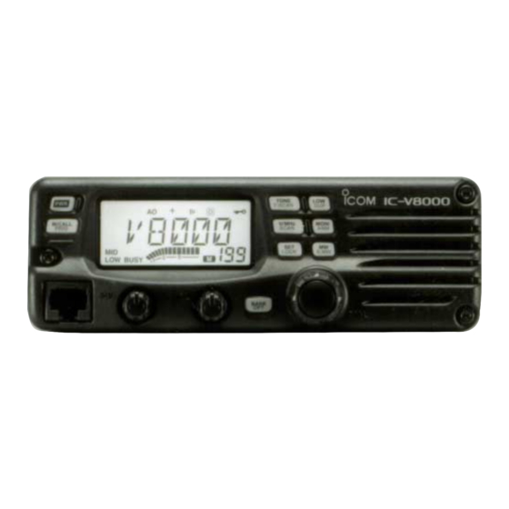
- Page 1 SERVICE MANUAL VHF FM TRANSCEIVER...
- Page 2 INTRODUCTION This service manual describes the latest service information for the IC-V8000 VHF FM TRANSCEIVER at the time of pub- lication. VERSION SYMBOL Asia C.S.America CSA-1 USA-2 U.S.A. USA-3 To upgrade quality, any electrical or mechanical parts and internal circuits are subject to change without notice or obligation.
-
Page 3: Table Of Contents
IC-V8000 ........ - Page 4 SECTION 1 SPECIFICATIONS ‘ ‘ GENERAL • Frequency coverage • Type of emission • Frequency stability • Tuning steps • Antnna connector • Power supply requirement (negative ground) • Number of memory channel • Call channel • Scanning mode • Current drain (approx.) •...
- Page 5 SECTION 2 • MAIN UNIT VCO circuit • LOGIC BOARD Speaker INSIDE VIEWS AF power amplifier (Q23: RD70HVF1) Reference oscillator (X1: CR-659) System clock (X1: CR-663) Reset IC (IC4: S-80942ANMP-DD6) 2 - 1 Antenna switching circuit (D12, D27: XB15A407, D19: XB15A308, D16: HVU131TRF) 2nd IF filter (FI1: CFWS450F,...
- Page 6 SECTION 3 DISASSEMBLY AND OPTION INSTRUCTIONS • REMOVING THE COVER 1 Unscrew 4 screws, MP10. 2 Remove the cover in the direction of the arrow. Cover • REMOVING THE FRONT PANEL 1 Unscrew 3 screws, MP9. 2 Unplug J6 to separate front panel and chassis. 3 Remove the front panel in the direction of the arrow.
-
Page 7: Receiver Circuits
SECTION 4 CIRCUIT DESCRIPTION RECEIVER CIRCUITS 4-1-1 ANTENNA SWITCHING CIRCUIT (MAIN UNIT) Received signals passed through the low-pass filter (L44, L47, L48, L51, C190, C197, C203, C208, C210, C217, C218). The filtered signals are applied to the 1/4 antenna switching circuit (D16, D19). The antenna swtiching circuit functions as a low-pass filter while transmitting. -
Page 8: Main Unit
The AF signals are applied to the AF power amplifier circuit (IC9, pin 1) to obtain the specified audio level. The amplified AF signals, output from pin 4, are applied to the internal speaker (CHASSIS UNIT; SP1) via the speaker jack (J6) when no plug is connected to the external speaker jack (J1). -
Page 9: Pll Circuits
PLL CIRCUITS 4-3-1 PLL CIRCUIT (MAIN AND LOGIC UNITS) A PLL circuit provides stable oscillation of the transmit fre- quency and receive 1st LO frequency. The PLL output com- pares the phase of the divided VCO frequency to the refer- ence frequency. -
Page 10: Hm-133V
PORT ALLOCATIONS 4-5-1 CPU (LOGIC UNIT: IC7) Port Description number name Input port for the weather alert signal DETO detection. RESET Input port for reset signal. Outputs reference oscillator for the CSHIFT CPU control signal. Outputs serial clock signal to the expander IC (MAIN unit;... - Page 11 4-5-2 D/A CONVERTOR IC (MAIN UNIT: IC5) Port Description number name Outputs transmit devetion control sig- nal. SQLATT Outputs attenuator control signal. • Outputs tunable bandpass filter con- trol signal while receiving. • Outputs TX power control signal while transmitting. Output tunable bandpass filter control 11, 23 T2, T3...
-
Page 12: Logic Board
SECTION 5 PARTS LIST [LOGIC BOARD] ORDER DESCRIPTION 1110002860 S.IC TA75S393F (TE85R) 1130004200 S.IC TC4S66F (TE85R) 1110005340 S.IC NJM12902V-TE1 1130009110 S.IC S-80942ANMP-DD6-T2 1130009680 S.IC HN58X2432TI 1130008090 S.IC BU4066BCFV-E1 1140010400 S.IC HD6433876B53H (FX-2509A) 1130007570 S.IC BU4094BCFV-E2 1530002690 S.TRANSISTOR 2SC4116-GR (TE85R) 1590000430 S.TRANSISTOR DTC144EUA T106 1590001650 S.TRANSISTOR XP4601 (TX) 1590000430 S.TRANSISTOR DTC144EUA T106 1590000660 S.TRANSISTOR DTC144TU T106... - Page 13 [LOGIC BOARD] ORDER DESCRIPTION 4030007090 S.CERAMIC C1608 CH 1H 470J-T-A 4030006860 S.CERAMIC C1608 JB 1H 102K-T-A 4030006900 S.CERAMIC C1608 JB 1H 103K-T-A 4030006860 S.CERAMIC C1608 JB 1H 102K-T-A 4030006860 S.CERAMIC C1608 JB 1H 102K-T-A 4030006860 S.CERAMIC C1608 JB 1H 102K-T-A 4030006860 S.CERAMIC C1608 JB 1H 102K-T-A 4030006860 S.CERAMIC...
- Page 14 [MAIN UNIT] ORDER DESCRIPTION 1750000710 S.VARICAP HVC350BTRF 1750000710 S.VARICAP HVC350BTRF 1710001060 DIODE XB15A407 1750000710 S.VARICAP HVC350BTRF 1790000980 S.DIODE MA742 (TX) 1750000550 S.DIODE 1SS355 TE-17 1710000870 S.DIODE HVU131TRF 1790000980 S.DIODE MA742 (TX) 1790001250 S.DIODE MA2S111-(TX) 1710001080 DIODE XB15A308 1730000520 ZENER RD20E B2 1790000700 DIODE DSA3A1 1790001520 S.ZENER...
- Page 15 [MAIN UNIT] ORDER DESCRIPTION R101 7030003720 S.RESISTOR ERJ3GEYJ 224 V (220 kΩ) R103 7030003680 S.RESISTOR ERJ3GEYJ 104 V (100 kΩ) R104 7030003740 S.RESISTOR ERJ3GEYJ 334 V (330 kΩ) R105 7030003680 S.RESISTOR ERJ3GEYJ 104 V (100 kΩ) R106 7030003560 S.RESISTOR ERJ3GEYJ 103 V (10 kΩ) R107 7030003710 S.RESISTOR ERJ3GEYJ 184 V (180 kΩ)
- Page 16 [MAIN UNIT] ORDER DESCRIPTION C105 4030006860 S.CERAMIC C1608 JB 1H 102K-T-A C106 4030006860 S.CERAMIC C1608 JB 1H 102K-T-A C108 4030006860 S.CERAMIC C1608 JB 1H 102K-T-A C109 4030006900 S.CERAMIC C1608 JB 1H 103K-T-A C111 4030009990 S.CERAMIC C1608 CH 1H 200J-T-A C112 4030007100 S.CERAMIC C1608 CH 1H 560J-T-A C113...
- Page 17 SECTION 6 MECHANICAL PARTS AND DISASSEMBLY 6-1 IC-V8000 [CHASSIS PARTS] REF. NO. ORDER NO. DESCRIPTION 6510004880 Connector MR-DSE-01 2710000720 Fan DF125020BH 8010018801 2509 Chassis-1 8030056880 2509 Fan holder 8110007670 2509 Cover 8810008660 Screw BT M3 x 8 NI-ZU (BT) 8810008660 Screw BT M3 x 8 NI-ZU (BT) 8810008660 Screw BT M3 x 8 NI-ZU (BT) 8810008030 Screw H M2.6 x 8...
- Page 18 MP14 (C) J1 (C) MP14 (C) MP4 (C) MP1 (C) MP14 (C) MP14 (C) MP12 (L) LOGIC unit MP2 (C) MP7 (L) MP3 (L) MF1 (C) MP2 (L) EP9 (L) MP12 (L) DS19 (L) MP4 (L) MP11 (C) MP1 (L) MP15 (C) MAIN unit MP6 (L)
- Page 19 6-2 HM-133V [MAIN UNIT] [CHASSIS PARTS] REF. NO. ORDER NO. REF. NO. ORDER NO. DESCRIPTION QTY. 8900010450 Cable OPC-153 8210018830 2539 Front panel Screw abbreviations 8210018890 2539 Front panel (A) 8210018910 2539 Front panel (B) 8210018840 2539 Rear panel 8930057380 2539 PTT button 8930057390 2539 LED lens 8930057570 SW rubber 8930057520 2539 Keyboard...
- Page 20 SECTION 7 SEMI-CONDUCTOR INFORMATION • TRANSISTOR AND FET’S 2SA1576 R 2SA1734 2SA1586 GR (Symbol: FR) (Symbol: LB) (Symbol: S0) 2SC3356 2SC4116 BL 2SC4116 GR (Symbol: R22) (Symbol: LL) (Symbol: LG) 2SC4406 4 2SC4684 (LB) 2SK1069 4 (Symbol: JT) (Symbol: 2-7B2A) (Symbol: FJ) 3SK272 DTA113 ZU...
- Page 21 SECTION 8 BOARD LAYOUTS 8-1 HM-133V • TOP VIEW DS11 • BOTTOM VIEW DS10 B5811B to Logic board J1 8 - 1...
- Page 22 8-2 LOGIC BOARD • TOP VIEW DS13 From External Microphone 8 - 2 DS10 DS11 DS14...
- Page 23 • BOTTOM VIEW R108 R110 B5801B to Main unit J1 to Main unit J2 to Optional unit OPV1 R111 OPV2 EXSTB OPT3 OPT2/CCS OPT1 R105 MICIN MICOUT R109 8 - 3 — OPT2/CCS — AFOUT DETO — — — — —...
- Page 24 8-3 MAIN UNIT • TOP VIEW C205 C195 R125 C118 to Logic board SP1 (SP) J5 (FAN) C177 C157 C207 to Chassis unit MF1 8 - 4 C147 C155 C150 R164 C235 C234 C137 C130 C238 C123 C116 C104 R108 R106 R150 C163...
- Page 25 • BOTTOM VIEW R131 R123 C183 C178 C158 C152 C145 R117 C160 C180 C138 R135 R136 R139 C224 R137 C232 R155 C101 R157 C134 C105 R130 C102 C140 C193 R152 C124 C133 C136 C240 C242 R154 R153 C128 C113 C111 R162 R161 C142...
- Page 26 SECTION 9 BLOCK DIAGRAM SHIFT IC1: LV2105V Q2: XP4601 LOOP (LOOP-SW) Q4: 2SC4116 D3: HVC376B X1: CR-659 Q10: 2SK1069 DC AMP IC4: TA31136FN IF DET-IC (2nd-MIX, IF-AMP, NOISE-AMP, FMDET, RSSI, SQLSW) CERAMIC FI1: CFWS450F MAIN UNIT IC3c: NJM12902V LOGIC BOARD IC2: TC4S66F D4: DAN222 IC3a: NJM12902V...
- Page 27 SECTION 10 VOLTAGE DIAGRAM 10-1 LOGIC BOARD MICIN EP1 MMZ1608Y102BT EP2 MMZ1608Y102BT EP3 MMZ1608Y102BT MICE EP4 MMZ1608Y102BT EP5 MMZ1608Y102BT From the Microphone EXTMIC EP6 MMZ1608Y102BT MICUD EP7 MMZ1608Y102BT EP8 MMZ1608Y102BT 3017-8821 0.001 0.001 0.001 0.001 0.001 NA8 091 M 47 P R101 R107 4.7 k...
- Page 28 1.5 M CONT.A CONT.D 10 k 0.0022 0.0027 CONT.B CONT.C 0.01 0.01 BU4066BCFV NJM12902V 27 k RMUT MODIN CTCSS CTCC CTCIN VOLIN AFON REMO MICUD MICUD SQLV SQLV DICK PDET DIUD CTCIN LVIN TEMP PDET 12 k CR-663 68 P PB0/AN0 AVSS TEST...
- Page 29 SECTION 10 VOLTAGE DIAGRAM 10-1 LOGIC BOARD MICIN EP1 MMZ1608Y102BT EP2 MMZ1608Y102BT EP3 MMZ1608Y102BT MICE EP4 MMZ1608Y102BT 330 k 100 k 0.01 EP5 MMZ1608Y102BT From the Microphone EXTMIC EP6 MMZ1608Y102BT 120 k MICUD EP7 MMZ1608Y102BT EP8 MMZ1608Y102BT TA75S393F 3017-8821 10 k MA8091 M 12 k DAN222...
- Page 30 10-2 MAIN UNIT SHIFT 0.001 0.33 10 k N TCCM20124A G473JCT 270 k TEMP 100 k XP4601 10 k C241 220 k 2.7 k CR-659 10 k 47 k 68 P 2SC4116 BL 470 k HVC376B 18 P 0.001 2.2 k 33 P LV2105V XOUT...
- Page 31 R151 0.15 C118 C122 C:13.0 V 0.001 EXC-ELDR25C EXC-EL DR25C 3225 3225 H C147 C150 C155 0.001 0.01 C126 C129 C142 0.001 0.01 0.001 LA-254 C109 60 nH 0.01 C135 RD70HVF1 100 P 7.5 nH C151 C159 C156 C228 56 P 56 P 100 P 39 P...
- Page 32 10-2 MAIN UNIT SHIFT 2SC4116 BL 0.001 T: 7.5 V R: 7.1 V 0.001 4.7 k T: 7.4 V R: 0 V 0.001 MA2S111 2SC4116 BL 22 k 0.001 0.33 T: 0 V T: 0 V 10 k R: 5.0 V 0.001 R: 0.7 V 2SK1069 4...
- Page 34 S-13815IZ-C1 1-1-32, Kamiminami, Hirano-ku, Osaka, 547-0003, Japan © 2002 Icom Inc.
Need help?
Do you have a question about the IC-V8000 and is the answer not in the manual?
Questions and answers