Table of Contents
Advertisement
Quick Links
Service Manual
List of JS-925 series Product
Name
Main Unit
POS Workstation
Option Unit Communication Board
USB HUB Board
Storage
Storage module Unit
Unit
Storage module Unit
JS-925 Series
POS Workstation
Model Number.
Remarks
12inch type POS Workstation without
JS-925WS-010
HDD
(Including HDD SATA Cable x 1)
15inch type POS Workstation without
JS-925WS-050
HDD
(Including HDD SATA Cable x 1)
JS-925WS-051
15inch type POS Workstation with HDD
China Model
15inch type POS Workstation without
JS-925WS-H50
HDD
(Including HDD SATA Cable x 1)
With AC Power Cable
China Model
15inch type POS Workstation without
HDD
JS-925WS-H52
(Including HDD SATA Cable x 1)
With Rear Display & AC Power Cable
JS-925CB-010
IO extension Board
China Model
JS-925CB-H10
IO extension Board
JS-925HU-010
USB HUB Board
2.5 HDD module
JS-925HD-010
(Including HDD SATA Cable x 1)
JS-925SS-010
2.5 SSD module
1
ORDER NO. MSBU0912001C0
V.1.14 (2010.11.5)
© 2010 Panasonic System Networks Co., Ltd.
All right reserved. Unauthorized copying and
distribution is a violation of law.
G20
Advertisement
Table of Contents

Related Manuals for Panasonic JS-925WS-010


Summary of Contents for Panasonic JS-925WS-010
- Page 1 2.5 HDD module Storage module Unit JS-925HD-010 Unit (Including HDD SATA Cable x 1) Storage module Unit JS-925SS-010 2.5 SSD module © 2010 Panasonic System Networks Co., Ltd. All right reserved. Unauthorized copying and distribution is a violation of law.
- Page 2 List of Peripheral Product MSR Unit JS-950MG-010 Magnetic stripe reader module ID module Dallas Key Reader Unit JS-950DP-010 Dallas KEY Reader module Unit Fingerprint Sensor Unit JS-950FS-010 Fingerprint Sensor module Rear Display Rear Display Unit JS-790RD-010 Rear Display module 2line Block JS-950KT-A25 AC cord kit...
- Page 3 WARNING This service information is designed for experienced repair technicians only and is not designed for use by the general public. It does not contain warnings or cautions to advise non-technical should be potential dangers in attempting to service a product.
- Page 4 Version List Version Date Page Modification 1.01 2009.12.24 Added HDD Manufacturer’s Parts No. 1.02 2010.1.12 Deleted 5. Flash and Updating BIOS. Updated Replacement Parts List. Added Information of Safety Standard and EMI & immunity 1.03 2010.1.21 Cover Added (Including HDD SATA Cable x 1). Added HDD Option.
-
Page 5: Table Of Contents
CONTENTS 1. Overview ..........................................1 1.1. General ..........................................1 1.2. Specifications ....................................... 2 1.3. Outside drawing ......................................5 1.4. I/O Connectors layout ....................................6 1.5. Pin Assignment ......................................8 1.6. Jumpers ........................................10 2. Description of Operation ....................................10 2.1. Block Diagram ......................................10 2.2. - Page 6 6.1.2. Replacement Parts List ................................149 6.2. JS-925WS-050/051 LCD Unit................................. 151 6.2.1. Disassembly Drawing ..................................151 6.2.2. Replacement Parts List ................................163 6.3. JS-925WS-010 LCD Unit ................................... 164 6.3.1. Disassembly Drawing ..................................164 6.3.2. Replacement Parts List ................................176 7. Trouble Shooting ......................................177 Appendix [JS-925CB-010 Installation Instruction] ..........................
-
Page 7: Overview
1. Overview 1.1. General JS-925WS was designed for Mid-range. Main Body was transplanted from JS-790WS. LCD Unit was transplanted from JS-950WS. Mother Board was re-designed with new CPU Intel® ATOM N270 1.6GHz. For other detail specifications, see the following Specifications. -
Page 8: Specifications
1.2. Specifications [ Common Specifications ] Environmental condition Item Specification Operating Temperature +5°C – +40°C Operating Humidity 15% RH – 85% RH (no dew) Strage Temperature -30°C – +60°C Strage Humidity 10%RH – 90%RH [ POS Workstation: JS-925WS-xxx ] Item Specification Type... - Page 9 Item Specification Type 5-wire resistive Interface Serial Touch Panel Life 30 Million touches or more Surface Non-glare surface treatment 4 Ports 9pin D-SUB male Serial - Note: 2 ports are Powered. 1 Port 15pin D-SUB female Video - Note: The Dual Display function is supported. 1 Port RJ-45 2 USB Ports: IO panel I/O ports...
- Page 10 Item Specification JS-925CB-010 / JS-925CB-H10 Expansion IO I/F + Speaker I/F : Expansion I/F - Line-OUT 1port - USB 2.0 2ports Communication - Din type Drawer 1port (Same as JS-950WS) board Note: The power of +12V, 1A is required to drive DIN type cash drawer Carton Box Size: 500mm x 400mm x 270mm Mass: NET: 1.452Kg GROSS:2.8Kg...
-
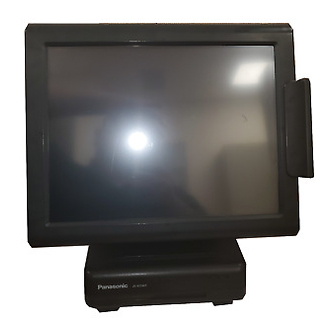
Page 11: Outside Drawing
1.3. Outside drawing 12” Touch Screen 15” Touch Screen... -
Page 12: I/O Connectors Layout
1.4. I/O Connectors layout (1) Bottom IO Connector layout Speaker LINE-OUT USB#3,#4 DIN Drawer#3 (Option) (Option) (Option) (Option) COM4 COM3 ○○○○ ○○○○ ○○○○○ ○○○○○ ○○○○○ ○○○○ ○○○○ ○○○○ ○○○○○ ○○○○○ ○○○○○ COM2 COM1 USB#2 RJ Drawer#1, #2 Ethernet (Powered) (Powered) USB#1 (2) Front IO Connector layout SW &... - Page 13 (3) USB Port Positions USB#6:standard For Display unit USB I/F USB#7:Reserved (For future use) USB#8:standard USB#5:standard (Inside of rear cover) (Inside of front cover) USB#1#2:standard USB#3#4:Option (IO Panel) (IO Panel)
-
Page 14: Pin Assignment
1.5. Pin Assignment (1) Ethernet : 8 pin Modular (RJ45) PIN# Signal PIN# Signal (2) USB : USB Connector PIN# Signal PIN# Signal Data + Data - (3) Powered COM port COM1, COM2 : 9 pin D-SUB Male PIN# Signal PIN# Signal RI (default) / +5V / +12V... - Page 15 (6) Cash Drawer (DIN type): 6 pin DIN Female PIN# Signal PIN# Signal Drawer #3 Open Drawer Type Drawer #3 Status (7) Cash Drawer (RJ type) : 6 pin Modular (RJ11) PIN# Signal PIN# Signal +24V CD #1 Open CD # 2 Open CD # 1 and #2 Status CD # 1 and #2 Status return NOTE:...
-
Page 16: Jumpers
1.6. Jumpers 1. JP271 and JP272 Powered COM Setting No. 9 pin of COM1 & 2 can be changed as follows. Jumper Setting JP271 for COM1 JP272 formCOM2 1-2 Short 3-4 Short RI (Default) RI (Default) 5-6 Short +12V +12V 2. - Page 17 3. JP371 Battery Charging Voltage Setting Jumper Setting 1-2 Short For Current Battery (40ohm, Default) 2-3 Short For the future Battery...
-
Page 18: Description Of Operation
2. Description of Operation 2.1. Block Diagram DISPLAY OPTION CUSTOMER DISPLAY MSR JIS-1,2 etc Rear Display Kit JS-790RD-010 TP-CNT board Touch Panel OPTION (Higgstec) VFD-2 Lines CU20029-T303C (Noritake) 15"INV LCD Power LED LAN LED HDD LED Green/Red Green G150XG03V1 (AUO) Green Power 12"INV... -
Page 19: Description Of Pcb Circuit
2.2. Description of PCB Circuit 2.2.1 Main PCB Ref. No. Parts No. Parts Name & Description Pecs U051 YJ30-123722 ASIC AU80586GE025D SLB73 C0 FC-BGA8 437P Chip Set / Memory Controller U081 YJ30-123723 ASIC QG82945GSE SLB2R A3 FC-BGA3 998P North Bridge Video Controller (direct connection to Video I/F) HDD Controller Drawer Controller (Standard I/O Port) - Page 20 Ref. No. Parts No. Parts Name & Description Pecs U362 YJ32-974660S IC ADM1815-R23ARTZ-RL SOT-23 U372,U373 YJ32-971543S IC MIC841HYC5 SC70-5 (LF) Q161 YJ35-950028S TR DUAL FFB3904 SC70-6 FAIRCHILD Q162,Q163,Q211, Q214,Q216,Q222, Q223,Q241,Q242, Q243,Q244,Q245, Q246,Q247,Q248, Q302,Q303,Q305, Q308,Q331,Q333, Q334,Q336,Q337, Q338,Q351,Q352, YJ35-339001S MOSFET TR 2N7002 SOT-23 FAIRCHILD Q353,Q354,Q355, Q356,Q357,Q358, Q359,Q362,Q367,...
- Page 21 +24V for Cash Drawer generation area +5V generation area U271 U272 Y201 Q371 U202 Q217 Q311 U313 +1.8V for Memory generation area U321 +3.3V U051 generation area U081 U341 U332 Y251 U252 U191 U251 Q332 U141 U261 U281 +1.5V for Chipset Core generation area...
- Page 22 +0.9V for Memory U322 Terminator generation area U291 U292 U214 +1.5V generation area...
-
Page 23: Touch Panel Pcb
2.2.2 Touch Panel PCB Ref. No. Parts No. Parts Name & Description Pcs/set YJ30-123189 Controller TP Controller ASIC MCU 16K F/W:1.08.D2-AI MLP-28 U14,U15,U24 YJ35-390351S TR FET P-CHANNEL SI1555DL-T1-E3 SOT-363 YJ30-526683S EEPROM 4K AF93BC66-SI SOIC8 APLUSFLASH YJ32-300015S Transceiver RS-232C Transceiver IC RS-232 TRANSCEIVER SO16 SP202EEN YJ32-974712S Regulator Regulator for RS-232C... -
Page 24: I/O Board
2.2.3 I/O Board Ref. No. Parts No. Parts Name & Description Pcs/set +5V Regulator for Audio Codec (U2) (+5V is created from YJ32-960258S Regulator IC REGUALTOR MC78M05CDTRKG DPAK-3 +12V) YJ30-123256S Audio Codec Audio Codec (Sound Output) ASIC ALC662-GR LQFP48 REALTEK YJ38-950121S IC TVS D ARRAY NUP4102XV6T1G SOT563 YJ32-970523S... - Page 25 Audio AMP area...
-
Page 26: Usb Hub Pcb
2.2.4 USB HUB PCB Ref. Parts No. Parts Name & Description YJ38-950088S D ARRAY DVIULC6-4SC6 SOT23-6L ST YJ30-123603S Controller HUB Controller IC USB HUB CONTROLLER QFN36 USB2512-AEZG YJ32-974712S Regulator Regulator for HUB Controller (U1) (?V is created from +5V) LDO REGULATOR ad 3A GS1085LDF TO-252 YJ44-345600S Crystal Clock for HUB Controller... -
Page 28: Test Program (Ediag)
3. Test Program (eDiag) 3.1. Initiation method of test program Before executing e-Diag, please make sure the setting of ATA/IDE configuration is “Compatible Mode”. If not, please enter the BIOS Advanced Page and change the setting of ATA/IDE configuration from “Enhanced Mode”... - Page 29 at “Diag. 3-1 Workflow”, “Table 3-1 Option Feature List and Operation Method” and “Diag. 3-7 Diagnostic program (Workflow) Initiation method of DISK version 925DISK Start from MS-DOS prompt The power supply of JS-925 is turned on. If the prompt of MS-DOS is displayed, it is input as " 925DISK.EXE ".
-
Page 30: Diagnostic Test Mode
3.2. Diagnostic Test Mode 3.2.1. Diagnostic Test Mode Selection The Diagnostic test mode can be selected in Diagnostic test mode selection page of the BIOS Setup Manager. Reference the following Figure 4-1. Figure 4-1 Diagnostic Test Mode Selection 3.2.2. Diagnostic Test Mode Description. Interactive Administration Mode Description: If user selected the Interactive Administration mode (restricted by password) in Diagnostic test mode selection page, user can select to run a test item from all test items individually after inputting password as the... - Page 31 e-Diag Test Mode Selection---V1.10 Password Set **** Set and press ENTER key ENTER Interactive User Mode Description If user selected the Interactive User Mode in Diagnostic test mode selection page, user can select to run limited test items. Automatic Mode Description. If user selected the Automatic mode in Diagnostic test mode selection page, test items runs automatically.
-
Page 32: Operation Mode
3.3. Operation mode This test program 4 kinds of mode, “Interactive-Administrator mode” “Interactive-User mode” “Automatic mode” "Heat run mode". (However, ROM version i.e. 925ROM.BIN has 4 modes. DISK version i.e. 925DISK.EXE has all 4 modes.) 3.3.1. Interactive-Administrator mode It uses it in this mode usually. The worker can operates it with a touch panel or a keyboard. NOTE: * mark in front of each test items means that this item was selected for Heat Run Test. -
Page 33: Interactive-User Mode
3.3.2. Interactive-User mode The worker can operates it with a touch panel or a keyboard. Interactive-User mode does not have “Heat Run Test”, so [*] mark can not be shown in the following page. NOTE: V9.99 means version number. Main menu screen in the Interactive User mode (DISK version) ***** Interactive User Mode---V1.10 *** 0 : EXIT. -
Page 34: Heat Run Mode
3.3.3. Heat run mode It is possible to test automatically repeating only the targeted item of the test items. (However, there are a test item for the heat run and an item of the uncorrespondence. ) The test frequency and test result are displayed in LCD at any time. The test frequency of the heat run test is assumed to be infinite times. - Page 35 3.3.3.3 Result of heat run test display The result of the heat run test is displayed on the LCD screen. The error frequency of each test item and the test frequency as the whole are displayed. ***** Heat Run Test. ***** TEST COUNT=1 (ERROR TIMES) Random Access Memory Test...
-
Page 36: Diagnosis Item
3.4. Diagnosis item 3.4.1. Random Access Memory Test. Screen of LCD (Processing) ***** Random Access Memory Test . ***** RAM write/Read Test. 16384 KB OK. RAM Address is up to 00FFFFFFH RAM Refresh Test. 16384 KB OK. RAM Address is up to 00FFFFFFH F1=STOP / CONTINUE F2=STOP / MENU TEST=RUN F1=STOP/ CONTINUE F2=STOP / MENU... -
Page 37: Hard Disk Test
3.4.2. Hard Disk Test. Screen of LCD ***** HDD Test. ***** 0 : Return to MAIN MENU. 1 : HDD 1 Test. 2 : HDD 2 Test Select and press ENTER key : 0_ ENTER 1) LED for HDD blinks in green is confirmed while testing Read Screen of LCD (Processing) ***** HDD Test.***** HDD CONTROLLER Test... -
Page 38: Video Test
***** HDD Test.***** HDD Card CONTROLLER Test OK HDD Card SEEK Test OK HDD Card Read Test OK Reading : Cylinder =374 Head =7 Sector =16 Sector count =1 Test done. Press any key. EXIT 3.4.3. Video Test Screen of LCD ***** Video Test. - Page 39 ***** Video White Screen Test.***** ENTER 1 (OK) or 2 (NG) 1(OK) 2(NG) 2) All black screen It is confirmed that there is neither dot omission nor a misregistration. If it is OK, press [1 (OK)] button or press [1] key in keyboard If it is NG, press [2 (NG)] button or press [2] key in keyboard.
- Page 40 (all red) A few seconds later ***** Video Red Screen Test.***** ENTER 1 (OK) or 2 (NG) 1(OK) 2(NG) 4) All green display It is confirmed that there is neither dot omission nor a misregistration. If it is OK, press [1 (OK)] button or press [1] key in keyboard If it is NG, press [2 (NG)] button or press [2] key in keyboard.
- Page 41 ***** Video Green Screen Test.***** ENTER 1 (OK) or 2 (NG) 1(OK) 2(NG) 5) All blue test It is confirmed that there is neither dot omission nor a misregistration. If it is OK, press [1 (OK)] button or press [1] key in keyboard If it is NG, press [2 (NG)] button or press [2] key in keyboard.
-
Page 42: Battery Test
3.4.3.2. VRAM TEST While this test is executing, the screen maybe displayed garbage. However beep sounds let you executing the VRAM test normally. Screen of LCD ***** Video Test. ***** ***** VRAM TEST ***** VRAM Size : ** KB Read/Write test : ********H Test done. - Page 43 The AC Power is turned off by user manually within 10 seconds. (The power supply keeps from the battery.) And then, user needs to turn ON again manually. ******* Status Check Test. ***** Please Turn Off AC Power, re-plug in again when you hear beep sounds Press [F1] key to exit.
-
Page 44: Serial Port Test
3.4.4.2. Power Fail Test ***** Power Fail Test. ***** Please Turn Off AC Power, re-plug in again when you hear beep sounds Press [F1] key to exit. Test result is . F1=STOP/CONTINUE F2=STOP / MENU The AC Power is turned off by user manually within 10 seconds. (The power supply keeps from the battery.) And then user needs to turn ON again manually. - Page 45 ***** Serial Port Test.***** 0 : Return to MAIN MENU 1 : Test COM1 2 : Test COM2 3 : Test COM3 4 : Test COM4 Select and press ENTER key : 0_ ENTER Screen of LCD ***** Serial Port Test.***** Test COM* (I/O Address 0****) RS232C Controller Register R/W Test OK INTERNAL LOOPBACK Test OK...
-
Page 46: Customer Display Test
3.4.6. Customer Display Test Screen of LCD ***** Customer Display Test.***** 0 : Return to MAIN MENU 1 : 2Line VFD Test Select and press ENTER key : 0_ ENTER The screen after each test is executed is as follows. 3.4.6.1. -
Page 47: System Information Test
Korean character (ten characters) code: A4A1-A4AA Simplified Chinese character (ten characters) code: A4A1-A4AA Traditional character (ten characters) code: B0A1-B0AA Screen of LCD (Processing) ***** 2 Line VFD Test. ***** ENTER 1 (OK) or 2 (NG) 1(OK) 2(NG) OK or NG is selected, by touch panel or by keyboard. Screen of LCD ***** 2 Line VFD Test. - Page 48 ***** System Information Test. ***** 0 : Return to MAIN MENU. 1 : Read System Information 2 : View Smart Value 3 : Event Log Select and press ENTER key : 0_ ENTER 3.4.7.1. Read System Information Read and display the following data in DMI/SMBIOS. Manufacture Product Number Version...
- Page 49 3.4.7.2. View Smart Valued SMART value of HDD ***** System Information Test. ***** AttID Name Supposition Value 0009H “Power On Hours” 9999Hours 000CH “Power Cycle Count” 9999 Test done. Press any key EXIT Light Brown 3.4.7.3. Event Log NOTE: if the mode is “Interactive User”, “2: Clear Log” is NOT displayed. Screen of LCD ***** Event Log ..***** 0: Return to MAIN MENU...
- Page 50 Event Description Event Log format (8 byte) Offset content Remark Event log type length These fields contain the BCD representation of the date and time (as read from CMOS) of the most recent occurrence of the event. The information is present in year, month, day, hour, minute, second order.
-
Page 51: Touch Panel Test
***** Event Log . ***** Test done. Press any key EXIT Light Brown 3.4.8. Touch Panel Test Screen of LCD ***** Touch Panel Test.***** 0: Return to MAIN MENU 1: CALIBRATION. TOUCH TEST Select and press ENTER key : 0 ENTER... - Page 52 3.4.8.1. Calibration The same calibration as the ordinary mode. The calibration of T/P of EETI is as following: The Four cross marked the press point will be displayed sequencly from low-left ,low-right, up-right and up-left while you pressed the “+” cross mark ,reference the following diagram. Note) When application is run on Windows, it is recommended to calibrate touch panel by Windows Tool.
- Page 53 Please press 2 points...
- Page 54 When calibration ends normally, the following screen is displayed. ***** Touch Panel Test ***** CALIBRATION Test done. Press any key. EXIT Light Brown 3.4.8.2. Touch Test Push the “2” and “ENTER”, then TOUCH TEST starts. Screen of LCD ***** Touch Panel Test.***** 0: Return to MAIN MENU 1: CALIBRATION.
-
Page 55: Drawer Test
Blue colored square mark. Press to exit test. It changes to the following screens when (21, 16) are pressed. ***** Touch Panel Test. ***** TOUCH TEST ENTER 1 (OK) or 2 (NG) 1(OK) 2(NG) OK or NG is selected, and it returns to Touch Panel Test. Screen of LCD ***** Touch Panel Test ***** TOUCH TEST... - Page 56 Screen of LCD ***** Drawer Test.***** 0 : Return to MAIN MENU 1 : DRAWER1 2 : DRAWER2 2 : DRAWER3 Select and press ENTER key : 0_ ENTER Light Brown 3.4.9.1. DRAWER 1 Screen of LCD (If already opened) ***** Drawer Test ***** DRAWER #1 and/or #2 Already open Test done.
- Page 57 ***** Drawer Test ***** Drawer 1 is open ? Test done. Press any key. EXIT Light Brown 3.4.9.2. DRAWER 2 This test item is the same as DRWER 2. 3.4.9.3. DRAWER 3 This test item is the same as DRWER 3.
-
Page 58: Ether Test
3.4.10. Ether Test Preprocessing Acquisition of base address Initialization of PCI Configuration(bus master enable) Acquisition of MAC Address 3.4.10.1. Self Test Check the LAN chip internally, and whether network cable is connected or not. Diagnostic program can detect network communication speed if connected to HUB. Screen of LCD ***** Ether Test.***** ***** Self Test *****... - Page 59 ***** USB Test. ***** 0 : Return to MAIN MENU 1 : USB Interface Test. Select and press ENTER key : 0_ Enter Screen of LCD ***** USB Test. ***** USB Interface Test PORT 1 Low speed device connected USB Interface Test PORT 2 Low speed device connected USB Interface Test PORT 3 Low speed device connected USB Interface Test PORT 4 Low speed device connected USB Interface Test PORT 5 Low speed device connected...
-
Page 60: Audio Test
3.4.12. AUDIO TEST Screen of LCD ***** Audio Test. ***** 0 : Return to MAIN MENU 1 : Speaker(Earphone) TEST 2 : BUZZER TEST Select and press ENTER key : 0_ Enter 3.4.12.1. Speaker(Earphone) Test Diagnostic program can play a short sound one time. Screen of LCD ***** Audio Test. - Page 61 3.4.12.2. Buzzer TEST Diagnostic program can make sol-fa sounds. ***** Buzzer Test. ***** BUZZER 1(OK) 2(NG) After finishing the test. ***** Buzzer Test. ***** BUZZER ENTER 1 (OK) or 2 (NG) 1(OK) 2(NG) OK or NG is selected, by touch panel or by keyboard. Screen of LCD ***** Buzzer Test.***** BUZZER...
-
Page 62: Backlight Test
3.4.13. Backlight TEST ***** Backlight Test. ***** 0 : Return to MAIN MENU. 1 : 1st Display Test. Select and press ENTER key : 0_ ENTER Diagnostic Program turns off and on back light 5 times (interval time is 0.5 seconds). And then show the following screen. -
Page 63: I-Button Test
3.4.14. i-Button TEST In technical point of View, diagnostic program cannot distinguish “i-Button”. It can detect only “Low Speed Device” or “High Speed Device”. Whether “Low” or “High” depends on the specific device, so please refer and confirm the specification of “i-Button”. 3.4.15. -
Page 64: Message List
3.5. Message list Explanation of messages when inspecting it is done as follows. 3.5.1. Random Access Memory Test NO. Message Cause Error ! RAM Read/Write Test failed. Write/Read error of RAM Address XXXXXXXXH Read data=XX Write data=XX Error ! RAM Refresh failed. After the fixed time, the value of RAM is not Address XXXXXXXXH maintained. -
Page 65: Audio Test
Modem Status : XX Expected : XX Loopback Test among DSR of the modem status, CTS, RI, and RLSD is one. RS232C Data Real loopback interrupt request failed The time-out was done without generating the LINE STATUS : XX interrupt of the cereal in External Loopback Test. RS232C Serial port data real loopback Test failed The line change of state interrupt went up in Line status : XX... -
Page 66: Backlight Test
3.5.13. BackLight Test. Only OK/NG... -
Page 67: Pcb
4. PCB 4.1. Main PCB 4.1.1. Schematic Diagram p49_MAIN_schemati c.pdf +40 pages... -
Page 68: Parts Location
4.1.2. Parts Location p50-1_MAIN_01_PC B.pdf +1 page (Total +41 pages) p50-2_MAIN_PCB_0 2.pdf +1 page (Total +42 pages) -
Page 70: Replacement Parts List
4.1.3. Replacement Parts List Note: When ordering replacement parts, indicate Part No .and Name of Parts. RTL marking Remarks means “Repairable PCB Assembly” “Retention Time Limited”. Pcs/ Ref. No. Parts No. Parts Name & Description Remarks U051 YJ30-123722 ASIC AU80586GE025D SLB73 C0 FC-BGA8 437P U081 YJ30-123723 ASIC QG82945GSE SLB2R A3 FC-BGA3 998P... - Page 71 Q162,Q163,Q211, Q214,Q216,Q222, Q223,Q241,Q242, Q243,Q244,Q245, Q246,Q247,Q248, Q302,Q303,Q305, Q308,Q331,Q333, Q334,Q336,Q337, TRANSISTOR Q338,Q351,Q352, 50 PCS PACK YJ35-339001S MOSFET TR 2N7002 SOT-23 FAIRCHILD Q353,Q354,Q355, Existing parts of Q356,Q357,Q358, 950WS Q359,Q362,Q367, Q376,Q377,Q2611, Q2612,Q2613,Q2614, Q3010,Q3012,Q3013, Q3014,Q3015,Q3510, Q3710,Q3711,Q3511, Q3512 TRANSISTOR Q164 YJ35-220018S PNP TR MMBT3906LT1G SOT23 ON-SEMI L/F 100 PCS PACK...
- Page 72 Pcs/ Ref. No. Parts No. Parts Name & Description Remarks TRANSISTOR 20 Q215,Q332,Q341 YJ35-390614S TR FET DULE N CHANNEL FDS6982AS SO8 PCS PACK TRANSISTOR 20 Q217 YJ35-390502S TR N-CHANNEL MOSFET FDS8896 SO-8 PCS PACK TRANSISTOR Q221 YJ35-339215S TR FET P-CHANNEL APM2301AAC SOT-23 100 PCS PACK Q301,Q306,Q309, TRANSISTOR 50...
- Page 73 Pcs/ Ref. No. Parts No. Parts Name & Description Remarks CONNECTOR 10 J361 YJ53-012489S CONN BOX HEADER SMD1*14 P1.25MM TIN PCS PACK CONNECTOR J371 YJ53-193997S CONN W-B DIP2 53258-0229 TIN L/F 100 PCS PACK JP141(1&2), CONNECTOR JP371(1&2), 100 PCS PACK YJ53-916037S JUMPER 2*1 P=2.54MM OPEN 6MM BLACK G/F JP271(3&4),...
-
Page 74: Switch & Led Pcb
4.2. Switch & LED PCB 4.2.1. Schematic Diagram 93_SW LED_schematic.pdf +3 pages... -
Page 75: Parts Location
4.2.2. Parts Location p95_SW LED_PCB.pdf +1 page (Total +4 pages) -
Page 76: Replacement Parts List
4.2.3. Replacement Parts List Note: When ordering replacement parts, indicate Part No .and Name of Parts. RTL marking Remarks means “Repairable PCB Assembly” “Retention Time Limited”. Pcs/ Ref. No. Parts No. Parts Name & Description Remarks TRANSISTOR 50 PCS PACK YJ35-110034S NPN TR MMBT3904 SOT23 Existing parts of... -
Page 77: Touch Panel Pcb
4.3. Touch Panel PCB 4.3.1. Schematic Diagram p99_TOUCH PANEL_scematic.pdf... -
Page 78: Parts Location
4.3.2. Parts Location p100_TOUCH PANEL PCB.pdf... -
Page 79: Replacement Parts List
4.3.3. Replacement Parts List Note: When ordering replacement parts, indicate Part No .and Name of Parts. RTL marking Remarks means “Repairable PCB Assembly” “Retention Time Limited”. Pcs/ Ref. No. Parts No. Parts Name & Description Remarks YJ30-123189 ASIC MCU 16K F/W:1.08.D2-AI MLP-28 TRANSISTOR U14,U15,U24 YJ35-390351S... -
Page 80: Js-925Cb-010 Optional I/O Pcb
4.4. JS-925CB-010 Optional I/O PCB 4.4.1. Schematic Diagram p102_IO_schematic. +6 pages... -
Page 81: Parts Location
4.4.2. Parts Location p103_IO_PCB.pdf +1page (Total +7 pages) -
Page 83: Replacement Parts List
4.4.3. Replacement Parts List Note: When ordering replacement parts, indicate Part No .and Name of Parts. RTL marking Remarks means “Repairable PCB Assembly” “Retention Time Limited”. Pcs/ Ref. No. Parts No. Parts Name & Description Remarks YJ32-960258S IC REGUALTOR MC78M05CDTRKG DPAK-3 IC 50 PCS PACK YJ30-123256S ASIC ALC662-GR LQFP48 REALTEK... -
Page 84: Js-925Hu-010 Usb Hub Pcb
4.5. JS-925HU-010 USB HUB PCB 4.5.1. Schematic Diagram p110_USB_schemati c.pdf +4 pages... -
Page 85: Parts Location
4.5.2. Parts Location p111_USB_PCB.pdf... -
Page 87: Replacement Parts List
4.5.3. Replacement Parts List Note: When ordering replacement parts, indicate Part No .and Name of Parts. RTL marking Remarks means “Repairable PCB Assembly” “Retention Time Limited”. Pcs/ Ref. No. Parts No. Parts Name & Description Remarks DIODE ARRAY YJ38-950088S D ARRAY DVIULC6-4SC6 SOT23-6L ST 20 PCS PACK IC 100 PCS YJ30-123603S... -
Page 88: Cable
5. Cable Cable list Pcs/ Ref. No. Parts No. Parts Name & Description Remarks CABLE ASSY, switch LED/B to M/B 190MM CABLE ASSY, PSU TO MB 165MM CABLE ASSY, HDD(SIGNAL & POWER) 180MM COM Cable D-SUB9_M to 10F 65mm RoHS CABLE ASSY, AC-in cable 180MM CABLE ASSY, TP &... - Page 89 p117_cable_01.pdf p117_cable_02.pdf p117_cable_03.pdf p117_cable_04.pdf p117_cable_05.pdf p117_cable_06.pdf p117_cable_07.pdf p117_cable_08.pdf...
-
Page 90: Body Block
6. Body Block 6.1. JS-925WS-xxx Main Unit. 6.1.1. Disassembly Drawing 1. Removal LCD Unit 1.1. Remove 2 screws. 1.2. Remove Cable Cover. - Page 91 1.3. Disconnect Cables. 1.4. Remove 4 screws. 1.5. Lift up LCD Unit. 1.6 Remove 2 screws.
- Page 92 1.7. Remove LCD unit Connect Earth Cable such as the following picture in case of assembly.
- Page 93 2. Removal Rear Cover. 2.1. Loosen screw. 2.2. Lift up Rear Cover. 2.3. Open Rear Cover.
- Page 95 3. Removal Front PCB and Power Supply. 3.1. Remove the 2 screws. 3.2. Remove Front Cover 3.3. Remove Front Case...
- Page 96 3.4. Disconnect the cable. 3.5. Remove the 2 screws. 3.6 Remove Front PCB.
- Page 97 3.7. Disconnect the cable.
- Page 98 3.8. Remove the 2 screws. 3.9. Remove Power Supply Shield.
- Page 99 Check some points as shown in the following pictures in case of assembly.
- Page 101 3.10. Disconnect the cable.
- Page 102 3.11. Disconnect the cable. 3.12. Remove the 4 screws. 3.13. Pinch the head of pillars by pliers, then lift up Power Supply unit for removal Power Supply unit.
- Page 104 4. Removal Battery (Option = Spare Parts, Ni-CD: N4HKLNB00007, Ni-MH: TBD) , HDD, Communication Board and Main PCB. 4.1. Disconnect the cable.
- Page 105 4.2. Remove the 2 screws. 4.3. Remove Battery cover and Battery. Battery (Option=Spare Parts, Ni-CD: N4HKLNB00007, Ni-MH: TBD)
- Page 106 4.4. Remove the 2 screws. 4.5. Remove PCB Shield such as shown in the following picture.
- Page 107 4.5. Disconnect the cable. 4.6. Disconnect the cable.
- Page 108 4.7. Remove the 4 screws. 4.8. Remove HDD.
- Page 109 4.9. Remove the 3 screws. 4.10. Disconnect the cable. 4.11. Remove Communication Board.
- Page 110 JS-925CB-010 4.12. Remove the 11 screws. 4.13. Disconnect the cables.
- Page 111 4.14. Remove Main PCB. 4.15. Remove DIMM.
- Page 112 Side A Side B...
- Page 113 Mount the Main PCB with fitting the holes and bosses such as shown in the following pictures in case of assembly.
- Page 114 5. Removal Base Frame. 5.1. Remove the 2 screws.
- Page 115 5.2. Remove the 2 screws. 5.3. Remove the base frame.
- Page 116 5.4. Remove the 2 screws. 5.5. Remove I/O Panel.
- Page 117 5.6. Remove the 4 hex screws. 5.7. Remove the 2 connector cables.
- Page 119 5.8. Remove the 3 screws. 5.9. Remove the 2 pillars.
- Page 120 5.10. Remove 5 screws.
-
Page 121: Replacement Parts List
6.1.2. Replacement Parts List Note: When ordering replacement parts, indicate Part No .and Name of Parts. RTL marking Remarks means “Repairable PCB Assembly” “Retention Time Limited”. Pcs/ Ref. No. Parts No. Parts Name & Description Remarks The same as Hinge Cover “3DA002298CAA”... - Page 122 Pcs/ Ref. No. Parts No. Parts Name & Description Remarks The same as YJ57-102865 Lower Case Assy 3VA002201DAA of JS-790WS YJ51-102477 Cable tie holder of KITAGAWA KB-07 YJ51-102469 SW Blind Sheet YJ51-102461 RUBBER FOOT YJ51-102692 Switch CAP YJ48-950380 SO-HEX,UNC#4-40*5*4.5+5.5,CU,NI,PATCH YJ51-103016 HDD Cable Connector Holder M3*0.5*6,PH,RND,ST,NI,SW+W M3*0.5*6,PH,BND,ST,ZB...
-
Page 123: Js-925Ws-050/051 Lcd Unit
6.2. JS-925WS-050/051 LCD Unit. 6.2.1. Disassembly Drawing 1. Remove the 2 screws. 2. Remove LCD Cable Cover A and B. - Page 124 3. Remove the 2 screws. 4. Disconnect USB Hub Board (JS-925HU-010). JS-925HU-010...
- Page 125 5. Remove the 2 screws. 6. Remove the 4 screws. 7. Remove Hinge.
- Page 126 8. Loosen the 4 screws until sounds clicky. 9. Remove the 4 screws.
- Page 127 10. Open Display Front Cover. 11. Remove the 4 screws.
- Page 128 12. Lift up TP+LCD. Then, disconnect Backlight Cables. 13. Disconnect LCD cable.
- Page 129 14. Disconnect Touch Panel Cable. 15. Open TP+LCD.
- Page 130 16. Remove the 4 screws. 17. Remove the tape.
- Page 131 18. Separate Touch Panel and LCD.
- Page 132 19. Remove the 3 screws. And remove Inverter Board.
- Page 133 20. Remove the 2 screws. And remove Touch Panel Control Board. 21. Remove the Cables.
-
Page 135: Replacement Parts List
6.2.2. Replacement Parts List Note: When ordering replacement parts, indicate Part No .and Name of Parts. RTL marking Remarks means “Repairable PCB Assembly” “Retention Time Limited”. Ref. No. Parts No. Parts Name & Description Pcs/set Remarks YJ51-102474 Hinge Cover YJ51-102475 Hinge USB Cable Cover YJ50-006390 15LCD Hinge... -
Page 136: Js-925Ws-010 Lcd Unit
6.3. JS-925WS-010 LCD Unit 6.3.1. Disassembly Drawing 1. Remove the 2 screws. 2. Remove LCD Cable Cover A and B. - Page 137 3. Remove the 2 screws. 4. Disconnect USB Hub Board (JS-925HU-010). JS-925HU-010...
- Page 138 5. Remove the 2 screws. 6. Remove the 4 screws. 7. Remove Hinge.
- Page 140 8. Loosen the 2 screws until sounds clicky. 9. Remove the 4 screws. 10. Open Display Front Cover.
- Page 141 11. Remove the 4 screws. 12. Lift up TP+LCD. Then, disconnect Backlight Cables. 13. Disconnect LCD cable.
- Page 142 14. Disconnect Touch Panel Cable. 15. Open TP+LCD.
- Page 143 16. Remove the 4 screws. 17. Remove the tape.
- Page 144 18. Separate Touch Panel and LCD.
- Page 145 19. Remove the 3 screws. And remove Inverter Board.
- Page 146 20. Remove the 2 screws. And remove Touch Panel Control Board. 21. Remove the Cables.
-
Page 148: Replacement Parts List
6.3.2. Replacement Parts List Note: When ordering replacement parts, indicate Part No .and Name of Parts. RTL marking Remarks means “Repairable PCB Assembly” “Retention Time Limited”. Pcs/ Ref. No. Parts No. Parts Name & Description Remarks YJ51-102474 Hinge Cover YJ51-102475 Hinge USB Cable Cover YJ50-006391 12LCD Hinge... -
Page 149: Trouble Shooting
7. Trouble Shooting No Power, No boot, No starting, No Display Start LED Green? LED Red? AC Cord is connected? No Swap Switch & LED Connect AC Cord Power Supply Failure Replace Power Supply Boot normal? Original Switch & LED Main PCB Failure PCB Failure Replace Main PCB... - Page 150 "OS not Found" or "Remove disks or other media..." Start Swap HDD Boot normal? Main PCB Failure Reformat and reinstall Replace Main PCB OS and application to original HDD Boot normal? HDD's data was Swap HDD Reinstall OS and broken application Boot normal? Main PCB Failure...
- Page 151 Customer Display Start How about e-Diag Test ? Swap Customer Check OS, Driver, Display application How about e-Diag Test ? Main PCB failure Original Customer Replace Main PCB Display failure This is not including cable connection checks. Please check cable connections as well. Start How about Test in OPOS Manager? Swap MSR...
- Page 152 C/D2, LINE-OUT, USB3 and USB4 Start How about e-Diag Test ? Swap CB Board Check External device, OS, Driver, application How about e-Diag Test ? Main PCB failure Original CB Board Replace Main PCB failure This is not including cable connection checks. Please check cable connections as well.
-
Page 153: Appendix [Js-925Cb-010 Installation Instruction]
Appendix [JS-925CB-010 Installation Instruction] 1. Parts Communication Board I/O Panel…1 Screw…3 …1 Speaker…1 2. Installation instruction 2.1 Disassembly Rear Cover Loosen Push up here Screw Remove 2 Screws... - Page 154 Insert screwdriver as shown in the following pictures, then push down handle of screwdriver by leverage. Insert Screwdriver into here Release connector holder and disconnect SATA Cable. SATA Cable Connector...
- Page 155 Remove I/O Panel Disconnect RS-232C Cables from Main Board. RS-232C Cable Remove the screws on I/O panel. Screws I/O Panel Screws will be reused. Keep them. 2.2 Installation of CB Remove RS-232C Cables from I/O Panel. Install original RS-232C Cables on the New I/O Panel (COM3 & COM4). COM3 COM4...
- Page 156 Stick Speaker on I/O Panel. Release coated paper from the speaker. Then, insert the speaker under the hooks of the I/O Panel as shown in the following pictures. 下 図 の 3 箇 所 の 位 置 を 合 わ せ 、 I/O パ ネ ル (for CB) を ネ ジ 2 本 で 固 定 し ま す 。 スピーカー...
- Page 157 Connect SATA Cable to left side SATA Connector on Motherboard. SATA Connector Note: Check the Connector Holders holds the SATA Cable connectors perfectly. 2.3 Re-assembly 2 Screws 1 Screw...
-
Page 158: Appendix [Js-925Hd-010 Installation Instruction]
Appendix [JS-925HD-010 Installation Instruction] 2. Parts HDD…1 SATA Cable…1 Screw…4 SATA-CN Lock Plate…1 3. Installation instruction 3.1 Disassembly Rear Cover Loosen Push up here Screw Remove 2 Screws... - Page 159 Insert screwdriver as shown in the following pictures, then push down handle of screwdriver by leverage. Insert Screwdriver into here Release connector holder and disconnect SATA Cable. SATA Cable Connector...
- Page 160 3.2 Installation of HDD unit to JS-925WS-051 (with HDD model). 3.2.1 Stick Connector Holder Connect SATA Cable straight angle side to SATA Connector on Motherboard. Stick the Connector Holder according to shape of SATA Cable Connector. Disconnect SATA Cable. SATA Connector Holder 3.2.2 HDD Installation Connect SATA Cable L angle side to HDD.
- Page 161 3.3 Installation of HDD to JS-925WS-010/050 (No HDD Models) 3.3.1 HDD Installation SATA Cable is stuck on the Main Shield of JS-925WS-010/050. Connect SATA Cable L angle side to HDD. Mount HDD on Main Shield with 4 screws. HDD Holding hook 4 Screws Note: Install HDD as shown in the above pictures.
- Page 162 Connect SATA Cable to left side SATA Connector on Motherboard. SATA Connector Note: Check the Connector Holders holds the SATA Cable connectors perfectly. 3.4 Re-assembly 2 Screws 1 Screw...
-
Page 163: Appendix [Js-925Ss-010 Installation Instruction]
See Page 183 and 184. 2.3 Installation of SSD to JS-925WS-010/050 (No HDD Models) 2.3.1 SSD Installation SATA Cable is stuck on the Main Shield of JS-925WS-010/050. Connect SATA Cable L angle side to SSD. See Page 184 and 185. 2.4 Re-assembly... -
Page 164: Appendix [Rj Type Drawer I/F]
Appendix [RJ type Drawer I/F] 1.RJ Drawer I/F RJ Drawer (Normal OPEN type) CD1 Drive Drawer Status SW POS I/F Drive +24V CD2 Drive Drawer Status Status SW return Switch 2.Demand specification of connected RJ Drawer Drive Voltage:+24V Drawer Status Switch:Normal open type Close:Switch OFF Open:Switch ON 3.Connection of Normal open type RJ Drawer (1)Single Drawer connection... - Page 165 4.Detection of Drawer Status Switch The state of Open/ Close of Drawer is shown in the table below by the type of the status switch of connected Drawer. Under such a condition, the state of Open/ Close of Drawer of Normal close type reverses. Here, the state of Open/ Close of Drawer can be matched by reversing the relation between the state of POS Hardware Signal Level and the state of the Open/ Close with software.
- Page 166 Drawer #1 side CD Drive Status SW +24V POS I/F CD1 Drive Status SW return Status SW +24V Drawer #2 side CD2 Drive Status SW return CD Drive Status SW +24V Status SW return Branch cable of Normal close type...
-
Page 167: Appendix [Ac Cord Kit Installation]
Appendix [AC Cord Kit Installation] 1. How to install the AC Cord (1) Carefully lay the Main Body Unit on a clear, flat surface as shown in figure (1). (2) Unpack the AC Cord, and then connect it to AC Inlet as shown in figure (2). (3) Fit the Cord Clamp to AC Cord, as shown in figure (3). - Page 168 may occur. Adjust Display tilt-angle with two hands placed on outside, bezel edges of Display unit.
-
Page 169: Appendix [Bios Specificaitons]
1. Update Battery BIOS Menu. 7/22/2009 2. Remove useless chapter. V 0.2 1. Update items according to JS-950WS 1.4. 8/17/2009 2. Update Panasonic‘s request. 3. Update discussion with Ueda san. V 0.21 1. Remove “3M TP Controller”. 8/31/2009 2. Remove error links. -
Page 170: Power Management
1 Introduction This specification is the description of features and modules to be used in building the BIOS. This BIOS will be used on the Mid-Range motherboard with BGA437 Intel Atom N270 processor and Intel 945GSE Chipset. 2 Specification Description Hard Disk Drive Ultra ATA 100/66/33 PIO Mode 0-4... - Page 171 Security POST or Setup menu password protection Supported OS MS-DOS 6.22 Windows XP Linux(Slackware12, Kernel 2.6) Windows Vista Windows XP Embedded POST Hotkey Description: Del : Enter BIOS Setup Screen F10 : Launch Diagnostic program F11 : Choose Boot Device F12 : Force boot from LAN Touch Panel Operation Touch panel operation should be available;...
- Page 172 Battery Backup Function: Mid-Range BIOS supports the Battery Backup Function. BIOS can enable/disable the Battery at POST. BIOS can inform the OS about AC Power Failure when Battery is enabled. See Battery Configuration described below in detail. LCD size and resolution auto-detection: BIOS can detect the main LCD unit size and its resolution at boot, then can fit the size of display into the physical monitor size.
- Page 173 3 Workflow The following diagram is shown about workflow controlled by BIOS. Power On Logged Error Display Error POST Code. or Beep on Initialize PXE Boot Option ROM Optional Check the Control Flag Bit on CMOS Normal Optional Check the Key ‘Del’...
- Page 174 Options USB Keyboard Touch Panel CMOS Bit Normal Boot None 0xCA, bit 0 BIOS Setting 0xCA, bit 1 1. Push the Mark at the right top of screen. (Ref. Launch Diagnostic 0xCA, bit 2 program Diag. 3-2) Boot Device 2. Select option 0xCA, bit 3 Selection menu.
- Page 175 Mid-Range Option Menu BIOS Setting Diagnostic program Boot Device Selection PXE Boot Touch control Diag. 3-3 Screen Sample of BIOS Option Menu Touch control Diag. 3-4 Boot Device selection...
- Page 176 Try to boot the Boot the Succes selected device selected device in order. All failure Execute PXE Boot Failure Display Boot Failure Error Diag. 3-5. Boot Device Selection (Workflow) Execute PXE Boot Failure Try to boot the Succes Boot the selected device selected device in order.
- Page 177 Launch Diagnostic program by BIOS Optional Check the Control Flag Bit on CMOS Normal Display the Mode. Refer to Diag. 3-8 Switch over Test Mode. Display the Is password “Please Input Password” Interactive Interactive Automatic Administrator User Mode Mode Mode Logged Error Code, If it occurs.
- Page 178 e-Diag Test Mode Selection ---- Vx.x 0 : Exit 1 : Automatic Mode. 2 : Interactive Administrator. 3 : Interactive User Select and press ENTER key : 0 0 1 2 3 4 5 6 7 8 9 F5 BS ENTER Diag.
- Page 179 4. BIOS Setup Screen 4.0.1 BIOS Manufacturer and Version: The BIOS used is AMI BIOS Core8 (8.0.15). 4.0.2 Setup Menu and Default Setting: The AMI BIOS screen has 7 main tabs and options listed under each tab. Each Tab allows you to select from several Setup functions. Following is a brief summary of each tab in the BIOS Setup Utility.
- Page 180 Main Table: 4.1 Item Description Note Disp AMIBIOS Version XX.XX.XX AMI BIOS version number. Build Date mm / dd / yy Built date to 4 digits : Project serial number digit : BIOS ID XXXXXXXX E,D,M : Developing stage last 3 digits : The version number Processor Intel will provide a string the BIOS...
- Page 181 Advanced There are some menus as followings. 4.2.1 CPU Configuration 4.2.2 Super IO Configuration 4.2.3 Hardware Health Configuration 4.2.4 ACPI Configuration 4.2.5 APM Configuration 4.2.6 Event log Configuration 4.2.7 Customized Configuration 4.2.8 USB Configuration CPU Configuration Table: 4.2.1 Note Disp Items Choices Intel...
- Page 182 Super I/O Configuration Table 4.2.2 Note Disp Items Choices [Disabled] Allows BIOS Select Serial Port1 Address [2F0] [3F8][2F8][3E8][2E8] Serial Port1 IRQ and Base [2E0] [2D0] Addresses. Serial Port1 IRQ [3][4][5][9][10][11] [Disabled] Allows BIOS Select Serial Port2 Address [3F8] [2F8][3E8][2E8][2F0] Serial Port2 IRQ and Base [2E0] [2D0] Addresses.
- Page 183 III. Hardware Health Configuration Table: 4.2.3 Note Disp Items Choices BIOS will make buzzer scream when CPU over temperature. Explanation: Temp Beep [Disabled] threshold temp. Warning [Enabled] ℃(same as JS-950WS) 2. “CPU Temp. Error” will alert to Event Log. Only display existing xx ℃...
- Page 184 APM Configuration Table: 4.2.6 Note Disp Items Choices [Disabled] Power Management Enable or disable APM / APM [Enabled] Support "On/OFF" “Suspend" for Power Button mode [On/Off] Explanation: Power Button Mode [suspend] This item will only influence power button behavior in DOS and specific APM OS.
- Page 185 VIII. USB Configuration Table: 4.2.8 Note Disp Items Choices Legacy support is enabled to Legacy [Disabled] turn on the keyboard and mouse Support [Enabled] in POST. [Disabled] Enable/Disable host USB Function controllers. [Enabled] [Disabled] Enable/Disable USB 2.0 Controller controller. [Enabled] Configures [Full Speed] USB 2.0 Controller...
- Page 186 4.4. BOOT 4.4.1. Boot Settings Configuration Table: 4.4.1 Note Disp Items Choices Boot Settings Configuration Enable allows BIOS to skip certain test while booting. This [Enabled] Quick Boot will decrease the time needed to [Disabled] boot the system Select Power-on state [On] Boot up Num-Lock...
- Page 187 4.6. Chipset 4.6.1. North Bridge Configuration Table: 4.6.1 Note Disp Items Choices [400 MHz] DRAM Frequency DRAM Frequency [533 MHz] [Auto] Configure Configure DRAM Timing by [Enabled] DRAM Timing [Disabled] by SPD 4.6.2. South Bridge Configuration Table: 4.6.2 Note Disp Items Choices Onboard...