Table of Contents
Advertisement
IMPORTANT SERVICE NOTES (FOR U.S.A. ONLY) ........................................................................................................ 2
IMPORTANT SERVICE NOTES (FOR U.K. ONLY) ........................................................................................................... 2
SPECIFICATIONS ............................................................................................................................................................. 3
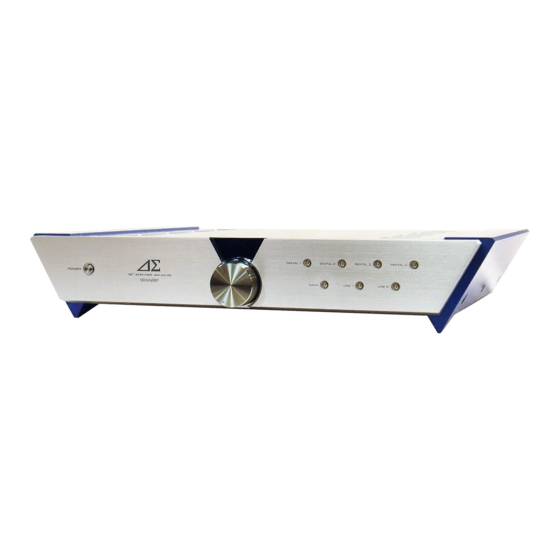
NAMES OF PARTS ........................................................................................................................................................... 3
OPERATION MANUAL ...................................................................................................................................................... 6
DISASSEMBLY .................................................................................................................................................................. 7
ADJUSTMENT ................................................................................................................................................................. 10
INTRODUCTION OF CIRCUIT OUTLINE ....................................................................................................................... 12
EXPLANATION OF 1-BIT UNIT ....................................................................................................................................... 18
WIRING PROCESS DIAGRAM ....................................................................................................................................... 21
BLOCK DIAGRAM ........................................................................................................................................................... 24
NOTES ON SCHEMATIC DIAGRAM .............................................................................................................................. 26
TYPE OF TRANSISTOR AND DIODE ............................................................................................................................. 26
SCHEMATIC DIAGRAM/WIRING SIDE OF P.W.BOARD ............................................................................................... 27
WAVEFORMS OF CD CIRCUIT ...................................................................................................................................... 50
TROUBLESHOOTING ..................................................................................................................................................... 51
FUNCTION TABLE OF IC ................................................................................................................................................ 55
SERVICE MANUAL
CONTENTS
SHARP CORPORATION
- 1 -
SM-SX100
• In the interests of user-safety the set should be restored to its
original condition and only parts identical to those specified be
used.
This document has been published to be used
for after sales service only.
The contents are subject to change without notice.
SM-SX100
No. S3021SMSX100/
Page
Advertisement
Table of Contents

Related Manuals for Sharp SM-SX100


Summary of Contents for Sharp SM-SX100
-
Page 1: Table Of Contents
SM-SX100 SERVICE MANUAL No. S3021SMSX100/ SM-SX100 • In the interests of user-safety the set should be restored to its original condition and only parts identical to those specified be used. CONTENTS Page IMPORTANT SERVICE NOTES (FOR U.S.A. ONLY) ......................2 IMPORTANT SERVICE NOTES (FOR U.K. -
Page 2: Important Service Notes (For U.s.a. Only)
SM-SX100 FOR A COMPLETE DESCRIPTION OF THE OPERATION OF THIS UNIT, PLEASE REFER TO THE OPERATION MANUAL. IMPORTANT SERVICE NOTES (FOR U.S.A. ONLY) BEFORE RETURNING THE AUDIO PRODUCT (Fire & Shock Hazard) Before returning the audio product to the user, perform the following safety checks. -
Page 3: Specifications
SM-SX100 SPECIFICATIONS Output terminals: Rated output power: RMS; 100 W + 100 W (DIN 45 500) DIGITAL OUT; Square type optical LINE OUT; RCA analog Total harmonic distortion: 0.02 % (1 kHz, 1 W) SPEAKERS; 8 ohms/4 ohms selectable Power source/power consumption:... - Page 4 SM-SX100 – 4 –...
- Page 5 SM-SX100 – 5 –...
-
Page 6: Operation Manual
SM-SX100 OPERATION MANUAL – 6 –... -
Page 7: Disassembly
SM-SX100 DISASSEMBLY Caution on Disassembly (D1)x3 Follow the below-mentioned notes when disassembling ø3x8mm the unit and reassembling it, to keep it safe and ensure Front Panel (B1)x6 excellent performance: (A1)x2 ø4x12mm 1. Be sure to remove the power supply plug from the wall ø4x12mm... - Page 8 SM-SX100 (T1)x4 (H1)x6 (G1)x3 ø3x12mm ø3x8mm (G1)x4 (T1)x2 ø3x6mm (H1)x5 ø3x6mm ø3x12mm (T1)x7 ø3x6mm (G1)x3 ø3x6mm ø3x6mm (J1)x4 ø3x8mm Bottom Panel (J1)x3 ø3x6mm (H1)x1 ø3x6mm Main Chassis Rear Panle Figure 8-4 Shield Shield (K2)x4 Cover A Cover B (M3)x1 Shield...
- Page 9 SM-SX100 Note 1: Positioning the volume joints 1. Rotate the sub volume shaft (inside of the set) so that the flat side faces upward. Fasten the joints in numerical order as shown in the in the figure. 2. Rotate anticlockwise both the main and sub shafts to mini- mum level.
-
Page 10: Adjustment
SM-SX100 ADJUSTMENT Measure the noise distribution between the set output terminals (Lch+, Lch- and Rch+, Rch-), and adjust VRA1 to VRA4. The VRA adjustment sequence is the same as that of the offset voltage adjustment. Measuring instrument: Yokokawa Electric brand SA2400 Measurement range : Refer to Fig. - Page 11 SM-SX100 1-bit PWB adjusting method Connect as shown Fig. 11-1. AC IN 110-120, 220-240, 230V AC POWER SUPPLY Digital Multimeter UNIT Oscilloscope Figure 11-1 [Simplified offset voltage adjustment] Connect the digital multimeter to the terminals of the speaker, and adjust the voltage between + and - of each terminal to 0 ± 10mV.
-
Page 12: Introduction Of Circuit Outline
SM-SX100 INTRODUCTION OF CIRCUIT OUTLINE 1. Technical background 1-1) Concept of coding technology Though the PCM system is the most popular method to convert the analog audio signals into the digital codes, the basic concept of the PCM system is that the signals are sampled with the frequencies whose band is two or more times of the frequency band to be transferred and is quantized into the multi-bits. - Page 13 SM-SX100 1-2) Application development of 1-bit coding technology The technology has been applied in the field of AD/DA conversion device, and it is well known that " modulation" is done in the intermediate process of the analog signal and multi-bit signal.
- Page 14 SM-SX100 "1" Area Integrator output : Lateral bar of thick line (-): 1 Lateral bar of doubled line (=): 0 ANALOG 0v- Analog signal waveform "0" Area 1 0 1 0 1 0 0 0 1 0 0 0 0 1 0 0 0 0 0 0 0 0 1 0 1 0 1 1 0 1 1 1 1 1 0 1 1 1 0 1 1 1 1 1 1 1 1 1 1 1 1 1 1 0 1 0 1...
- Page 15 SM-SX100 2-2) 7th order modulation circuit and devising If any 1-bit signal is produced through the operation of the modulation, the quantized noise is expelled to the high range. This is well known as "noise shaping", and it is used to reduce the quantized noise of the target frequency band (example: audible band).
- Page 16 "PWM signal" which has the analog width in the time axis direction is generally used as the signal to control the switching. The operational principle of Class D amplifier is developed to apply the said 7th order modulation 1-bit signal to the signal which controls the signal. Thus, the 1-bit amplifier "SM-SX100" is introduced. Line 1 (RCA PIN) Line 2 (Canon)
- Page 17 SM-SX100 3-2) The feature of 1-bit amplifier As described above, the amplification principle whose viewpoint is different from that of the existing analog amplifying circuit assures S/N in the audible band, thus achieving the audio amplification which has the wider band.
-
Page 18: Explanation Of 1-Bit Unit
SM-SX100 EXPLANATION OF 1-BIT UNIT modulation 1-bit conversion circuit The analog signals input from CNPA1 and CNPA2 are input from the terminals 17 and 20 of ICA1. At the input step of ICA1, the signal input signal is regarded as the differential input signal, and the switching signal which is later called "dynamic feedback"... - Page 19 SM-SX100 17/20 NF(+) 14/23 Integrator/Adder Double width Comparator Group conversion 15/22 NF(–) Input Step Figure 19-1 MODULATION 1-BIT CONVERSION CIRCUIT Diode prevents from returning to Vs. Y point point Q2 is turned on, and the holding gate voltage is gained from C.
- Page 20 SM-SX100 R256 RLY106 Detection Resistor D107 Q116 DA119 2SC2412KR R180 2.7K R179 (VRN) 100K (VRN) Q201 To µ-com 2SA1037 KR CNP106 Pin 12 R201 IC904 R214 R207 100K (VRN) Pin 27 (VRN) R213 C204 (VRN) R233 R205 0.01 (VRN) 100K...
-
Page 21: Wiring Process Diagram
SM-SX100 WIRING PROCESS DIAGRAM Check the wiring process. Any lead CNP101 (4P), CNP102 (3P) or CMP109 (6P) does not interfere with the cement resistor or heat sink plate. Pin 9 lead form the 1-bit unit is inserted to Pin 9 lead form the 1-bit unit is inserted to... - Page 22 SM-SX100 Bundle the core wound on the lead line of AC inlet into the hole of the shown hole with the nylon band. When bundling, put the head of the nylon band in the set. The core mounting direction is as shown.
- Page 23 SM-SX100 As shown, bundle A after passing the doubly stacked upper core through the hole on the side of the bottom shield of 1-bit amplifier. Bundling on the hole on marked side. After the line is processed, the connectors CNWAM1B, CNWAM28, CNWAM1C and CNWAM2C must not be retained with the core or lead line.
-
Page 24: Block Diagram
SM-SX100 DIGITAL SIGNAL RLY101 J101 ANAROG SIGNAL SACD ANALOG Q102 J102 J103 DIG/ANA VOL601 RLY102 CHANGE DIG/ANA MAIN RLY601, CHANGE VOLUME Line1 RLY602 RLY201 J104 Q104 ANALOG RLY104 Q606, J106-1 IC101~ Q614, Q618, IC103 Line2 Q208 Q602 Q610, ANALOG Q604 Q608, AMP. - Page 25 SM-SX100 1BIT UNIT SECTION VRA1~VRA4 FEEDBACK CIRCUIT FEEDBACK LEVEL ADJUSTMENT SWITCHING LOGIC CIRCUIT ICA2 QA1~QA8 DIGITAL INPUT QA9~QA16 ICA4~ICA7 NAND GATE LOW PASS POWER ICA1 LEVEL SHIFT FET DRIVER 74AC00F FILTER 7TH ORDER HIP2100 SWITCHING ICA3 ANALOG AMP. ANALOG MODULATION...
-
Page 26: Notes On Schematic Diagram
SM-SX100 NOTES ON SCHEMATIC DIAGRAM • Resistor: • The indicated voltage in each section is the one measured To differentiate the units of resistors, such symbol as K and by Digital Multimeter between such a section and the chas- M are used: the symbol K means 1000 ohm and the symbol sis with no signal given. -
Page 27: Schematic Diagram/Wiring Side Of P.w.board
SM-SX100 LED903 LED901 LED902 GL9BC030 GL9BC030 GL9BC030 C904 R908 47/10 LED PWB-A11 LED904 R901 R909 LNG91LCF C902 AUX1 R916 (SACD) C903 LED905 R902 R910 10 11 12 13 14 15 16 17 18 10 11 12 13 14 15 16 17 18... - Page 28 SM-SX100 P33 12 - F TO DIGITAL PWB CNP808 CNS108 6 5 4 3 2 1 6 5 4 3 2 1 JACK PWB-A10(1/2) MAIN PWB-A1(1/3) BI108 MAIN VOLUME P R101 RLY101 L101 3.3K J101 CNP601 L-CH L103 MAIN R103...
- Page 29 SM-SX100 P30 1 - C P30 1 - B P31 12 - B P31 12 - G TO 1BIT AMP TO 1BIT AMP TO 1BIT AMP TO 1BIT AMP TO 1BIT AMP PWB P31 12 - E P31 12 - F...
- Page 30 SM-SX100 When it is touched with the tester, the relay is activated (oscillation is stopped.). CNWAM1A ANALOG IN L-CH CA86 RA70 TEST RA86 DGND_AD 1.5V 100K NFL1(+) GNDX AGND AGND_AD P29 9 - A 11.2896 CNWAM1B CNPA2 2.2V 1.5V NFL2(–)
- Page 31 SM-SX100 1BIT AMP.PWB–B ed.). ICA2 74AC00F CXA1 4.96V(0V) RESET 11.2896MHz NAND GATE 2.2V –B –22V 18P(CH) 1.3V CA21 BLA1 0.22 CA10 4.8V +5VA DGND_AD 0.22 18P(CH) CA13 BLA2 100/16 AGND_AD AGND P29 9 - A BLA6 BLA3 DGND CNP109 DGND_AD 2.5V...
- Page 32 SM-SX100 C819 22P(CH) C815 R834 R833 X801 47/10 120 R835 R821 11.2896MHz C820 C816 22P(CH) C825 IC820 C880 TC7WU04F 0.22 C823 PC CONTROL R826 RSTN/POR RSTN SKSY VDDA R817 R827 2.5V CTLN BCKI R828 2.5V R818 R819 2.5V 2.5V (NC) LRCI 3.3K...
- Page 33 SM-SX100 MAIN PWB-A1(3/3) DIGITAL PWB-A2 D651 DA119 Q651 2SC2412KR –15V –B R651 R845 R834 C654 R833 +32V 120 R835 0.01 R661 R657 C825 R653 C651 33/50 R655 IC651 – D652 NJM4558M DA119 RSTN/POR 2.5V MOTOR DRIVER R658 BCKI RSTN 2.5V IC806 2.5V...
- Page 34 SM-SX100 110-127V SOC501 AC SOCKET 120V,60Hz COR501 (305) TO MAIN CHASSIS CNS501 CNP501 SW501 R501 POWER 390K C501 0.33 CNW505 L502 L503 UNT503 C504 C503 AC DC CONVERTER 0.0022 0.0022 C502 0.33 L501 C530 0.0015 POWER FILTER PWB-C2 POWER PWB-C1...
- Page 35 SM-SX100 220-240V SOC501 When Servising, pay attention as the AC INLET area enclosed by this line( ) is AC 230V, 50Hz directly connection with AC main voltage. COR501 (305) TO MAIN CHASSIS CNS501 CNP501 R501 SW501 390K POWER C501 0.33...
-
Page 36: Top View
SM-SX100 P44 1 - A TO RELAY PWB CNS111A 1 2 3 4 5 6 7 CNS110A CNP808 R255 R655 CNP115 R254 R882 SWITCH2 R253 R659 R884 PWB-A5 RLY802 IC651 C653 R216 CNP110 R185 R661 C164 R215 R166 R146 R184... - Page 37 SM-SX100 P46 3 - D TO SYSTEM MICROCOMPUTER PWB CNP906 C820 C819 1 2 3 4 5 6 Q801 R870 P808 CNP804 IC807 CNP801 R882 R867 R884 C832 R825 C830 Q802 C863 C829 RLY802 IC820 C837 C839 IC801 C815 C835...
- Page 38 SM-SX100 C821 C824 R817 IC804 R819 R820 R830 L816 R892 IC810 C848 R851 DIGITAL PWB-A2(BOTTOM VIEW) : Through-hole where the top and bottom patterns are connected. Figure 38 WIRING SIDE OF P.W.BOARD (3/14) – 38 –...
-
Page 39: Bottom View
SM-SX100 OM VIEW) LINE2 PWB-A6 (BOTTOM VIEW) MAIN PWB-A1(BOTTOM VIEW) Figure 39 WIRING SIDE OF P.W.BOARD (4/14) – 39 –... - Page 40 SM-SX100 110-127V CNS502 P49 8 - B CNP502 TO POWER FILTER UDC+ UNIT503 L2/N UDC- BUSOK SW501 POWER ON – OFF CNS503 CNW503 R506 C524 C523 C522 –IN OUT– C521 L509 GATE OUT –S C508 TRIM L506 GATE IN FIL502...
- Page 41 SM-SX100 POWER PWB-C1(BOTTOM VIEW) Figure 41 WIRING SIDE OF P.W.BOARD (6/14) – 41 –...
- Page 42 SM-SX100 220-240V When Servicing, pay attension as the area enclosed by this line ) is directry connected with AC main voltage. CNS502 P49 8 - B CNP502 TO POWER FILTER UDC+ UNIT503 L2/N UDC- BUSOK SW501 POWER ON – OFF...
- Page 43 SM-SX100 POWER PWB-C1(BOTTOM VIEW) Figure 43 WIRING SIDE OF P.W.BOARD (8/14) – 43 –...
- Page 44 SM-SX100 P36 3 - A TO MAIN PWB CNP11 CNS111A 1 2 3 4 5 6 7 1 2 3 4 5 6 7 CNS111B D109 D108 TA101 TA102 SPEAKER TERMINAL L-CH R-CH RELAY PWB-A7 (BOTTOM VIEW) <How to process the wire of the core>...
- Page 45 SM-SX100 1BIT AMP PWB-B (BOTTOM SIDE FROM TOP VIEW) L-CH(+) L-CH(-) R-CH(-) R-CH(+) RA804 RA803 RA802 RA801 CA802 CA804 CA803 CA801 RELAY PWB-A7 (TOP VIEW) DA10 DA13 RA104 RA103 RA101 CA46 CA48 CA49 RA102 QA10 QA14 QA13 DA11 DA12 DA16...
- Page 46 SM-SX100 SWITCH1 PWB-A4 (TOP VIEW) COLOR TABLE SW904 BROWN DIGITAL4 R938 R945 R D ( R ) R937 R944 ORANGE R943 YELLOW R936 SW907 GREEN LINE2 BLUE VIOLET GRAY SW903 W H ( W ) WHITE DIGITAL3 BLACK PINK SW906...
- Page 47 SM-SX100 AUX1 AUX2 AUX3 (SACD) (LINE1) (LINE2) CNP901 R909 R910 LED904 LED905 LED906 R911 R901 R902 R903 R914 R913 R905 R906 R904 R907 R915 LED909 LED908 R912 LED910 LED907 DIG1 DIG2 DIG3 DIG4 (ST) (BNC) (TOS) (COAX) LED PWB-A11 L-CH...
- Page 48 SM-SX100 SWITCH1 PWB-A4 (BOTTOM VIEW) SYSTEM MICROCOMPUTER PWB-A3(BOTTOM VIEW) MAIN VOLUME PWB-A9 JACK PWB-A10(BOTTOM VIEW) (BOTTOM VIEW) : Through-hole where the top and bottom patterns are connected. Figure 48 WIRING SIDE OF P.W.BOARD (13/14) – 48 –...
- Page 49 SM-SX100 110-127V POWER FILTER PWB-C2(TOP VIEW) L502 C530 CNP502 P40 5 - A CNS502 L501 C502 TO UNT503 C501 TO MAIN CHASSIS (305) CNP501 CNS501 L503 SOC501 F501 AC SOCKET 7A/125V 120V,60Hz COR501 220-240V POWER FILTER PWB-C2(TOP VIEW) L502 C530...
-
Page 50: Waveforms Of Cd Circuit
SM-SX100 WAVEFORMS OF CD CIRCUIT • OUTR(+), OUTR(-) • QA1, QA5 • OUTL(+), OUTL(-) • QA2, QA6 • QA3, QA7 Observe • QA4, QA8 each pair. OUTR(+), Observe (OUTL(+)) each pair. (QA2, 3, 4) COLECTOR OUTR(-), (OUTL(-)) (QA6, 7, 8) COLECTOR •... -
Page 51: Troubleshooting
SM-SX100 TROUBLESHOOTING (LED does not come on and it does not sound.) • Power is not supplied. • Check the fuse F501. Does AC100V stand between Pins 1 and 2 of the power • Check the parts on the power filter PWB. - Page 52 SM-SX100 • It does not sound at the analog input (Line 1 and Line 2) alone. Check the wiring from the input terminal to CNP116 and Is any signal input to CNP116 or CNP117? CNP117. Does it not sound on both Line 1 and Line 2? Check the wiring from RLY101, RLY102, RLY104 and the relays to the microcomputer IC904.
- Page 53 SM-SX100 From the front page Is any 1-bit signal from Pins 27 and 33 of IC807 output Check IC808, IC809, IC811, IC812 and IC813. to RLY801? Does RLY801 and RLY802 operate? Check the operation of Q801 and Q802 and the wiring of each to the microcomputer IC904.
- Page 54 SM-SX100 • 1-bit amplifying section check (power trouble/protector activation) Don't the protector activate together with drop of voltage Recheck the main body section. ±32V if CNWAM4 and CNWAM3 are disconnected? Does the oscillating circuit operate? Check Pin 9. Replace ICA1.
-
Page 55: Function Table Of Ic
SM-SX100 FUNCTION TABLE OF IC IC804 VHiYM3436D/-1: Digital Interface Receiver (YM3436D) • Outline YM3436D(DIR2) is a LSI which receives and demodulate the digital/audio/interface/format signals which comply with EIAJ CP- 340 and AES/EBU. Keeping the features of the existing YM3623B(DIR), it is designed to not only strengthen the external synchronization, error process and other functions but also be more general for the channel status, user data output and other general applications. - Page 56 SM-SX100 IC804 VHiYM3436D/-1: Digital Interface Receiver (YM3436D) 25 28 MCA,MCB,MCC, EXTW WC,SYNC,OPT System Clock Timing Generator RSTN DDIN Data Clock TSTN EIAJ(AES/EBU) Control TST2 Digital Audio Interface Decoder FS1,0 Asynchronous Buffer (1 word per each of DOUT Microcomputer Interface L and R)
- Page 57 SM-SX100 IC806 VHiSM5844AF-1: Sampling Rate Converter (SM5844AF) (1/2) • Outline SM5844AF is a special LSI for sampling rate converter, having a function to asynchronously covert the sample rate of the digital audio signal. The input/output interface correspond to the input data of 16/20-bit word length and the output data of 16/18/20-bit word length.
- Page 58 SM-SX100 IC806 VHiSM5844AF-1: Sampling Rate Converter (SM5844AF) (2/2) Pin No. Port Name Input/Output Function 34, 35 SLAVE Input with pull-up resistor Mode setting of BCKO, LRCO terminal. H: Output terminal is selected. (Slave mode) L: Input terminal is selected. (Master mode)
- Page 59 SM-SX100 IC807 VHiTDA1307/-1: 1-Bit Conversion (TDA1307) (1/2) • Outline The TDA1307 is an advanced oversampling digital filter employing bitstream conversion technology, which has been designed for use in premium performance digital audio applications. Audio data is input to the TDA1307 through its multiple-format interface.
- Page 60 SM-SX100 IC807 VHiTDA1307/-1: 1-Bit Conversion (TDA1307) (2/2) Pin No. Port Name Input/Output Function Input (Note 2) Clock input, to be generated by the microprocessor — Ground 1 — Supply voltage 2 Input (Note 2) Command/peak data request line Notes 1. These pins are configured as internal pull-down.
- Page 61 SM-SX100 IC901~IC903 VHiBU2114F+-1: LED Driver (BU2114F) • Outline It is the low power consuming CMOSIC which has the latch in the 8-bit shift register and can asynchronously latch the data latched in the shift register. Since the output (O1 to O8) is the open drain output (Since the protective diode is not provided, the voltage of VDD or more to max.
- Page 62 SM-SX100 IC904 RH-iX2816AFZZ: System Microcomputer (IX2816AF) Pin No. Port Name Terminal Name Input/Output Function LED3, P83 DATA_IN Input External IC communication input LED2, P82 DATA_OUT Output External IC communication output LED1, P81 IC_CLK Input External IC communication clock LED0, P80 —...
- Page 63 SM-SX100 IC904 RH-iX2816AFZZ: System Microcomputer (IX2816AF) AUX3 LED3,P83 DATA-IN DIG_MUTE LED2,P82 DATA-OUT DIG_A LED1,P81 IC_CLK DIG_B LED0,P80 IC_STB AN0,PA0 P22,IRQ2 MN101C117ßF P_IN AN1,PA1 P21,IRQ1,SENS VOLDIS PROTECT AN2,PA2 P20,IRQ0 KEYA D DATA AN3,PA3 P14,TM4IO KEYB D LATCH AN4,PA4 KEYC P13,TM3IO D CLK...
- Page 64 SM-SX100 ICA1 RH-iX2815AFZZ: 7TH ORDER MODULATION CONVERSION LSI (IX2815AF) Pin No. Port Name Input/Output Function VDDR — R channel digital output section power terminal OUTR (+) Output R channel forward output terminal OUTR (–) Output R channel reverse output terminal GNDD —...
-
Page 65: Parts Guide
“HOW TO ORDER REPLACEMENT PARTS” To have your order filled promptly and correctly, please furnish the For U.S.A. only following information. Contact your nearest SHARP Parts Distributor to order. 1. MODEL NUMBER 2. REF. No. 3. PART NO. 4. DESCRIPTION For location of SHARP Parts Distributor, Please call Toll-Free;... -
Page 66: Integrated Circuits
SM-SX100 PRICE PRICE PARTS CODE DESCRIPTION PARTS CODE DESCRIPTION RANK RANK INTEGRATED CIRCUITS D503,504 VHDRK36++++-1 AE FET,DRK36 D505 VHD1SS133//-1 AA Silicon,1SS133 D601,602 VHDDA119///-1 AA Silicon,DA119 IC101~104 RH-IX2838AFZZ AP Analog Amp.,IX2838AF D651,652 VHDDA119///-1 AA Silicon,DA119 [110-127V] D801 VHD1SS133//-1 AA Silicon,1SS133 IC101~104 VHIOPA2134/-1 AS Analog Amp.,OPA2134... - Page 67 SM-SX100 PRICE PRICE DESCRIPTION PARTS CODE DESCRIPTION PARTS CODE RANK RANK AN 270 µF,16V,Electrolytic AC 47 µF,10V,Electrolytic C132 RC-EZ1687AFZZ C904 RC-EZ1692AFZZ AD 100 µF,50V,Electrolytic AC 10 µF,16V,Electrolytic C133 RC-EZ1689AFZZ C905 RC-EZ1685AFZZ AC 1 µF,16V AA 0.1 µF,25V C134 VCKYTQ1CF105Z C906 VCKYTV1EB104K AN 270 µF,16V,Electrolytic...
- Page 68 SM-SX100 PRICE PRICE PARTS CODE DESCRIPTION PARTS CODE DESCRIPTION RANK RANK R238~241 VRN-TV2AS271D AA 270 ohms,1/10W R949 VRS-TV2AB222J AA 2.2 kohms,1/10W R242,243 VRN-TV2AS152D AA 1.5 kohms,1/10W R950 VRS-TV2AB392J AA 3.9 kohms,1/10W R244 VRN-TV2AS472D AA 4.7 kohms,1/10W R951 VRS-TV2AB562J AA 5.6 kohms,1/10W...
- Page 69 SM-SX100 PRICE PRICE DESCRIPTION PARTS CODE DESCRIPTION PARTS CODE RANK RANK CNW502 QCNWN6893AFZZ J Connector Ass’y,3Pin [110-127V] LANGQ1217AFFQ AV Bracket,Erase A CNW504A,B QCNWN6774AFZZ J AS Connector Ass’y,2Pin LANGQ1218AFFQ AW Bracket,Erase B CNW810 QCNWN6879AFZZ J Lug Wire LANGT1968AFFW AT Bracket,Power Switch CNWAM1A/B/C QCNWN6790AFZZ J AS Connector Ass’y,4/2/2Pin...
- Page 70 SM-SX100 PRICE PRICE PARTS CODE DESCRIPTION PARTS CODE DESCRIPTION RANK RANK PSHEF0274AFZZ AF Sheet,Spacer B QACCE0106AFZZ AW AC Power Supply Cord PSPAG0268AFZZ AF Cushion,Spacer [Except for U.K./Singapore/ PFLT-1165AFZZ AF Felt Hong Kong/Switzerland/U.S.A./ PSPAZ0596AFZZ AD PWB Spacer C Canada] TLABZ2606AFZZ Label,Earth...
- Page 71 SM-SX100 603x2 645x2 601x6 607x3 601x2 645x2 603x2 638x4 607x3 TA102 606x13 TA101 638x4 621x2 SOC501 603x4 603x4 603 603 627x4 J107,108 603x3 627x3 606x13 J801 J106 with 309x2 TA101,102 J101 627x2 ~104 627x8 SW501 618x4 219x4 PWB-A6 603x2 J802...
- Page 72 SM-SX100 624x2 630x2 603x6 624x2 624x2 630x2 630x2 624x2 603x2 630x2 624x2 603 236x3 612x2 613x6 639x7 632x6 644x2 612x2 612x2 608x2 613x6 632x6 644x2 608x2 639x3 612x2 262x2 289x4 234x2 UNT501 611x3 283x4 UNT502 283x4 262x3 UNT503 QA14 288x4...
- Page 73 SM-SX100 603x2 PWB-A2 615x5 615x3 308x2 615x3 PWB-C2 615x4 294x2 301x3 PWB-A7 603x6 276x5 630x5 VOL601 621x2 Q115 Q114 IC108 with PWB-A9 VOL601 259x2 615x6 634x2 634x2 278x4 PWB-A1 284x3 234x2 277x2 236x4 234x2 277x13 603x4 602x22 236x4 603x4 603x3...
- Page 74 SM-SX100 PACKING METHOD (FOR U.K. ONLY) Setting position of switches and knobs VOLUME IMPEDANCE SELECTOR 4 ohms 1. AC Power Supply Cord QACCB0113AFZZ 10. Operation Manual TiNSM0160AFSA 2. Packing Add., Bottom SPAKA2740AFZZ 11. Spacer, Speaker Terminal PSPAS0278AFZZ 3. Packing Add., Top SPAKA2741AFZZ 12.
- Page 75 SM-SX100 PACKING OF THE SET (FOR U.S.A. ONLY) Setting position of switches and knobs VOLUME IMPEDANCE SELECTOR 4 ohms GLEGG0124AF00 SSAKA2343QCZZ Sheet,Leg TGANE1220AFZZ Polyethylene Bag, Warranty Card Accessories GDAi-3053AFFC Leg Base,Front GDAi-3054AFFC PSPAS0278AFZZ Leg Base,Rear Spacer,Speaker Terminal TiNSM0160AFSA SPAKZ0544AFZZ Operation Manual...
- Page 76 SM-SX100 © COPYRIGHT 2000 BY SHARP CORPORATION ALL RIGHTS RESERVED. No part of this publication may be reproduced, stored in a retrieval system, or transmitted in any from or by any means, electronic, mechanical, photocopying, recording, or otherwise, without prior written permission of the publisher.