
Related Manuals for Atmel AVR STK500


Summary of Contents for Atmel AVR STK500
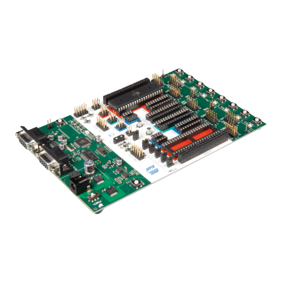
- Page 1 STK500 ....................User Guide...
-
Page 3: Table Of Contents
Clock Settings, XTAL1 and OSCSEL ..........3-20 3.8.5 BSEL2 Jumper .................3-22 3.8.6 PJUMP Jumpers................3-22 Expansion Connectors ................3-23 3.9.1 Signal Descriptions................3-25 3.10 Prog Ctrl and Prog Data Headers ............3-25 3.11 Miscellaneous ..................3-26 3.11.1 RESET Push Button .................3-26 3.11.2 PROGRAM Push Button ..............3-27 AVR STK500 User Guide 1925C–AVR–3/03... - Page 4 In-System Programming of an External Target System ....... 6-1 Section 7 Troubleshooting Guide ................. 7-1 Section 8 Technical Support................. 8-1 Section 9 Example Applications ................9-1 Using LEDs and Switches.................9-1 Section 10 Appendix A ..................10-1 AVR STK500 User Guide 1925C–AVR–3/03...
-
Page 5: Introduction
Kit. The STK500 is a complete starter kit and development system for the AVR Flash Microcontroller from Atmel Corporation. It is designed to give designers a quick start to develop code on the AVR and for prototyping and testing of new designs. -
Page 6: Device Support
1. In external target or in STK501, devices do not fit into the sockets of STK500. Support for new AVR devices may be added in new versions of AVR Studio. The latest version of AVR Studio is always available from www.atmel.com. AVR STK500 User Guide 1925C–AVR–3/03... -
Page 7: Getting Started
– (1 pc) 6-wire cable for In-System Programming – (4 pcs) 2-wire cable for UART and DataFlash connections n 9-pin RS-232 cable n DC power cable n Atmel CD-ROM with datasheets and software n AT90S8515-8PC sample microcontroller System The minimum hardware and software requirements are:... -
Page 8: Quick Start
The starter kit can be configured for various clock and power sources. A complete description of the jumper settings is explained in paragraph 3.8 on page 3-15 and on the reverse side of the starter kit. AVR STK500 User Guide 1925C–AVR–3/03... -
Page 9: Connecting The Hardware
LED will turn green. If programming fails, the LED will turn red after programming. See the troubleshooting guide in Section 7 on page 7-1. AVR STK500 User Guide 1925C–AVR–3/03... - Page 10 Getting Started Figure 2-3. AVR Studio STK500 Programming Menu Complete descriptions of using the STK500 interface in AVR Studio are given in Section 5 on page 5-1. AVR STK500 User Guide 1925C–AVR–3/03...
-
Page 11: Hardware Description
1. Confirm that this is connected to pin 1 on each of the headers. Figure 3-2 shows how the LED control is implemented. This solution will give the same amount of light from the LED for all target voltages from 1.8V to 6.0V. AVR STK500 User Guide Rev. 1925C–AVR–3/03... -
Page 12: Description Of User Switches
In the STK500 design, we have added an external 10K pull-up to give all users a logical “1” on SWn when the push-button is not pressed. The 150R resistor limits the current going into the AVR. AVR STK500 User Guide 1925C–AVR–3/03... -
Page 13: Connection Of Leds And Switches
1. Figure 3-5. General Pinout of I/O Port Headers PORTx The PORTE/AUX header has some special signals and functions in addition to the PORTE pins. The pinout of this header is shown in Figure 3-6. AVR STK500 User Guide 1925C–AVR–3/03... - Page 14 Figure 3-8. The square marking indicates pin 1. Figure 3-7. Pinout of the Switch Header SWITCHES Figure 3-8. Pinout of the LED Header LED0 LED1 LED2 LED3 LED4 LED5 LED7 LED6 LEDS AVR STK500 User Guide 1925C–AVR–3/03...
-
Page 15: Description Of User Rs-232 Interface
UART pins to the RS-232. The connection is shown in Figure 3-9. The block schematic of the RS-232 connection is shown in Figure 3-10. Figure 3-9. Connection of I/O Pins to UART Figure 3-10. Schematic of UART Pin Connections 470R 470R RS-232 MAX202CSE Voltage Converter AVR STK500 User Guide 1925C–AVR–3/03... -
Page 16: Description Of Dataflash Pins
A DataFlash is a high-density Flash memory with SPI serial interface. A detailed DataFlash Pins datasheet of the DataFlash can be obtained from the Flash memory section of the Atmel CD-ROM or from the Atmel web site. The DataFlash can be connected to the I/O pins of the microcontroller sockets. The 4-pin header marked “DATAFLASH”... - Page 17 Hardware Description Figure 3-13. Connection of I/O Pins to DataFlash for AT90S8515 Figure 3-14. Schematic of DataFlash Connections Voltage AT45D021 Converter DataFlash AVR STK500 User Guide 1925C–AVR–3/03...
-
Page 18: Target Socket Section
Four general nets (VTARGET, RESET, XTAL1 and AREF) can be connected to the socket section. The following sections describe how to use both programming methods. For instructions on using the AVR Studio programming software, see Section 5, “Using AVR Studio” on page 5-1. AVR STK500 User Guide 1925C–AVR–3/03... -
Page 19: Isp Programming
SCKT3400D1 and SCKT3400D1 are connected to PB5. The RESET signal used during ISP programming is therefore not connected to pin 1 on these sockets. This signal must be connected by placing a wire between RST and the PORTE header and PB5 on the PORTB header. AVR STK500 User Guide 1925C–AVR–3/03... - Page 20 6-wire cable is connected from the ISP6PIN header to the red SPROG3 target ISP header, and the AT90S2313 part is inserted in the red socket marked “SCKT3100D3”. Figure 3-16. Example Connection for Programming AT90S2313 SPROG1 SPROG2 SCKT3300D3 SPROG3 ISP6PIN 3-10 AVR STK500 User Guide 1925C–AVR–3/03...
-
Page 21: High-Voltage Programming
PJUMP jumpers and mount BSEL2 terminal to PC2. See Section 3.8.5 and Section 3.8.6. AT90S2323 SCKT3400D1 Blue Serial High-voltage Programming AT90S2343 ATtiny11 ATtiny12 ATtiny22 ATtiny15 SCKT3600A1 Blue SCKT3700A1 Blue Socket not in use in this version of STK500 AVR STK500 User Guide 3-11 1925C–AVR–3/03... - Page 22 Figure 3-17. Figure 3-17. Connection for Parallel High-voltage Programming Some of the jumper settings on STK500 must be changed when using High-voltage Pro- gramming. Figure 3-18 explains these jumper settings. 3-12 AVR STK500 User Guide 1925C–AVR–3/03...
- Page 23 12. Ensure that VTARGET is between 4.5V and 5.5V before programming. See Sec- tion 5.3.5.1. For a complete description of jumper settings, see Section 3.8, “Jumper Settings”. Note: Remove the hardware setup for High-voltage Programming before starting a debug session. AVR STK500 User Guide 3-13 1925C–AVR–3/03...
- Page 24 DATA1 pin (pin 2) on the PROG DATA header. 10. Switch power on and you are ready to program. All connections are shown in Figure 3-19. Figure 3-19. Connection for Serial High-voltage Programming 3-14 AVR STK500 User Guide 1925C–AVR–3/03...
-
Page 25: Jumper Settings
XTAL1 On-board Clock System connected OSCSEL On-board Oscillator selected BSEL2 Unmounted. Used for High-voltage Programming of ATmega8, ATmega16, ATmega161, ATmega163, ATmega128, and ATmega323 PJUMP Unmounted. Used for High-voltage Programming of AT90S2333, AT90S4433, and ATmega8 AVR STK500 User Guide 3-15 1925C–AVR–3/03... -
Page 26: Target V
Regulator Green LED Jumper Master Note: The green LED will light when there is a voltage available on the VTG NET. It’s impossible to use the debug or programming area of STK500 without VTG. 3-16 AVR STK500 User Guide 1925C–AVR–3/03... -
Page 27: Analog Reference Voltage, Aref
PWM. The AVR’s AREF signal is also accessible on the PORTE header; this pin can also be used for external AREF signal. Figure 3-24 shows the internal connec- tion of the AREF signal. AVR STK500 User Guide 3-17 1925C–AVR–3/03... -
Page 28: Reset Settings, Reset
When using an external reset system, it must allow the reset line to be controlled by the master microcontroller reset system during programming. The RESET button is disconnected if the RESET jumper is not mounted. Figure 3-25 explains the RESET jumper options. 3-18 AVR STK500 User Guide 1925C–AVR–3/03... - Page 29 Jumper RESET PORTE/AUX Note: During High-voltage Programming, STK500 applies 12V to the AVR’s RESET line. Thus, an external reset circuit not capable of handling this must be discon- nected before High-voltage Programming the AVR. AVR STK500 User Guide 3-19 1925C–AVR–3/03...
-
Page 30: Clock Settings, Xtal1 And Oscsel
RESET XTAL1 OSCSEL On-board XTAL1 Signal Disconnected When the XTAL1 jumper is not mounted, an external clock source or crystal can be con- nected to the PORTE header. This is shown in Figure 3-30. 3-20 AVR STK500 User Guide 1925C–AVR–3/03... - Page 31 The long signal lines in this system makes it difficult to drive a crystal with the On-chip Oscillators on the AVR. The oscillator on STK500 is designed to operate on all target voltages from 1.8 to 6.0V. AVR STK500 User Guide 3-21 1925C–AVR–3/03...
-
Page 32: Bsel2 Jumper
PJUMP jumpers should only be mounted when using High-voltage Programming on AT90S2333, AT90S4433, or ATmega8. During debugging, High-voltage Programming of other parts and ISP programming, these jumpers should not be mounted. Figure 3-32. PJUMP Jumpers Placement Correct Jumper Placement Correct 3-22 AVR STK500 User Guide 1925C–AVR–3/03... -
Page 33: Expansion Connectors
STK500. The pinout of the expansion connectors is shown in Figure 3-34 and Fig- ure 3-35. Figure 3-33. Expansion Headers Expansion Header 0 Prog Ctrl Pin 1 Pin 1 Expansion Header 1 Prog Data AVR STK500 User Guide 3-23 1925C–AVR–3/03... - Page 34 Hardware Description Figure 3-34. Expansion Connector 0 Pinout AUXI0 AUXO0 BSEL2 Figure 3-35. Expansion Connector 1 Pinout AUXI1 AUXO1 DATA7 DATA6 DATA5 DATA4 DATA3 DATA2 DATA1 DATA0 3-24 AVR STK500 User Guide 1925C–AVR–3/03...
-
Page 35: Signal Descriptions
The Prog Ctrl signals are normally used for the control signals when parallel High- voltage Programming an AVR device. Note: All Prog Ctrl signals are based on 5V CMOS logic. No voltage conversion to adapt to VTG is done on these signals. AVR STK500 User Guide 3-25 1925C–AVR–3/03... -
Page 36: Miscellaneous
The RESET push button resets the target AVR device when pushed. The master micro- controller is not controlled by the RESET push button. When the RESET jumper is not mounted, the RESET push button is disabled. 3-26 AVR STK500 User Guide 1925C–AVR–3/03... -
Page 37: Program Push Button
LED will turn red to indicate that programming failed. When programming fails, check the troubleshooting guide in Section 7 on page 7-1. During start-up, the sta- tus LED will shift from red, through yellow, to green to indicate that the master microcontroller is ready. AVR STK500 User Guide 3-27 1925C–AVR–3/03... - Page 38 Hardware Description 3-28 AVR STK500 User Guide 1925C–AVR–3/03...
-
Page 39: Installing Avr Studio
AVR development. It has an editor, an assembler and a debugger and is front-end for all AVR emulators and the STK500 starter kit. To install AVR Studio, insert the supplied Atmel CD-ROM databook in the computer and navigate to “Products → AVR 8-bit RISC → Software”. Right-click with the mouse on the “AVRstudio.exe”... - Page 40 Installing AVR Studio AVR STK500 User Guide 1925C–AVR–3/03...
-
Page 41: Using Avr Studio
Section 4 on page 4-1. Once installed, AVR Studio can be started by double- Software clicking on the AVR Studio icon. If default install options are used, the program is located in the Windows “Start menu → Programs → Atmel AVR Tools” folder. 5.2.1 Starting STK500 Pressing the “AVR”... -
Page 42: Stk500 User Interface
“Input HEX File” option. Browse to the correct file by pressing the button or type the complete path and filename in the text field. The selected file must be in “Intel-hex” for- mat or “extended Intel-hex” format. Figure 5-2. Program AVR STK500 User Guide 1925C–AVR–3/03... -
Page 43: Fuses" Settings
(i.e., pressing “Chip Erase” button in the “Program” settings). Detailed information on what fuses are available in the different programming modes and their functions can be found in the appropriate device datasheet. Figure 5-3. Fuses AVR STK500 User Guide 1925C–AVR–3/03... -
Page 44: Lockbits" Settings
The signature bytes act like an identifier for the part. After reading the signature, the software will check if it is the correct signature according to the chosen device. Please refer to the AVR datasheets to read more about signature bytes. AVR STK500 User Guide 1925C–AVR–3/03... -
Page 45: Board" Settings
The interface is very flexible and it is possible to force the operating conditions beyond the recommended specifications for the device. Doing this is not recommended, and may damage the target device. The recommended operating conditions for the part are stated in the device datasheet. AVR STK500 User Guide 1925C–AVR–3/03... - Page 46 It is not possible to set AREF to a higher voltage than VTARGET because this will per- manently damage the AVR. The physical connection of the AREF voltage is shown in Figure 3-24 on page 3-18. AVR STK500 User Guide 1925C–AVR–3/03...
-
Page 47: Auto" Settings
“Program” settings. All commands depend on and use the settings given in the STK500 user interface. Figure 5-7. Auto It is possible to log the command execution to a text file by checking the “Log to file” check box. AVR STK500 User Guide 1925C–AVR–3/03... -
Page 48: History Window
The History window is located at the bottom of the STK500 view. In this window the dia- log between AVR Studio and STK500 is shown. For every new command performed, the old dialog is replaced with the new one. Figure 5-8. History Window AVR STK500 User Guide 1925C–AVR–3/03... -
Page 49: Command Line Software
Verify device; FLASH (f), EEPROM (e) or both (b). Can be used with -p or stand alone. Corresponding input files are required. Set lock byte. “value' is an 8-bit hex. value. Verify lock byte. “value” is an 8-bit hex. value to verify against. Read back lock byte. AVR STK500 User Guide 1925C–AVR–3/03... - Page 50 Help information (overrides all other settings) Figure 5-9. Sample Usage Program Flash Erase before Program Name of hex File stk500 -dAT90S8515 -iftest.hex Select Device Number Verify Device Serial Programming Mode 5-10 AVR STK500 User Guide 1925C–AVR–3/03...
-
Page 51: In-System Programming Of An External Target System
If the other application has its own power supply to VTG, the jumper VTARGET must be removed before connecting STK500 to the other application. STK500 may be damaged if the VTARGET jumper is not removed. AVR STK500 User Guide Rev. 1925C–AVR–3/03... - Page 52 In-System Programming of an External Target System AVR STK500 User Guide 1925C–AVR–3/03...
-
Page 53: Troubleshooting Guide
ISP6PIN header to the correct SPROG target ISP header (page 3-10). The jumpers settings are Set jumper to default setup wrong. (page 3-15). The memory lock bits are Erase the memory before programmed. programming. AVR STK500 User Guide Rev. 1925C–AVR–3/03... - Page 54 0.3V in AVR Studio. turned off. The LEDs don’t work STK500 must be powered for Supply poser to STK500 and (running from external LEDs to work. turn it on. VTARGET). AVR STK500 User Guide 1925C–AVR–3/03...
-
Page 55: Technical Support
Section 8 Technical Support For technical support, please contact avr@atmel.com. When requesting technical sup- port for STK500, please include the following information: n Version number of AVR Studio. This can be found in the AVR Studio menu, “Help → About”. - Page 56 Technical Support AVR STK500 User Guide 1925C–AVR–3/03...
-
Page 57: Example Applications
; Set PORTB to output ;**** Test input/output LOOP: PORTB,temp ; Update LEDS sbis PIND,0x00 ; If (Port D, pin0 == 0) Temp ; then count LEDS one down sbis PIND,0x01 ; If (Port D, pin1 == 0) AVR STK500 User Guide Rev. 1925C–AVR–3/03... - Page 58 ; If (Port D, pin6 == 0) swap Temp ; then swap nibbles of LEDS ;**** Now wait a while to make LED changes visible. DLY: Delay brne Delay2 brne rjmp LOOP ; Repeat loop forever AVR STK500 User Guide 1925C–AVR–3/03...
- Page 59 RESET STATUS SYSTEM PORT D VTARGET TARGET POWER INTERFACE SYSTEM PORT E/AUX AREF POWER TO CONTROL SECTION CONNECTIONS POWER POWER EXPAND POWER TO CONTROL BUTTON SUPPLY CONNECTORS CONNECTOR SECTION CONTROL SECTION TARGET SECTION AVR STK500 User Guide 10-1 Rev. 1925C–AVR–3/03...
- Page 60 Appendix A 10-2 AVR STK500 User Guide 1925C–AVR–3/03...
- Page 61 No licenses to patents or other intellectual property of Atmel are granted by the Company in connection with the sale of Atmel products, expressly or by implication. Atmel’s products are not authorized for use as critical components in life support devices or systems.
- Page 62 Mouser Electronics Authorized Distributor Click to View Pricing, Inventory, Delivery & Lifecycle Information: Microchip 24AA16/ST...
Need help?
Do you have a question about the AVR STK500 and is the answer not in the manual?
Questions and answers