Table of Contents
Advertisement
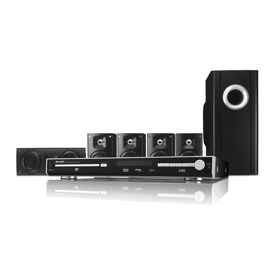
HOME THEATER WITH DVD HT-CN150DVW
SUPER WOOFER 5.1 SPEAKER SYSTEM
ON / STAND-BY
MP3
Specifications..................................................................................................................................................................2
Laser Beam Safety Precautions ..............................................................................................................................4
Important Safeguards And Precautions .............................................................................................................5
Standard Notes For Servicing .................................................................................................................................6
Operating Controls And Functions......................................................................................................................10
Troubleshooting ..........................................................................................................................................................13
Block DiagramS ..............................................................................................................................................................16
Schematic Diagrams / Ic's Pin Voltage ...................................................................................................................18
Waveforms .......................................................................................................................................................................40
Wiring Diagram ...............................................................................................................................................................42
System Control Timing Charts................................................................................................................................53
Ic Pin Function Descriptions ....................................................................................................................................54
Lead IdentificationS ....................................................................................................................................................100
Fl Display .........................................................................................................................................................................101
PART GUIDE
SHARP CORPORATION
SERVICE MANUAL
ON/STAND BY
OPEN/CLOSE
FUNCTION I/P SCAN
MUTE
SLEEP
MIC
KEY
ECHO
DISPLAY
DIRECT
ZOOM
PROG
EQ
LISTENING REPEAT
A-B
ADJ/VOL
TITLE
MENU/PBC
ENTER
SETUP
RETURN
PLAY/PAUSE
SLOW/
STOP
MEMORY
V
TUNING
V
PRESET
NTSC/PAL ST/MO
MODE
LANGUAGE
STEP
ANGLE SUBTITLE
AUDIO
9 2 L W I R 1 5 0 Z 0 4 D 7
OPEN /CLOSE
REMOTE
AUDIO/VIDEO
SENSOR
MIC VOLUME
FUNCTION
MODE
PLAY
STOP
SKIP
-
VOLUME
+
MIN.
MAX.
MIC
CONTENTS
Home Theater with DVD
HT-CN150DVW
MODEL
• In the interests of user-safety (Required by safety regula-
tions in some countries) the set should be restored to its
original condition and only parts identical to those specified
be used.
This document has been published to be used for
after sales service only.
The contents are subject to change without notice.
1
HT-CN150DVW
No. S7501HTN150DW
Page
Advertisement
Table of Contents

Related Manuals for Sharp HT-CN150DVW


Summary of Contents for Sharp HT-CN150DVW
- Page 1 NTSC/PAL ST/MO MODE LANGUAGE STEP ANGLE SUBTITLE AUDIO 9 2 L W I R 1 5 0 Z 0 4 D 7 HOME THEATER WITH DVD HT-CN150DVW SUPER WOOFER 5.1 SPEAKER SYSTEM ON / STAND-BY OPEN /CLOSE REMOTE AUDIO/VIDEO SENSOR...
-
Page 2: Specifications
Market SPECIFICATIONS As part of our policy of continuous improvement, SHARP reserves the right to make design and specification changes for product improvement without prior notice. The performance specification figures indicated are nominal values of pro- duction units. There may be some deviations from these values in individual units. -
Page 3: Front Speakers
HT-CN150DVW ● Front speakers Type Full range speaker system (magnetic shield) 8 cm (3-1/8") speaker Maximum input power 40 W Impedance 8 ohms Dimensions Width: 91.5 mm (3-5/8") Height: 139.5 mm (5-1/2") Depth: 100 mm (3-15/16") Weight 0.7 kg (1.5 lbs.)/each ●... -
Page 4: Laser Beam Safety Precautions
HT-CN150DVW LASER BEAM SAFETY PRECAUTIONS This DVD player uses a pickup that emits a laser beam. Do not look directly at the laser beam coming from the pickup or allow it to strike against your skin. The laser beam is emitted from the location shown in the figure. When checking the laser diode, be sure to keep your eyes at least 30cm away from the pickup lens when the diode is turned on. -
Page 5: Important Safeguards And Precautions
HT-CN150DVW IMPORTANT SAFEGUARDS AND PRECAUTIONS 1. IMPORTANT SERVICE NOTES BEFORE RETURNING THE DVD VIDEO PLAYER Reverse the AC plug on the set and repeat AC voltage measurements for each exposed part. Any reading of Before returning the DVD video player to the user, 1.4V rms (this corresponds to 0.7mA rms AC.) or more... -
Page 6: Standard Notes For Servicing
HT-CN150DVW STANDARD NOTES FOR SERVICING Circuit Board Indications Using lead-free wire solder a. The output pin of the 3 pin Regulator ICs is indicated When fixing the PWB soldered with the lead-free solder, as shown. apply lead-free wire solder. Repairing with conventional lead wire solder may cause damage or accident due to cracks. - Page 7 Soldering Iron Fig. S-1-3 (2) Lift each lead of the flat pack-IC upward one by one, using a sharp pin or wire to which solder will not adhere (iron wire). When heating the pins, use a fine Fig. S-1-1 tip soldering iron or a hot air desoldering machine.
- Page 8 HT-CN150DVW (4) Bottom of the flat pack-IC is fixed with glue to the 2. Installation CBA; when removing entire flat pack-IC, first apply (1) Using desoldering braid, remove the solder from the soldering iron to center of the flat pack-IC and heat foil of each pin of the flat pack-IC on the CBA so you up.
- Page 9 HT-CN150DVW Instructions for Handling Semi-conductors Electrostatic breakdown of the semi-conductors may occur due to a potential difference caused by electrostatic charge during unpacking or repair work. 1. Ground for Human Body Be sure to wear a grounding band (1MΩ) that is properly grounded to remove any static electricity that may be charged on the body.
-
Page 10: Operating Controls And Functions
HT-CN150DVW OPERATING CONTROLS AND FUNCTIONS ■ Main unit (front panel) HOME THEATER WITH DVD HT-CN150DVW ON / STAND-BY OPEN /CLOSE REMOTE SENSOR MIC VOLUME FUNCTION MODE PLAY STOP SKIP VOLUME MIN. MAX. 16 17 18 19 20 21 22 P-SCAN... - Page 11 HT-CN150DVW ■ Main unit (rear panel) AUDIO ANTENNA FRONT SURROUND Manufactured under license from Dolby Laboratories. DIGITAL INPUT CENTER WOOFER "Dolby", "Pro Logic" and the double-D symbol are trademarks of Dolby Laoratories. 127V COMPONENT AUDIO OUT VIDEO COAXIAL VIDEO OUT Manufactured under license from Digital Theater Systems, lnc.
-
Page 12: Remote Control
HT-CN150DVW ■ Remote Control Remote Control Transmitter On/Stand-by Button Function Button Direct Number Buttons Mic Button Sleep Button ON/STAND BY OPEN/CLOSE FUNCTION I/P SCAN Display Button Direct Button MUTE EQ (equalizer) Button 10. Surround/Stereo (2-ch) Listening Mode Button 11. Volume Up and Down or Speaker Level Adjust Buttons 12. -
Page 13: Troubleshooting
HT-CN150DVW TROUBLESHOOTING TROUBLESHOOTING CHART (1/3) - Page 14 HT-CN150DVW TROUBLESHOOTING CHART (2/3)
- Page 15 HT-CN150DVW NO DISC STATUS CD PLAY STATUS TROUBLESHOOTING CHART (3/3)
-
Page 16: Block Diagrams
HT-CN150DVW BLOCK DIAGRAM +12V -12V FM IN +6.8V POWER AM IN PCON SUPPLY TEA5762H+SAA6588T -24V 3.6V AC RADIO PACK AC input 120V/230V RESET +5V_STB FLASH SST39VF080 SDRAM TV-IN TV-IN 4MX16 IC TC4052B IC AT24C02 SERIAL EEPROM AUX-IN 27MHZ L CH... - Page 17 HT-CN150DVW SPDIF-IN IC 74HC04 SPDIF-OUT Y.V.U OUT S-VIDEO ES6629FD C-VIDEO SCART IO-PUT IC 74HC374 VFD(DR1060) IC 74HC374 IC HT16511 IO-PUT HT48R05 IC WM8772 LINE OUT PCON RC4558D D/A EXCHANGE IC EC6603 (RF) AT5660 (DRIVER) IC RC4558D IC RC4558D IC RC4558D...
-
Page 18: Schematic Diagrams / Ic's Pin Voltage
HT-CN150DVW SCHEMATIC DIAGRAMS / IC’S PIN VOLTAGE Standard Notes Notes: 1. Do not use the part number shown on these draw- WARNING ings for ordering. The correct part number is shown in the parts list, and may be slightly different or Many electrical and mechanical parts in this chassis amended since these drawings were prepared. - Page 19 HT-CN150DVW LIST OF CAUTION, NOTES, AND SYMBOLS USED IN THE SCHEMATIC DIAGRAMS ON THE FOLLOWING PAGES: 1. CAUTION: FOR CONTINUED PROTECTION AGAINST FIRE HAZARD, REPLACE ONLY WITH THE SAME TYPE FUSE. 2. CAUTION: Fixed Voltage (or Auto voltage selectable) power supply circuit is used in this unit.
- Page 20 HT-CN150DVW MAIN CIRCUIT DIAGRAM R323 47K IC301 TC4052B R324 47K R315 100K JK401-A X-COM R301 43K L301 100ohm C301 100P R316 100K C302 100P Y-COM L302 100ohm R302 43K R303 43K L303 100ohm C303 R319 C429 100P P+12V R320 R421...
- Page 21 HT-CN150DVW R401 4K7 R402 C403 R416 150P IC401-A C405 R403 C401 JRC4558d 10u/16V R431 C426 10u/16V C461 R417 C402 103(562) C463 C427 R418 10u/16V R432 68K R436 33K(56K) R437 4K7(330) R404 4K7 R405 C404 P-12V R419 R433 360K C408 150P...
- Page 22 HT-CN150DVW M62446-DATA Q301 M62446-CE 2SC945 D312 1N4148 C452 C451 C450 D313 1N4148 D314 1N4148(OPEN) D315 1N4148 VDDP R463 C497 10u/16V R967 R464 C474 C473 C482 C481 R470 100K Q404 2SA733(OPEN) C488563 CN903 FOR SWITCH POWER PCB C493 C494 C469 CN902 FOR SWITCH POWER PCB...
- Page 23 HT-CN150DVW CN401 R468 OPEN 12K(OPEN) VSSP VDDP C511 C508 47U/63V VDDP R563 R564 VSSP C512 R565 CLOCK MODE 2 C509 C513 R510 10 R566 MODE 3 C473 C514 C510 C501 IN1+ C503 330P IN1- IC501 C505 C505 OUT1 TDA8921TH SGND1...
- Page 24 HT-CN150DVW SERVO CIRCUIT DIAGRAM DVD LOADER (AMTEK) CN801 TRACK- IC802 20PIN TRACK- TRACK+ IC802 15PIN TRACK+ FOCUS- IC802 5PIN FOCUS+ IC802 14PIN DVDPD IC801 23P RF50V VCC5V Q806 2SB1132 2.1V 4.6V DVDLD CDLD L802 CDPD IC801 24P 3.9V VCD/CD DVDRF C816-IC801 1#...
- Page 25 HT-CN150DVW C818 820P(104) C817 C821 C819 C820 C823 C824 470P R806 Q806 2SB1132 2.1V RF33V 4.6V L802 C816 472 SCSJ DVDFRP SDEN C815 SDATA 680P(OPEN) DVDRFN SDATA 3.9V VCD/CD SCLK SCLK C814 C813 680P C826 2SB1132 Q805 C812 C811 1.8V 4.5V...
- Page 26 HT-CN150DVW R847 R845 R846 C821 1M(OPEN) RF50V 10M(OPEN) SPDIF-OUT C823 C824 470P IC803-E IC803-D 74HCO4 74HCO4 IC803(OPEN) R806 RF33V IC803-C IC803-F 74HCO4 74HCO4 C825 SPDIF-IN R848 100(OPEN) SCSJ SDEN SDATA SDATA IC803-B IC803-A SCLK 74HCO4 SCLK 74HCO4 C826 R849 10K(OPEN)
- Page 27 HT-CN150DVW R847 R846 JK801 1M(OPEN) OPEN 10M(OPEN) L804 L809 Y/U/V C845 C844 IC803-D 470P 470P 74HCO4 L810 L811 IC803-C L805 1uH 74HCO4 C847 C846 470P 470P JK802-A IC803-B 74HCO4 L806 1uH L812 1uH L813 1uH(OPEN) VOUT L807 CN804 C851 C850...
- Page 28 HT-CN150DVW TRACK TRACK- MICL MICR TP36 R815 1K CLOSE(189PIN) TP35 CLOSE TP34 R270 4.7K RF33V TP33 R816 OPEN(191PIN) CN803 RB803 SW803 TRAY-SW1 R817 CLOSE SW CLOSEW(187PIN) LM358 SW804 IC805-A TRAY-SW2 OPEN SW 3.3V DCLOAD- OPENSW(190PIN) R818 DCLOAD+ R812 R811 Q201...
- Page 29 HT-CN150DVW R209 OPEN MVCC (189PIN) C220 R210 R270 4.7K RF33V 191PIN) C222 C873 W(187PIN) LM358 3.3V IC805-A 3.3V LM358 W(190PIN) 3.3V IC805-B R812 R811 R213 R215 15K(0) C232 C259 R221 TUN_B+/SW R249 MUTE C260 FERQ_HOP R250 TUN-CLK R223 TUN-CE R251...
- Page 30 HT-CN150DVW OPEN OPEN R209 C219 OPEN C220 R210 C221 560P C222 AVSS-DS AVSS-PL XSPDOFTR1 XSFD0 XSFTR0PI R211 AVDD3-PL XSPLLFTR1 XSPLLFTR2 R212 XSERVF0 C226 XSAWRC AVSS_DA SVREF15 XSRFRPCTR XSTRAY AVDD3_DA R213 XSSPINDLE R214 XSFOCUS XSSLEGP R215 15K(0) XSSLEGN R216 XSTRACK XSTESTDA...
- Page 31 HT-CN150DVW C255 RBCK R243 VD33_PLL RWS/TDMFS R242 0 R241 OPEN RBCK/TDMCLK RSD/TDMDR LA16 VD33 LA15 VS33 LA14 LA20 LA13 LA19 A19/A-1 LA12 LA11 LOE# LWRLL LCS3# CLS3 RESET R240 OPEN LCS2# RDY/BUSY LCS2 LCS1# LA18 LCS1 LCS0 L0E# VD33 LCS3#...
- Page 32 HT-CN150DVW DISPLAY/STANDBY SCHEMATIC DIAGRAM P-SCAN DIGITAL AUDIO PROLOGICII SCAD DP201 STEREO C221A R241A C223A 100u/35 R245A 10K SG20/GR9 DOUT SG19/GR10 IC202A SG18/GR11 TP6311 SG17/GR12 SG16/GR13 SG15/GR14 GR15 GR16 R249A R250A R251A R252A D202 1N4148 D203 1N4148 D201 1N4148 R232A 100K...
- Page 33 HT-CN150DVW TITLE PRESET PROG SLEEP WAKEUP REPEAT1 P-SCAN DIGITAL AUDIO PROLOGICII SCAD STEREO C222A PLAY STBY PCON P-MUT -24V DGND PCON P-MUTE EN1(VOL-A) EN2(VOL-B) -24V V-DATA V-CLK V-CS RB201 Q204 2SC945 R222 R232A 100K R224A R228A 1.2K RB202A RB202B LD201...
- Page 34 HT-CN150DVW KARAOKE/MIC SCHEMATIC DIAGRAM -12V R808A R845A C805A 10K(OPEN) C810A C807A C811A 4.7UF/50V 10UF/25V IC803A C842A C812A R806A 10UF/25V R805A 200K R807A R813A R812A R811A R810A R809A C808A R814A C804A C806A 10UF/25V C813A C814A C815A C809A +C822A +12V 10UF/25V R819A...
- Page 35 HT-CN150DVW -12V JK801A IC803A RC4558D C802A L801A R803A 100UH 3.3K 1UF/50V C801A R801A R802A C803A 805A 200K C804A UF/25V R804A R823A R819A Q801A C826A D802A R820A R821A 2SC945 LL4148 10UF/25V +C827A R821A D801A R822A 100UF/16V LL4148 C825A 4.7UF/50V R824A R825A...
- Page 36 HT-CN150DVW TUNER CIRCUIT DIAGRAM CN12P-20 CN12P-20 CN001 100U C047 C048 104P 153P 220P C023 PSWO R039 C028 153P C022 220P C027 R038 152P C033 DAVN AFIN R034 VDDA VDDD R024 22OU 104P VSSA VSSD C010 2SC945 222P Q002 C043 D004...
- Page 37 HT-CN150DVW POWER SCHEMATIC DIAGRAM 835-1A-B-C T5H 250V LF-18-LP3018D 5 OHM RL 1 NTC1 250V 1KP FL 2 47K/3W 1/2W 470K CN 1 GBU4J CN 02 250V 1KP P6KE300A 300V 1/2W 1M SO222 1/2SL14 1/2W 220 250V/4.7KP 1/4W 1.5K 250V/4.7KP HZ12C2 TA 50V/0.1u...
- Page 38 HT-CN150DVW R245 -27V -27V CR 1.05mH CR243 L123 1KV/0.01u -27V 1/2W 1 STTH2003CT C242 C244 R243 C245 50V/1Ku 50V/100u 2W 2K 50V/0.1u C246 500V/470P C311 500V/220P 300A 300V BYM26E +27V FQA8N80 CR311 C312 C314 R251 C252 50V/1Ku 50V/100u 2W 2K 50V/0.1u...
- Page 39 HT-CN150DVW IC’S Pin Voltage IC802 AT5660, MOTOR DRIVER PIN NO. MODE STOP 1.5V 2.5V 2.5V 1.5V 2.5V 1.2V 1.2V 1.5V 6.1V 6.1V 2.5V 2.5V 2.5V 2.5V 3.6V 3.6V 5.0V 2.5V PLAY 1.5V 2.5V 2.5V 1.5V 2.5V 5.2V 5.6V 5.6V 5.6V 2.5V...
-
Page 40: Waveforms
HT-CN150DVW WAVEFORMS VIDEO OUT S-VIDEO OUT - Y Output Note : S-VIDEO OUT - C Output WF1 ~ WF3 : Power On (Stop) Mode. WF4 ~ WF7 : DVD Test Disc TDV-540A. (Color Bar 75%) COMPONENT VIDEO OUT - Y Output... - Page 41 HT-CN150DVW COMPONENT VIDEO OUT - Pr/Cr Output COMPONENT VIDEO OUT - Pr/Cr Output (Interlace mode) (P-Scan mode) WF10 Audio Left WF11 Audio Right WF12 Rf Signal Note : WF8 ~ WF9 : DVD Test Disc TDV-540A. (Color Bar 75% ) WF10 ~ WF11 : DVD/CD Test Disc 1KHz, 0dB.
-
Page 42: Wiring Diagram
HT-CN150DVW WIRING DIAGRAM MAIN PCB LAYOUT (TOP) From Karaoke MAIN PWB-A1 RB801A (CNS801) CN901 +6.V8 -27V +12V AC1 AC2 CN202 CN902 CN903 R957 R968 R261 ZD202 R260 C975 C973 C951 C952 C979 C5041 R951 R952 C586 C5065 R969 C579 IC953... - Page 43 HT-CN150DVW From Display CN201 From Tuner From Pick-Up CN001 FFC1 (CNS001) (CNS001) CN151 CN801 CN202 C2031 CN803 CN812 CN813 CN903 FB643 CN201 CN801B D316 FB509 R831 D308 FB644 R805 C973 C977 D306 D307 Q806 C979 D305 C835 C984 D314 D312...
- Page 44 HT-CN150DVW MAIN PCB LAYOUT (BOTTOM) R967 C594 C591 R549 IC505 C592 R550 C597 R5051 R554 C596 R553 Q5042 C5049 C5050 C7893 C5048 IC504 C599 Q5041 R5042 C7892 C5046 C5060 R5053 C569 C962 C565 R531 C563 R529 C564 R530 C566 R532...
- Page 45 HT-CN150DVW EN2L2 C5882 R967 FB504 EC21 RF08 IC208 EN2L1 EN1L2 FB508 C7884 C7885 R833 C7883 C828 C818 C873 R288 R289 C821 C810 EN2L3 C824 D5551 C802 C224 R212 C248 C247 C225 C230 R216 R231 C246 C7882 C252 C214 C001A C001B...
- Page 46 HT-CN150DVW CONTROL PCB LAYOUT (TOP) RB845B 3 2 1 TO CN845A C207A CN845A CN855A C810A RB801A E C B TO CN801A Q807A C217A RB201 TO CN855A 3 2 1 LD201 STANDBY PWB-B2 MIC PWB-B4 CONTROL PCB LAYOUT (TOP)
- Page 47 HT-CN150DVW CONTROL PCB LAYOUT (BOTTOM) 3 2 1 EMC2 R221A R222A C212A D9009 C206A R217A ZD201A C209A R214A R216A D9008 C202A C203A C204A C201A R219A R208A R207A R228A R213A R206A R215A R205A R212A R204A R211A R203A R202A R210A R209A R201A...
- Page 48 HT-CN150DVW TUNER PWB LAYOUT (TOP) TO MAIN CN151 (CNS001) CN001 CN001 C039 Q003 R031 C025 T003 C017 T004 C046 C037 C045 C029 R005 C008 T006 VD001 C004 T001 C005 T005 EF450-G1 L004 CN002 D001 D002 ANT001 TUNER PWB LAYOUT (TOP)
- Page 49 HT-CN150DVW TUNER PWB LAYOUT (BOTTOM) C069 C003 C070 C002 R037 R036 Q004 C031 R026 R017 Q001 R014 R012 EF450-G1 C050 C006 C032 C007 R006 VD001 T002 C012 C011 T003 R010 C022 Q002 C023 C041 R018 C034 R019 C013 IC002 R021...
- Page 50 HT-CN150DVW POWER PWB LAYOUT (TOP) POWER PWB LAYOUT (TOP)
- Page 51 HT-CN150DVW POWER PWB LAYOUT (BOTTOM) POWER PWB LAYOUT (BOTTOM)
- Page 52 HT-CN150DVW POWER PWB LAYOUT (COMPONENTS) WARNING: UTILISER UN FUSIBLE DE RECHANE DE MEME TYPE WARNING: FOR CONTINUED PROTECTION AGAINST RISK FIRE REPLACE WITH SAME TYPE T5H 250V R17 R16 R301 D271 D681 C319 R312 C126 C246 C130 C240 R314 R124...
-
Page 53: System Control Timing Charts
HT-CN150DVW SYSTEM CONTROL TIMING CHARTS Tray Close ~ Play / Play ~ Tray Open Tray Disc Play Tray Tray Close Rotation Stop Open Tray IN 3.3V (CN803 pin 1/ IC201 pin 187) Sled Drive 1.65V (IC802 Pin 12) Disc Drive 1.65V... -
Page 54: Ic Pin Function Descriptions
HT-CN150DVW IC PIN FUNCTION DESCRIPTIONS IC401, DUAL WIDE BANDWIDTH OPERATIONAL AMPLIFIERS (RC4558) Pin Configuration: Pin Description: Function Pin No. Output A Input A Input A Input B Input B Output B IC301,4 CHANNEL MULTIPLEXER (D4052) Pin Configuration: IN/OUT IN/OUT OUT/IN... - Page 55 HT-CN150DVW IC805,DUAL OPERATIONAL AMPLIFIERS (LM358MX) Pin Configuration: Block Diagram: OUTPUT A 1OUT 1IN- 2OUT INVERTING INPUT A OUTPUT B 1IN+ 2IN- 2IN+ NON-INVERTIN G INVERTING INPUT B INPUT A NON-INVERTING INPUT B Symbol (each amplifier) IC501,DUAL D-TYPE FLIP-FLOP (CD4013BT/HEF4013BT) Block Diagram:...
- Page 56 HT-CN150DVW IC301, 4 CHANNEL MULTIPLEXER (D4052BM) Pin Configuration: IN/OUT IN/OUT OUT/IN D4052BM OUT/IN IN/OUT IN/OUT TOP VIEW Block Diagram: X CHANNELS IN/OUT COMMON X OUT/IN COMMON Y OUT/IN SINARY LOGIC 1 OF 4 LEVEL DECODER CONVERSION WITH INHIBIT Y CHANNELS IN/OUT...
- Page 57 HT-CN150DVW IC504, CMOS Hex Inverter IC (74HCU040D) Pin Configuration: V cc Top View Schematic Diagram: V cc...
- Page 58 HT-CN150DVW IC208, 1A Fixed & Adj Low Dropout Positive Voltage Regulators (RT9164-33CLR) Pin Configuration: Pin No. Name ADJ/GND Vout Pin Description: Pin Name Pin Function ADJ/GND Adjust or Ground VOUT Output Positive Power Input Block Diagram: S.O.A CURRENT LIMIT LIMITING...
- Page 59 HT-CN150DVW IC801A, Echo Processor IC (PT2399) Block Diagram: LPF1 - IN LPF1 - OUT LPF2 - OUT LPF2 - IN OP2-OUT OP2-IN OP2-IN OP1-OUT 4.7K 4.7K LPF2 COMP LPF 1 1/2 Vcc CLOCK AUTO RESET 44K Bits AGND DGND CLK_0...
- Page 60 HT-CN150DVW Echo Processor IC (PT2399) Pin Description: Pin Name Description Pin No. Analog Supply Voltage Input Analog Reference Voltage (=1/2VCC) AGND Anolog Ground DGND Digital Ground CLK_0 System Clock Output Pin Frequency Adjustment Pin Current Contol 1 Current Contol 0...
- Page 61 HT-CN150DVW IC204, Micropower Supply Voltage Supervisor (CM3403) Pin Description: RESET 3-pin SOT23 Pin Description: PIN(S) NAME DESCRIPTION Negative reference for all signals. RESET Active low reset output. When the sence threshold has been exceeded, the RESET signal will remain active for an additional 140(min.) after which it is taken inactive. During a "brownout" condition, RESET will immediately be taken active.
- Page 62 HT-CN150DVW IC802, 5-Channel Motor Driver for DVD/VCD (AT5660) Pin Description: PGND AT5660 PGND Pin Description: PIN NO. Pin name Function CH1 (Focus coil) input CAP1_1 CH1 error amplifier filter capacitor connection 1 CAP1_2 CH1 error amplifier filter capacitor connection 2...
- Page 63 HT-CN150DVW IC802, 5-Channel Motor Driver for DVD/VCD (AT5660) Block Diagram: STAND- MUTE 1_2_3_4 7.5K CAP1_1 VBIAS IN4- CAP_2 CAP4_1 7.5VK 7.5K CAP4_2 7.5K PGND PGND VCC1 Pre-DRV VCTL VCC1 OUT5- TRAY DRIVER VCC2 OUT5+ VCC2 OUT3- OUT2- VCC1 VCC1 SLED...
- Page 64 HT-CN150DVW IC202A, VFD Driver (PT6311) Pin Description: Pin Name Function Pin No. SW1 to SW4 General Purpose Input Pins 1 to 4 Data Output Pin (N-Channel, Open-Drain) This Pin outputs serial data at the falling DOUT edge of the shift clock (starting from the lower bit )
- Page 65 HT-CN150DVW IC202A, VFD Driver (PT6311) Block Diagram: SG1/KS1 SG2/KS2 Control SG3/KS3 SG4/KS4 Serial SG5/KS5 DOUT Data SG6/KS6 Interface Display Memory SG7/KS7 (20 bits X 16 works) Segment SG8/KS8 Driver/ SG9/KS9 Grid SG10/KS10 Driver/ SG11/KS11 Key Scan/ SG12/KS12 Timing Generator Output...
- Page 66 HT-CN150DVW IC 202A, VFD Driver (PT6311) Pin Configuration: 41 40 SG20/GR9 SG19/GR10 DOUT SG18/GR11 SG17/GR12 SG16/GR13 SG15/GR14 SG14/GR15 SG13/GR16...
- Page 67 HT-CN150DVW IC801, ESS DVD SERVO (ES6603S) Pin Configuration: IC801, ESS DVD SERVO (ES6603S) 47 46 3 5 3 4 MEVO MLPF 47 46 3 5 3 4 MEVO MIRR LDON MLPF ES6603S RFAC CDPD DVDPD MIRR CDLD LDON DVDLD ATON...
- Page 68 HT-CN150DVW IC801, ESS DVD SERVO (ES6603S) Pin Description: Table 1 lists the pin descriptions for the ES6603. The pound symbol (#) iindicates an active-low signal. Table 1 ES6603 Pin Descriptions List Name Pin Numbers Definition DVDRFP, Differential RF signal attenuator inputs.
- Page 69 HT-CN150DVW Name Pin Numbers Definition RFDC bottom envelope. Connected to VPA pin 58 via a capacitor. RF block and serial port ground. Differential outputs of equalizer/filter. FNN, FNP 52, 53 Differential analog inputs to the RF single-end output buffer and full wave rectifier.
- Page 70 HT-CN150DVW Name Pin Numbers Definition 1, 2 Differential RF signal attenuator inputs [DVDRFP] and [DVDRFN]. 52, 53 Differential normal filter outputs [FNP] and [FNN]. 54, 55 Differential analog RF buffr inputs [DIP] and [DIN]. AGC and Filter Interface Single-ended RF output [RFAC].
- Page 71 HT-CN150DVW IC201, ESS VIBRATTO-ll DVD Processor (ES6629) Pin Configuration: AVSS_DS VD33_PL AVSS_PL PDOFTR1 RBCK FTROPI AVDD3_PL PLLFTR1 PLLFTR2 VREF0 VD33 AWRC VS33 AVSS_DA RFRPCTR TRAY AVDD3_DA SPINDLE LOE# FOCUS LWRLL# SLEGP LCS3# SLEGN TRACK TESTDA LCS2# FGIN LCS1# LCS0# PHOI...
- Page 72 HT-CN150DVW Table 1 ES6629 Pin Description Name Pin Numbers Definition VD33 1,10,19,35,44,53,62,79,96,126,185 I/O power supply. VID_XI Crystal input. VID_XO Crystal output. System clock. DMA [11:0] 5:8 11:17, 20 DRAM address bus. VS33 9,18,34,43,52,61,78,95,119,127,186,208 Ground for I/O power supply. DCAS# DRAM column address strobe (active-low).
- Page 73 HT-CN150DVW Name Pin Numbers Definition UDAC Video DAC ouput Value F DAC V DAC Y DAC C DAC U DAC CVBS/Chroma CVBS1 CVBS/Chroma CVBS1 CVBS2 CVBS/Chroma CVBS/Chroma CVBS1 CVBS2 CVBS/Chroma CVBS1 CVBS/Chroma CVBS1 CVBS/Chroma SYNC CVBS/Chroma Chroma CVBS CVBS1 CVBS...
- Page 74 HT-CN150DVW Name Pin Numbers Definition SPDIF_IN S/PDIF input; (5V tolerant input). WBLCLK DVD-RAM wobble detector circuit clock source to preamp. DVD-RAM wobble output. DVD-RAM land/groove flag. DVD-RAM header position index 2. DVD-RAM header position index 1. FLAG[3:0] 133: 136 To monitor servo status.
- Page 75 HT-CN150DVW Name Pin Numbers Definition TESTDA Test DA output. FGIN Spindle hall sensor input. PHOI Sledge photo interrupt signal input. SCSJ Chip selection signal to RF chip (serial data enable). SDATA Data signal from/to RF chip. SCLK Serial clock source to RF chip.
- Page 76 HT-CN150DVW Name Pin Numbers Definition LOE# RISC port output enable (active-low). LD[7:0] 91:94, 97;100 RISC port data bus; (5V tolerant input). Audio receive serial data; (5V tolerant input). RBCK Audio receive bit clock; (5V tolerant input). Audio receive frame sync; (5V tolerant Input).
- Page 77 HT-CN150DVW ES6629 DEVICE INTERFACES Table 2 lists the devices interfaces for the ES6629. Table 2 ES6629 Device Interfaces Name Pin Numbers Definition Audio receive serial data input [RSD]; (5V tolerant input). Audio receive bit clock input [RBCK]; (5V tolerant input).
- Page 78 HT-CN150DVW Name Pin Numbers Definition Power and Ground Analog ground for ADC [AVSS_AD]. Analog power supply for data slicer [AVDD3_DS]. Analog ground for data slicer [AVSS_DS]. Analog ground for data PLL [AVSS_PL]. Analog power supply for data PLL [AVDD3_PL]. Analog ground for DAC [AVSS_DA].
- Page 79 HT-CN150DVW Name Pin Numbers Definition 133:136 To monitor servo status [FLAG(3:0)]. Spindle hall Sensor input [FGIN]. Sledge photo interrupt signal input [PHOI]. Chip selection signal to RF chip (serial data enable) [SCSJ]. Data signal from/to RF chip [SDATA]. Servo Control and Data Serial clock source to RF chip [SCLK].
- Page 80 HT-CN150DVW IC201, ESS VIBRATTO-ll DVD Processor (ES6629) System Block Diagram: A sample system block diagram for the ES6629 Vibratto-ll DVD player board design is shown in Figure 2. DVD/CD Motor Motor Driver ES6603 Video TV DISPLAY RF AMP Audio DAC...
- Page 81 HT-CN150DVW IC351, 24bit 192KHz 6-Channel Codec with Volume Control (WM8772) Pin Description: Name Type Description MODE Digital input Control format selection 0=Solfware control 1=Hardware control MCLK Digital Input Master clock; 256,384, 512 or 768ls (fs=word clock frequency) BCLK Digital input/output...
- Page 82 HT-CN150DVW IC351, 24bit 192KHz 6-Channel Codec with Volume Control (WM8772) Block Diagram: VREFN VREFP VOUT1L STEREO PASS VOUT1R FILTER VREFN AUDIO AINL VOUT2L INTERFACE STEREO STEREO PASS & AINR VOUT2R FILTER DIGITAL FILTERS VOUT3L STEREO PASS VOUT3R FILTER CONTROL INTERFACE...
- Page 83 HT-CN150DVW IC501/IC502/IC503 2X50 W class-D power amplifier (TDA8921) Pin Description: Pin Configuration: Symbol Description negative analog supply voltage for channel 2 SSA2 SGND2 signal ground channel 2 positive analog supply voltage for channel 2 DDA2 IN2- negative audio input for channel 2...
- Page 84 HT-CN150DVW IC501/IC502/IC503 2X50 W class-D power amplifier (TDA8921) Block Diagram: FIGURE 1 BLOCK DIAGRAM...
- Page 85 HT-CN150DVW IC405, 6 Channel Volume Tone Control IC (M62446FP) PIN CONFIGURATION AND IC INTERNAL BLOCK DIAGRAM: OUT4 DVDD OUT- OUT3 PORT DATA OUT2 Volume LATCH OUT1 DGND AVDD Volume AGND SWin SW out GNDS SRout SRin Volume SLin SLout Cout...
- Page 86 HT-CN150DVW IC203, 4 Banks x IM x 16 Bit Synchronous DRAM (HY57V641620G) Pin Configuration: DQ15 VDDQ VSSQ DQ14 DQ13 VSSQ VDDQ DQ12 DQ11 VDDQ VSSQ DQ10 54pin TSOP II VSSQ VDDQ 400ml x 875ml 0.8mm pin pitch LDQM UDQM /CAS...
- Page 87 HT-CN150DVW IC203, 4 Banks x IM x 16 Bit Synchronous DRAM (HY57V641620G) Functional Block Diagram: Self refresh logic Internal Row & timer counter 1Mx16 Bank 3 1Mx16 Bank 2 Row active Decoders 1Mx16 Bank 1 1Mx16 Bank 0 Memory refresh...
- Page 88 HT-CN150DVW IC001, Self Tuned Radio (STR) (TEA5762) Block Diagram:...
- Page 89 HT-CN150DVW IC001, Self Tuned Radio (STR) (TEA5762) Pin Description: Symbol Description RIPPLE ripple capacitor input AM-RFI AMRF input RFGND RF ground and substrate CGND counter ground COUNTI counter input AMOSC parallel tuned AM-oscillator circuit to ground Vcc1 supply voltage TUNE...
- Page 90 HT-CN150DVW IC001, Self Tuned Radio (STR) (TEA5762) Pin Configuration: RIPPLE FM-IFI2 AM-RFI RFGND CGND COUNTI WRITE-ENABLE TEA5762H AMOSC DATA V CC1 BUS-CLOCK TUNE DGND XTAL MO/ST MPXI V DDD MBE 820...
- Page 91 HT-CN150DVW IC209, 800mA LOW DROPOUT POSITIVE FIXED 1.8V REGULATOR (IRU1117-18) Pin Configuration: IRU1117-18 Vout Pin Descriptions: Pin# Pin Symbol Pin Description Ground pin. This pin must be connected to ground plane using a low inductance short connection. Vout The output of the regulator. This pin is also connected to the tab of the package. An output capacitor must be connected to this pin to insure stability of the regulator.
- Page 92 HT-CN150DVW IC209, 800mA LOW DROPOUT POSITIVE FIXED 1.8V REGULATOR (IRU1117-33) Pin Configuration: IRU1117-18 IRU1117-33 Vout Vout Pin Descriptions: Pin# Pin Symbol Pin Description Ground pin. This pin must be connected to ground plane using a low inductance short connection. The output of the regulator. This pin is also connected to the tab of the package. An output capacitor Vout must be connected to this pin to insure stability of the regulator.
- Page 93 HT-CN150DVW IC202, 8m-BIT HIGH SPEED FLASH memory (mx 26LV800T/B) Pin Configuration: 48 TSOP (Standard Type) (12mm X 20mm) BYTE# Q15/A-1 RESET# MX26LV800T/B RY/BY# Pin Descriptions: SYMBOL PIN NAME A0-A18 Address Input Q0-Q14 Data Input/Output Q15/A-1 Q15(Word mode)/LSB add(Byte mode) Chip Enable Input...
- Page 94 HT-CN150DVW IC202, 8m-BIT HIGH SPEED FLASH MEMORY Block Diagram: WRITE CONTROL PROGRAM/ERASE STATE INPUT HIGH VOLTAGE MACHINE LOGIC RESET# (WSM) STATE MX26LV800T/B REGISTER FLASH ADDRESS ARRAY LATCH ARRAY SOURCE A0-A18 COMMAND Y-PASS DATA BUFFER GATE DECODER SENSE COMMAND DATA AMPLIFIER...
- Page 95 HT-CN150DVW IC206/IC207 Octal D-TYPE Flip-Flop with 3-STATE Outputs (74F374) Pin Configuration: Logic Symbols Connection Diagram...
- Page 96 HT-CN150DVW IC206/IC207 Octal D-TYPE Flip-Flop with 3-STATE Outputs (74F374) Pin Description: Input I U.L. Description Pin Names Output I HIGH/LOW 20 µ A/-0.6 mA –D Data Inputs 1.0/1.0 20 µ A/-0.6 mA Clock Pulse Input (Active Rising Edge) 1.0/1.0 20 µ A/-0.6 mA 3-STATE Output Enable Input (Active LOW) 1.0/1.0...
- Page 97 HT-CN150DVW IC205, SERIAL 2K (256x8) EEPROM (SSC24A02/m24(02) Pin Configuration: V CC MODE/WC V CC V SS E0-E2 m24C02 Signal Names: SSC24A02 E0-E2 Chip Enable Inputs MODE/WC* Serial Data Address Input/Output Serial Clock Multibyte/Page Write Mode V SS MODE (C version)
- Page 98 HT-CN150DVW IC201A, 8-BIT OTP microcontroller (HT48R05A-1) Block Diagram: Interrupt Circuit Prescaler FSYS STACK0 STACK1 TMR/PC1 Program Program INTC Counter TMRC SYS CLK/4 Instruction Register ı WDTS DATA Memory WDT Prescaler RC OSC PORT C PC0 - PC1 Instruction Decoder BZ/BZ...
- Page 99 HT-CN150DVW IC201A, 8-BIT OTP microcontroller (HT48R05A-1) Pin Description: ROM Code Pin No Pin Name Description Option Bidirectional 8-bit input/output port. Each bit can be configured as wake-up input by ROM 4~1, Pull-high* PA0~PA7 code option.Software instructions determine the CMOS output or schmitt trigger input with...
-
Page 100: Lead Identifications
HT-CN150DVW LEAD IDENTIFICATION Q1, 800V N-Channel MOSFET (FQA8N80) Anode Collector Emitter Cathode IC9550, Voltage Regulator (L7912) IC2, Photo Coupler (SFH617A) CR121, Ultra Fast Recovery Rectifier Diode ( STPR1020CT) CR681, High Voltage Power Schottky Rectifier (STPS20H100CT) -
Page 101: Fl Display
HT-CN150DVW FL DISPLAY GRID ASSIGNMENT... - Page 102 HT-CN150DVW ANODE CONNECTION...
-
Page 103: Parts Guide
HT-CN150DVW PARTS GUIDE Home Theater with DVD HT-CN150DVW MODEL CONTENTS [1] INTERGRATED CIRCUITS [12] ARRAY PARTS [2] TRANSISTORS [13] OTHER CIRCUITRY PARTS [3] DIODES [14] P.W.B. ASSEMBLY (Replacement Items) [4] FILTERS CABINET PARTS (MAIN UNIT) [5] VIBRATORS/CRYSTAL ACCESSORIES PARTS [6] RESONATOR... - Page 104 HT-CN150DVW PRICE PART PARTS CODE DESCRIPTION RANK MARK RANK [1] INTERGRATED CIRCUITS IC001 92LRCI57620001 IC 44pin TEA5762H, Self Tuned Radio(STR) IC IC201 92LRCI66291001 IC 208pin ES6629FDF ESS W/DTS, Vibratto-II DVD Processor IC201A 92LRCI48051Z01 IC 18pin HT48R05A-1 HOLTEK, 8bit Cost-effective 92LRCI26081001 (Asean except...
- Page 105 HT-CN150DVW PRICE PART PARTS CODE DESCRIPTION RANK MARK RANK [3] DIODES D801A 92LRCD11414810 Chip Diode, BAV16W / IN4148W D802A 92LRCD11414810 Chip Diode, BAV16W / IN4148W D803A 92LRCD11414810 Chip Diode, BAV16W / IN4148W D804A 92LRCD11414810 Chip Diode, BAV16W / IN4148W D951...
- Page 106 HT-CN150DVW PRICE PART PARTS CODE DESCRIPTION RANK MARK RANK [8] COILS L207 92LSCB06039601 Chip Bead, 60Ω 100MHz (0603 SMT Type) L208 92LSCN13361090 Chip Inductor, 1uH (0805 SMT Type) L301~L306 92LSCB80501010 Chip Bead, 100Ω 100MHz (0805 SMT Type) L351 92LSCN13361090 Chip Inductor, 1uH (0805 SMT Type)
- Page 107 HT-CN150DVW PRICE PART PARTS CODE DESCRIPTION RANK MARK RANK [10] CAPACITORS C217A 92LPVE83954101 Electrolytic Capacitor, 100uF 16V 20% C218A~C220A 92LPXL41037015 Chip Capacitor, 15pF 50V (0603 type NPO) C221 92LPXL05647473 Chip Capacitor, 0.047uF 50V (0603 Type X7R) C221A 92LPXL41037102 Chip Capacitor, 1000pF 50V (0603 type NPO)
- Page 108 HT-CN150DVW PRICE PART PARTS CODE DESCRIPTION RANK MARK RANK [10] CAPACITORS C425 92LPRE39570001 Electrolytic Capacitor, 10uF 50V 20% C426 92LPME03954010 Electrolytic Capacitor, 10 uF 16V 20% C427 92LPXL45647103 Chip Capacitor, 0.01uF 50V (0603 Type X7R) C428 92LPXL41037151 Chip Capacitor, 150pF 50V (0603 Type NPO)
- Page 109 HT-CN150DVW PRICE PART PARTS CODE DESCRIPTION RANK MARK RANK [10] CAPACITORS C595 92LPYL45647153 Chip Capacitor, 0.015uF 50V (0805 Type X7R) C596,C597 92LPYL41037561 Chip Capacitor, 560pF 100V ( 0805 Type NPO) C598 92LPRM373A0103 Mylar Capacitor, 0.01uF 100V 5% C599 92LPZL43967224 Chip Capacitor, 0.22uF 50V (1206 Type Y5V)
- Page 110 HT-CN150DVW PRICE PART PARTS CODE DESCRIPTION RANK MARK RANK [10] CAPACITORS C965 92LPRE39550221 Electrolytic Capacitor, 220uF 25V C966~C967 92LPRE39540221 Electrolytic Capacitor, 220uF 16V 20% C969 92LPYL43957104 Chip Capacitor, 0.1uF (0805 Type Y5V) C970,C971 92LPRE99550101 Electrolytic Capacitor, 100uF 25V 20% C973...
- Page 111 HT-CN150DVW PRICE PART PARTS CODE DESCRIPTION RANK MARK RANK [11] RESISTOR R002 92LQCF16503222 Chip Resistor, 2.2KΩ 1/16W (0603 SMT Type) R003 92LQCF16503100 Chip Resistor, 10Ω 1/16W (0603 SMT Type) R004 92LQCF16503221 Chip Resistor, 220Ω 1/16W (0603 SMT Type) R005 92LQCF16503471 Chip Resistor, 470Ω...
- Page 112 HT-CN150DVW PRICE PART PARTS CODE DESCRIPTION RANK MARK RANK [11] RESISTOR R252A 92LQCF16503103 Chip Resistor, 10KΩ 1/16W (0603 SMT Type) R253A 92LQCF16503472 Chip Resistor, 4.7KΩ 1/16W (0603 SMT Type) R254A 92LQCF16503103 Chip Resistor, 10KΩ 1/16W (0603 SMT Type) R255 92LQCF16503390 Chip Resistor, 360KΩ...
- Page 113 HT-CN150DVW PRICE PART PARTS CODE DESCRIPTION RANK MARK RANK [11] RESISTOR R505,R506 92LQCF01502562 Chip Resistor, 5.6KΩ 1/10W (0805 SMT Type) R510,R511 92LQCF06503010 Chip Resistor, 10Ω 1/16W (0603 SMT Type) R513~R516 92LQCF04501519 Chip Resistor, 5.1Ω 1/4W (1206 SMT Type) R517,R518 92LQCF02521220 Chip Resistor, 22Ω...
- Page 114 HT-CN150DVW PRICE PART PARTS CODE DESCRIPTION RANK MARK RANK [11] RESISTOR R833A 92LQCF16503223 Chip Resistor, 22KΩ 1/16W (0603 SMT Type) R834A,835A 92LQCF16503102 Chip Resistor, 1KΩ 1/16W (0603 SMT Type) R836 92LQCF16503000 Chip Resistor, 0Ω Jumper Wire (0603 SMT Type) R836A 92LQCF06503822 Chip Resistor, 8.2KΩ...
- Page 115 HT-CN150DVW PRICE PART PARTS CODE DESCRIPTION RANK MARK RANK [13] OTHER CIRCUITRY PARTS CN151 92LCCN20000108 8pin Connector, Pitch = 2.0mm CN201 92LCCN20000109 9pin Connector, Pitch = 2.0mm CN202 92LCCN20000105 5pin Connector, Pitch = 2.0mm CN801 92LCHC50050824 24pin Chip Connector, Pitch = 0.5mm, 90'...
- Page 116 HT-CN150DVW PRICE PART PARTS CODE DESCRIPTION RANK MARK RANK CABINET PARTS (MAIN UNIT) 92LGAL30170001 DVD BADGE 92LBPD01010843 TRAY COVER 92LASL26070003 DVD LOADER HR-M02-A 92LIVS01101001 DUST SHEET 92LBFP01210621 SPACER A 92LGSE14570101 MAIN CHASSIC 92LBRB00000493 LEG CUSHION 92LDSS10220001 SNAP LOCK 92LGSE14580001 SUPPORT ANGLE...
- Page 117 HT-CN150DVW PRICE PART PARTS CODE DESCRIPTION RANK MARK RANK FRONT SPEAKER BOX PARTS (CP-CN150F) 92LNSR54052B81 SCREW 92LBPQ500750AB REAR CABINET 92LBPH50003001 STOPPER 92LNST54082812 SCREW 92LYLB51158341 SPEC LABEL-LEFT 92LYLB51158415 SPEC LABEL-RIGHT 92LCJS50210502 JACK-LEFT (WHITE/BLACK) 92LCJS50210515 JACK-RIGHT(RED/BLACK) SP 1,2 92LFSA51330382 SPEAKER (MAGNECTIC SHIELD)
-
Page 118: Exploded View
HT-CN150DVW EXPLODED VIEW MAIN UNIT 619X6 HT-CN150DVW 619X2 617X5 618X3 PWB B-3 PWB B-1 616X2 619X2 DP201 PWB B-2 VR801A PWB B-4 613X3 608X10 609X4 611X2 610X2 612X2 PWB A-2 PWB A-1 607X6 601x4 606x2 602x4 TUNER 605x2 PACK 205x2... - Page 119 HT-CN150DVW FRONT SPEAKER CP-CN150F TERMINAL SPEAKER TERMINAL 904x4 SP1,2 907x4 Figure FRONT SPEAKER BOX PARTS...
- Page 120 HT-CN150DVW SURROUND SPEAKER CP-CN150R TERMINAL SPEAKER TERMINAL 904x4 907x4 SP1,2 Figure SURROUND BOX PARTS...
- Page 121 HT-CN150DVW CENTER SPEAKER CP-CN150C TERMINAL SPEAKER TERMINAL 904x4 908x4 Figure CENTER SPEAKER BOX PARTS...
- Page 122 HT-CN150DVW SUBWOOFER CP-CN150SW VOILET BLACK TERMINAL SPEAKER TERMINAL VOILET 906x4 BLACK Figure SUBWOOFER BOX PARTS...
- Page 123 HT-CN150DVW © COPYRIGHT 2004 BY SHARP CORPORATION ALL RIGHTS RESERVED. No part of this publication may be reproduced, stored in a retrieval system, or transmitted in any form or by any means, electronic, mechanical, photocopying, recording, or otherwise, without prior written permission of the publisher.