Table of Contents
Advertisement
Quick Links
Download this manual
See also:
Instruction Manual
SERVICE MANUAL
8
YD016
2004
TV
DVD
STANDBY/ON
OPEN
/CLOSE
TV
DVD
TV1
TV2
TV3
1
2
3
TV4
TV5
TV6
4
5
6
TV7
TV8
TV9
7
8
9
TV-/--
TV0
MUTING
10
0
+10
TITLE
TV/VIDEO
RETURN
PAGE
/GROUP
CANCEL
CH+
VOL
VOL+
ENTER
CH
PREVIOUS
NEXT
CLEAR
SELECT
SLOW-
SLOW+
3D PHONIC
ZOOM
VFP
PROGRESSIVE
SCAN
ANGLE
SUB TITLE
AUDIO
fs/Rate
AMP
VOL
REPEAT
DIMMER
1
PRECAUTION. . . . . . . . . . . . . . . . . . . . . . . . . . . . . . . . . . . . . . . . . . . . . . . . . . . . . . . . . . . . . . . . . . . . . . . . . 1-3
2
SPECIFIC SERVICE INSTRUCTIONS . . . . . . . . . . . . . . . . . . . . . . . . . . . . . . . . . . . . . . . . . . . . . . . . . . . . . . 1-6
3
DISASSEMBLY . . . . . . . . . . . . . . . . . . . . . . . . . . . . . . . . . . . . . . . . . . . . . . . . . . . . . . . . . . . . . . . . . . . . . . . 1-7
4
ADJUSTMENT . . . . . . . . . . . . . . . . . . . . . . . . . . . . . . . . . . . . . . . . . . . . . . . . . . . . . . . . . . . . . . . . . . . . . . . 1-15
5
TROUBLESHOOTING . . . . . . . . . . . . . . . . . . . . . . . . . . . . . . . . . . . . . . . . . . . . . . . . . . . . . . . . . . . . . . . . . 1-22
XV-N510B,XV-N512S
XV-N510BJC, XV-N510BCC, XV-N512SJC, XV-N512SCC
TABLE OF CONTENTS
COPYRIGHT © 2004 Victor Company of Japan, Limited
C --------------------- Canada
No.YD016
2004/8
Advertisement
Table of Contents

Related Manuals for JVC XV-N510B


Summary of Contents for JVC XV-N510B
-
Page 1: Table Of Contents
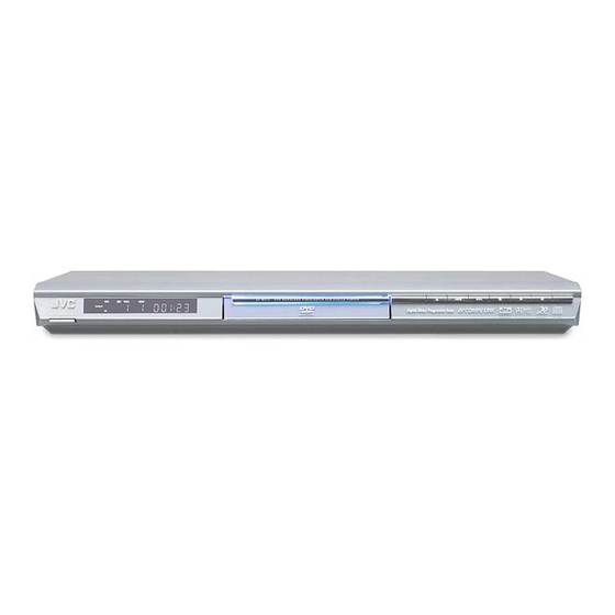
SERVICE MANUAL DVD AUDIO/VIDEO PLAYER YD016 2004 XV-N510B,XV-N512S Area Suffix J ------------------------ U.S.A. C --------------------- Canada STANDBY/ON OPEN /CLOSE TV-/-- MUTING TITLE TV/VIDEO RETURN PAGE /GROUP CANCEL VOL+ ENTER PREVIOUS NEXT CLEAR SELECT SLOW- SLOW+ 3D PHONIC ZOOM PROGRESSIVE SCAN... - Page 2 SPECIFICATION XV-N510B,XV-N512S for J,C General Readable discs DVD AUDIO, DVD VIDEO, DVD-R (Video format), DVD-RW (Video format/VR format), DVD-RAM (VR format), SVCD, Video CD, Audio CD (CD-DA), CD-R/RW (CD-DA, SVCD, Video CD, MP3/WMA format, JPEG) Video format REMOTE, 480i (Interlaced scan)/480p (Progressive scan) selectable...
-
Page 3: Precaution
SECTION 1 PRECAUTION Safety Precautions (1) This design of this product contains special hardware and path to the chassis, and measure the AC voltage across many circuits and components specially for safety purpos- the resistor. Now, reverse the plug in the AC outlet and es. - Page 4 Preventing static electricity Electrostatic discharge (ESD), which occurs when static electricity stored in the body, fabric, etc. is discharged, can destroy the laser diode in the traverse unit (optical pickup). Take care to prevent this when performing repairs. 1.5.1 Grounding to prevent damage by static electricity Static electricity in the work area can destroy the optical pickup (laser diode) in devices such as DVD players.
- Page 5 Precautions for Service 1.7.1 Handling of Traverse Unit and Laser Pickup (1) Do not touch any peripheral element of the pickup or the actuator. (2) The traverse unit and the pickup are precision devices and therefore must not be subjected to strong shock. (3) Do not use a tester to examine the laser diode.
-
Page 6: Specific Service Instructions
SECTION 2 SPECIFIC SERVICE INSTRUCTIONS This service manual does not describe SPECIFIC SERVICE INSTRUCTIONS. 1-6 (No.YD016) -
Page 7: Disassembly
SECTION 3 DISASSEMBLY Main body section 3.1.1 Removing the top cover (See Figure 1) (1) Remove the two screws A attaching the top cover on both sides of the main body. (2) Remove the three screws B attaching the top cover on the TOP COVER TOP COVER TOP COVER... - Page 8 3.1.2 Removing the mechanism assembly (See Figure 2, Figure 3, Figure 4) • Prior to performing the following procedure, remove the top Front panel assembly cover. Mechanism assembly • There is no need to remove the front panel assembly. (1) Insert a kind of screwdriver in a hole located in the right Tray Fitting side of mechanism assembly, and push a lever until it can-...
- Page 9 3.1.3 Removing the front panel assembly (See Figure 5, Figure 6, Figure 7) • Prior to performing the following procedure, remove the top Front panel assembly cover and mechanism assembly. (1) Disconnect the card wire from connector on the power board.
- Page 10 3.1.5 Removing the main board and power board. (See Figure 9) • Prior to performing the following procedure, remove the top CN809 CN101 cover and rear panel. CN202 (1) Remove the two screws F attaching the main board. (2) Disconnect the card wire from connector CN809, CN101, CN201, CN202 on the main board.
- Page 11 Loading mechanism assembly 3.2.1 Removing the tray (See Figure 1, Figure 2, Figure 3, Figure 4, Figure 5, Figure 6) (1) Push a of the slide cam on the hole in the right side of the Tray loading base by using a driver until it stops. (See Figure 1.) (2) The tray comes out.
- Page 12 3.2.2 Removing the traverse mechanism assembly (See Figure 7) (1) Reverse the loading mechanism assembly. Loading mechanism assembly (2) A card wire is removed from a wire bracket. (3) Remove the four screws B attaching the traverse mecha- nism assembly. Remove the traverse mechanism assem- bly upward.
- Page 13 3.2.4 Removing the loading motor (See Figure 10 and Figure 11) • Prior to the following procedure, remove the tray, the traverse Loading base Belt mechanism assembly, and the elevator. (1) Remove the belt from the pulley. Pulley Slide cam Pulley (2) Remove two screws C attaching the loading motor.
- Page 14 Traverse mechanism assembly 3.3.1 Removing the pickup (See Figure 12, Figure 13) • Prior to the following procedure, remove the traverse mecha- nism assembly. (1) Remove one screw D attaching the plate. (2) Remove the plate and the leaf spring. (3) Lift i of the shaft 1, and pull out the shaft 1 from j.
-
Page 15: Adjustment
SECTION 4 ADJUSTMENT Test mode setting method (1) Unplug the power plug. (2) Insert power plug into outlet while pressing both "PLAY" key and "STOP" key of the main body. (3) The FL display shows "∗0", and the main body turns to test mode. "∗" means the destination, and "0" means parameter adjust- ment status.The destination and a back end of version are displayed on the upper left of TV screen. -
Page 16: No.yd016)1
All-initialization method Please perform all-initialization according to the following procedures in the following case: • Just after you exchange the pick-up. • Just after you exchange the spindle motor. • Just after you exchange the traverse mechanism base. NOTE: Please perform all-initialization when you exchange the parts above and also when you remove the parts above. •... - Page 17 Display of current value of laser (1) Set the main body at test mode. (2) Press "SET UP" key of the remote controller four times. Then, FL display is displayed "CHECK". (3) The laser current value can be switched between the value of CD and that of DVD by pressing the following key of the remote controller.
- Page 18 4.7.1 Tool for adjustment *Stud: One set (four studs), Part number: JIGXVS40 (Note: One of the four studs is not used here.) *The phillips screwdriver for adjustment --- goods on the market *Test disc ---- Parts number : VT-501 4.7.2 Preparation for adjustment (1) See the disassembly procedure, and remove the mechanism assembly from the main body.
- Page 19 4.7.3 Adjustment (1) Set the main body at test mode. (2) Press the "SET UP" key of the remote controller four times, and the FL display is displayed "CHECK". (3) Insert a test disc (VT-501), and press the numeric key "1" of the remote controller. (4) After a few seconds, press the numeric key "6"...
-
Page 20: No.yd016)1
Upgrading of firmware The latest firmware for upgrading is updated in "Digital Video Storage" page in JS-net.At the time of service, compare the version of the product and the latest version, and upgrade the old version into the latest version. (1) Press "POWER"... - Page 21 Set the main body at test mode, and check that the FL display shows "∗0". Opening picture check (Power ON) It should be display "JVC" Muting working The noise must not be had to the performance beginning when you push "PLAY" button or at ON/STANDBY.
-
Page 22: Troubleshooting
SECTION 5 TROUBLESHOOTING Servo volume Press OPEN /CLOSE key Is tray Confirmation of tray drive circuit operation and circuit in surrounding correct? Is the traverse moving See "(3) Traverse movement error" along the innermost in "Check points for individual errors" perimeter for SW detection? "NO DISC"... - Page 23 Check points for each error 5.2.1 Spindle start error (1) Defective spindle motor • Are there several ohms resistance between each pin of CN201 "1-2","2-3","1-3"? (The power supply is turned off and measured.) • Is the sign wave of about 100mVp-p in the voltage had from each terminal? [ CN201"10"(H1+),"11"(H1-),"7"(H2+),"8"(H2-),"5"(H3+),"6"(H3-) ] (2) Defective spindle motor driver (IC251) •...
- Page 24 5.2.6 Spindle CLV NG • IC101 -- "30"(ARF-), "31(ARF+). • Does not the input or the output of driver's spindle signal do the grip? • Has the tracking been turned on? • Spindle motor and driver is defective. • Additionally, "IC101 and IC301"...
- Page 25 (No.YD016)1-25...
- Page 26 Victor Company of Japan, Limited AV & MULTIMEDIA COMPANY DIGITAL VIDEO STORAGE CATEGORY 12, 3-chome, Moriya-cho, kanagawa-ku, Yokohama, kanagawa-prefecture, 221-8528, Japan (No.YD016) Printed in Japan...
-
Page 27: Dvd Audio/Video Player
SCHEMATIC DIAGRAMS DVD AUDIO/VIDEO PLAYER XV-N510B,XV-N512S CD-ROM No.SML200408 Area Suffix J ------------------------ U.S.A. C --------------------- Canada STANDBY/ON OPEN /CLOSE TV-/-- MUTING TITLE TV/VIDEO RETURN PAGE /GROUP CANCEL VOL+ ENTER PREVIOUS NEXT CLEAR SELECT SLOW- SLOW+ 3D PHONIC ZOOM PROGRESSIVE SCAN... - Page 29 CHARTS AND DIAGRAMS NOTES OF SCHEMATIC DIAGRAM 4. Voltage measurement 1) Regulator (DC/DC CONV) circuits Safety precautions REC : Colour bar signal. The Components indentified by the symbol PB : Alignment tape (Colour bar). critical for safety. For continued safety, replace safety —...
-
Page 30: Block Diagram
Block diagram LADD4 to 19 Flash R (Front end processor) SLEEP IC40 IC101 IC402 IC403 AD0 to 15 PWE0 A B C D RF+ RF- AD8 to 19 DTRD IDGT LA0 to 3 LPC1 LPC2 FROM FEPEN CPSCK Pick-up SDOUT T+ T- Unit LA0 to LA3... - Page 31 J703 AV Compulink Flash ROM IC401 480i SDRAM to 15 480p S903 IC503 IC504 REMOTE 0 to 3 Regulator To power AVCI AVCO INT PROG IC406 IC408 supply board IC409 POWERON TO CN801 FLCS- REMO SSPIN0 SSPOUT0 SSPCLK0 SCOMP J602 C/Cv/YOUT L631 S-VIDEO output...
- Page 32 Standard schematic diagrams Servo control section R112 R134 R135 R108 E3+F3 E4+F4 E1+F1 SGND C116 0.1/16 To pick-up 0.1/16 E2+F2 C117 unit C118 0.0039 TBAL R106 C112 560P R116 FBAL R107 IC101 R126 C110 220P RFENV AN8703FH-V DTRD OFTR IDGT C132 R117 C119...
- Page 33 C157 C156 0.047 R154 0.047 3.3K DGND R155 3.3K R157 C158 C160 C159 IC103 IC104 IC105 SN74LV4053APW-X NJU7015M-W SN74AHC2G66T-X R156 IC102 R153 SN74AHC1G66HV-X TESTSG C151 DGND SHORT X301 NAX0566-001X TO SHEET 2 C345 D3.3V SYSRESET C310 R347 B3.3V D2.5V R349 K302 NQR0251-001X R346...
- Page 34 AV Decoder section TO SHEET 1 B3.3V D1.8V C538 C546 K502 K504 B3.3V C521 C551 0.1/16 0.1/16 C524 C527 100/6.3 100/6.3 K503 C502 C501 IC503 K4S641632F-TC 470P C505 100P C512 MD10 C511 470P MD11 100P C514 MD10 MD12 C537 470P MD11 MD13 MD12...
- Page 35 TO SHEET 4 TO SHEET 1 TO SHEET 3 TP560 R505 R506 R507 R508 R548 R549 R547 PWE0 R584 3.3K PWE1 C555 0.1/16 AD10 AD11 AD12 AD13 SCLK C556 100P R514 AD14 AD15 PWE2 AD16 C557 100P AD17 AD18 IC501 AD19 NDV8611VWA AD20...
- Page 36 Flash ROM section B3.3V C402 TO SHEET 1 /SPMUTE AD31 AD27 AD30 AD26 /DRVMUTE /LMMUTE AD29 AD25 AD28 AD24 SBRK IC407 SN74LV273APW-X DGND /HFMON SLEEP C413 TO SHEET 2 TO SHEET 1 CN503 R409 SRST IC401 AT49LV1614T90TC AD30 AD31 LADD15 LADD16 AD28 AD29...
- Page 37 B3.3V MM1562FF-X D2.5V IC408 C419 C417 C418 CN401 470P QJK016-092004 C412 IC409 DGND To power D3.3V B5.7V MM1563DF-X S3.3V TP410 -12V board D401 L401 -12V C429 1F4-T2 47/25 C428 C426 C425 AGND MGND C427 470P DGND A-12V R420 MM1565AF-X IC406 A-12V C422 C416...
- Page 38 Video signal control and output section V3.3V D3.3V D2.5V L602 C611 K603 220/6.3 NQR0251-001X C609 K604 47/25 NQR0251-001X IC601 JCE8146-X C643 C642 C661 47/25 K556 NQR0360-002X TO SHEET 2 R661 2.7k VDATA0 R622 VDATA1 R691 VDATA2 L631 NQR0429-001X C662 R627 R601 VDATA3 R692...
- Page 39 D601 429-001X J605 QNN0572-001 D602 0-001X R634 D603 29-001X R614 J602 QNN0557-001 C639 0.1/16 C644 120p D604 TP621 TP620 QR0429-001X C640 C645 0.1u R619 0.12u R617 NQR0251-001X DGND C691 TP622 IC602 TP623 10/50 K601 MM1505XN-X NQR0251-001X R618 C692 C683 470/6.3 C681 100/6.3 C690...
- Page 40 Audio signal control and output section TO SHEET 2 4.7K R763 R708 R710 Q756 270P UN2111-X R871 C713 C719 0.0027 Q757 R782 2SD601A/RS/-X IC751 AMUTE R764 R709 RC4580ID-X R861 R738 R787 100K R728 Q758 C738 4.7K C725 UN211D-X 270P 220/16 D2.5V R786 4.7K...
- Page 41 R735 47/25 TP701 TP700 A-12V R741 R747 IC751 C747 RC4580ID-X C781 R851 J700 0.0018 R790 R738 QNN0575-001 C765 Q751 0.0015 2SC3576-JVC-T C738 R701 220/16 C744 220/16 AGND TP702 TP703 J702 QNN0637-001 R742 R748 47/25 IC751 C748 RC4580ID-X C782 R852 0.0018...
- Page 42 FL Display and operation switch section DI801 DI801 DI801 DI801 TP821 TP822 TP823 Q803 2SC3576-JVC-T TP824 TP825 TP826 R805 R801 R802 C801 CN808 QGF1040F1-05 Q802 R803 KRA104S-X To Power -DISP board C806 C807 DGND 0.022/50 B3.3V 0.022/50 R817 1.5k Q801...
- Page 43 DI801 QLF0141-001 DI801 DI801 DI801 DI801 DI801 DI801 DI801 DI801 DI801 TP834 TP829 TP837 TP830 TP836 TP833 TP831 TP832 TP835 TP828 TP827 TP826 IC802 GP1UE281XK GR10 GR11 SG17 C803 IC801 SG16 PT6315 SG15 SG14 SG13 SG12 SG11 SG10 S805 C809 C810 0.022 TP819...
- Page 44 SCART Terminal section TP630 TP642 TP643 C762 R776 MUTE2 Q754 47/25 2SC35 AGND AUDIOL Not use AGND FUNCTION C761 47/25 R775 Y/COMPOSITE DGND CN631 QGF1201C3-13 B602 TP641 Q762 TP631 DTA114ESA-T TP712 TO CN633 PROG SHEET 4 FW701 QUM124-24DGZ4 2-17...
- Page 45 TP636 C671 TP639 TP640 TP638 1500p TP637 Q754 2SC3576-JVC-T R780 R651 J603 C654 QNZ0625-001 470P R779 C655 C676 R653 470P Q753 150P 2SC3576-JVC-T C680 0.01U 150P C677 150P C678 B601 R670 C685 C679 0.01U 150P R671 DGND TP632 TP631 TP635...
- Page 46 Power supply section <04> QAL0579-001 Parts are safety assurance parts. When replacing those parts make DANGEROUS VOLTAGE sure to use the specified one. 2-19...
- Page 47 4C-M5-0194_rev0 SHEET 8 2-20...
-
Page 48: Printed Circuit Boards
Printed circuit boards Main board (Forward side) <01> GNB10023-001A DI801 R801 Q803 Q802 C806 IC801 Q801 R430 R807 D805 R805 CN801 D804 R431 K807 R809 R428 R820 D802 R803 C807 IC802 R802 Q405 Q407 C801 R817 CN802 R426 R815 R811 Q406 CN808 R427... - Page 49 Scart board <03> GNB10022-001C R411 CN401 C432 R620 R805 R592 R671 C807 IC802 C801 J605 R415 R423 R424 Q401 R425 TP632 Q404 C803 TP641 C691 B601 B604 R631 K559 D401 C677 L632 C680 C661 R661 R691 R622 IC408 C615 R627 R626 IC601 R692...
- Page 50 Main board (Reverse side) <01> GNB10023-001A CN809 C363 TP540 C314 C106 C302 C105 C305 CN503 C374 C137 C135 C308 C146 CN201 CN808 S801 CN802 CN806 D802 CN801 Q803 DI801 2-23...
- Page 51 Operation switch board <02> GNB10021-001A C714 C793 C726 C725 C713 C734 C716 C733 CN807 C728 C727 C715 C718 C730 C729 CN805 C717 C681 CN630 C660 C643 C690 C609 C611 D401 C691 Q401 Q404 Switch board <05> LEB10070-001A IC802 TP423 R419 2-24...
- Page 52 Victor Company of Japan, Limited AV & MULTIMEDIA COMPANY DIGITAL VIDEO STORAGE CATEGORY 12, 3-chome, Moriya-cho, kanagawa-ku, Yokohama, kanagawa-prefecture, 221-8528, Japan Printed in Japan No.YD016SCH...
-
Page 53: Parts List
PARTS LIST [XV-N510B,XV-N512S] * All printed circuit boards and its assemblies are not available as service parts. * (x_) in a description column shows the number of the used part. Area Suffix J -------------------------- U.S.A. C --------------------- Canada - Contents -... - Page 54 Exploded view of general assembly and parts list Block No.M1MM Grease JVS-1003 FRONT SIDE Operation switch board "D" Main board "A" "D" "A" BACK SIDE 39 41 "B" "A" BACK SIDE "B" 3-2(No.YD016)
- Page 55 General assembly Block No. [M][1][M][M] Symbol No. Part No. Part Name Description Local GN10055-006A FRONT PANEL only 510 GN10055-007A FRONT PANEL only 512 GN40054-002A FELT SPACER FRONT FOOT(x2) GN20092-001A WINDOW SCREEN only 510 GN20092-009A WINDOW SCREEN only 512 GN20093-005A WINDOW SCREEN only 510 GN20093-014A...
- Page 56 DVD Traverse mechanism assembly and parts list Block No.M2MM EXL-V12-1C Grease =JVG-31N =CFD-4007ZY2 =PG-641 =1401C < Back side > 63.3mm 0.1mm 10.5mm 0.1mm 3-4(No.YD016)
- Page 57 DVD Traverse mechanism Block No. [M][2][M][M] Symbol No. Part No. Part Name Description Local LE20697-003A MECHA BASE LE20699-002A SPINDLE BASE QYSDST2604M SCREW M2.6 x 4mm(x2) LE40931-001A SHAFT LV33991-001A ADJUST SPRING QYSPSFU2040M TAP SCREW M2 x 4mm LE20698-004A FEED HOLDER QAR0215-001 FEED MOTOR LV41510-001A...
- Page 58 DVD Loading mechanism assembly and parts list Block No.M3MM ELM-J2-2C Grease JVG-31N JVS-1003 Back side (All circumferences) Switch board 3-6(No.YD016)
- Page 59 DVD Loading mechanism Block No. [M][3][M][M] Symbol No. Part No. Part Name Description Local LE10275-006A LOADING BASE LE31043-001A PULLEY GEAR LE31042-001A MIDDLE GEAR LE20665-005A SLIDE CAM LE20666-003A ELEVATOR LE10276-002A TRAY LE31045-001A BUSHING LE40898-001A SHAFT QYSSSF2008Z TAP SCREW M2 x 8mm QAR0197-001 MOTOR LV42087-002A...
-
Page 60: Electrical Parts List
DIGI TRANSISTOR C213 NCF31CZ-104X C CAPACITOR 0.1uF 16V Z Q701 or UN2214-X TRANSISTOR C216 NCB30JK-105X C CAPACITOR 1uF 6.3V K Q751 2SC3576-JVC-T TRANSISTOR C217 NCF31CZ-104X C CAPACITOR 0.1uF 16V Z Q752 2SC3576-JVC-T TRANSISTOR C218 NCB30JK-105X C CAPACITOR 1uF 6.3V K... - Page 61 Symbol No. Part No. Part Name Description Local Symbol No. Part No. Part Name Description Local C304 NCF31CZ-104X C CAPACITOR 0.1uF 16V Z C527 QETN0JM-107Z E CAPACITOR 100uF 6.3V M C305 QETN1EM-476Z E CAPACITOR 47uF 25V M C528 NCB31HK-101X C CAPACITOR 100pF 50V K...
- Page 62 Symbol No. Part No. Part Name Description Local Symbol No. Part No. Part Name Description Local C726 QFLC1HJ-271Z M CAPACITOR 270pF 50V J R207 NRSA63J-183X MG RESISTOR 18kΩ 1/16W J C727 QFLC1HJ-471Z M CAPACITOR 470pF 50V J R208 NRSA63J-223X MG RESISTOR 22kΩ...
- Page 63 Symbol No. Part No. Part Name Description Local Symbol No. Part No. Part Name Description Local R425 NRSA63J-0R0X MG RESISTOR 0Ω 1/16W J R746 NRVA63D-221X CMF RESISTOR 220Ω 1/16W D R426 NRSA63J-121X MG RESISTOR 120Ω 1/16W J R747 NRVA63D-101X CMF RESISTOR 100Ω...
- Page 64 Operation switch board Symbol No. Part No. Part Name Description Local Block No. [0][2] R889 NRSA63J-472X MG RESISTOR 4.7kΩ 1/16W J R890 NRSA63J-472X MG RESISTOR 4.7kΩ 1/16W J Symbol No. Part No. Part Name Description Local RA303 NRZ0052-101W NET RESISTOR 100Ω...
-
Page 65: Power Board
Power board Block No. [0][4] Symbol No. Part No. Part Name Description Local QNZ0660-001Z FG TERMINAL QNZ0660-001Z FG TERMINAL PHC1 LTV-817M/BC/ PhotoCouppler MIP2C5 MM1431AT-T ISS244-T2 Diode ISS244-T2 Diode ISS244-T2 Diode C2 QCZ9071-102 C CAPACITOR 1000pF AC400V M ... - Page 66 Packing materials and accessories parts list Block No.M4MM ACCESSORIES SA INST BOOK SA INST BOOK SA ACCESSORIES SA 3-14(No.YD016)
- Page 67 Packing and accessories Block No. [M][4][M][M] Symbol No. Part No. Part Name Description Local GN40059-001A INSERT SHEET GNT0055-002B INST BOOK ENG/FRE(C) only ver.C GNT0055-001B INST BOOK ENGLISH(J/UJ) only ver.J YU20333 SAFETY INST. BT-51034-2 J=REGIST CARD only ver.J BT-52006-2 WARRANTY CARD only ver.C QAM0328-001 AV CORD 3P...