Table of Contents
Advertisement
Quick Links
SERVICE MANUAL
2006
3
MB519
RV-NB10BJ,RV-NB10BC,RV-NB10BB,
RV-NB10BE,RV-NB10BEN,RV-NB10BEV,
RV-NB10WJ,RV-NB10WC,RV-NB10WB,
RV-NB10WE,RV-NB10WEN
Lead free solder used in the board (material : Sn-Ag-Cu, melting point : 219 Centigrade)
1
Precaution. . . . . . . . . . . . . . . . . . . . . . . . . . . . . . . . . . . . . . . . . . . . . . . . . . . . . . . . . . . . . . . . . . . . . . . . . 1-3
2
Specific Service Instructions . . . . . . . . . . . . . . . . . . . . . . . . . . . . . . . . . . . . . . . . . . . . . . . . . . . . . . 1-7
3
Disassembly . . . . . . . . . . . . . . . . . . . . . . . . . . . . . . . . . . . . . . . . . . . . . . . . . . . . . . . . . . . . . . . . . . . . . . . 1-8
4
Adjustment . . . . . . . . . . . . . . . . . . . . . . . . . . . . . . . . . . . . . . . . . . . . . . . . . . . . . . . . . . . . . . . . . . . . . . . 1-26
5
Trouble Shooting . . . . . . . . . . . . . . . . . . . . . . . . . . . . . . . . . . . . . . . . . . . . . . . . . . . . . . . . . . . . . . . . . 1-29
TABLE OF CONTENTS
COPYRIGHT © 2006 Victor Company of Japan, Limited
No.MB519
2006/3
Advertisement
Table of Contents

Related Manuals for JVC RV-NB10BJ


Summary of Contents for JVC RV-NB10BJ
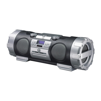
- Page 1 SERVICE MANUAL POWERED WOOFER CD SYSTEM MB519 2006 RV-NB10BJ,RV-NB10BC,RV-NB10BB, RV-NB10BE,RV-NB10BEN,RV-NB10BEV, RV-NB10WJ,RV-NB10WC,RV-NB10WB, RV-NB10WE,RV-NB10WEN Lead free solder used in the board (material : Sn-Ag-Cu, melting point : 219 Centigrade) TABLE OF CONTENTS PRECAUTION............... . . 1-3 SPECIFIC SERVICE INSTRUCTIONS .
- Page 2 SPECIFICATION Amplifier Output Power United States and Canada 6 W per channel, min. RMS, at 4Ω from 150 Hz to 15kHz with no more than 10% total harmonic distortion. 20 W per channel woofer, min. RMS into 4Ω at 60 Hz with no more than 10% total harmonic distortion.
-
Page 3: Precaution
SECTION 1 PRECAUTION Safety Precautions (1) This design of this product contains special hardware and voltmeter. many circuits and components specially for safety purpos- Move the resistor connection to each exposed metal es. For continued protection, no changes should be made part, particularly any exposed metal part having a return to the original design unless authorized in writing by the path to the chassis, and measure the AC voltage across... - Page 4 1.5 Safety Precautions (U.K only) (1) This design of this product contains special hardware and many circuits and components specially for safety purposes. For con- tinued protection, no changes should be made to the original design unless authorized in writing by the manufacturer. Replace- ment parts must be identical to those used in the original circuits.
- Page 5 Preventing static electricity Electrostatic discharge (ESD), which occurs when static electricity stored in the body, fabric, etc. is discharged, can destroy the laser diode in the traverse unit (optical pickup). Take care to prevent this when performing repairs. 1.6.1 Grounding to prevent damage by static electricity Static electricity in the work area can destroy the optical pickup (laser diode) in devices such as laser products.
- Page 6 Important for laser products 5.CAUTION : If safety switches malfunction, the laser is able 1.CLASS 1 LASER PRODUCT to function. 2.DANGER : Invisible laser radiation when open and inter 6.CAUTION : Use of controls, adjustments or performance of lock failed or defeated. Avoid direct exposure to beam. procedures other than those specified here in may result in 3.CAUTION : There are no serviceable parts inside the hazardous radiation exposure.
-
Page 7: Specific Service Instructions
SECTION 2 SPECIFIC SERVICE INSTRUCTIONS This service manual does not describe SPECIFIC SERVICE INSTRUCTIONS. (No.MB519)1-7... -
Page 8: Disassembly
SECTION 3 DISASSEMBLY Main body 3.1.1 Removing the rear cabinet (See Fig.1 to 3) (1) Remove the six screws A (both side) attaching the side protector by 6 angle wrench. (See Fig.1) (2) Remove the eight screws B (both side) attaching the woof- er, and then disconnect the speaker wires. - Page 9 3.1.2 Removing the cassette mechanism assembly (See Fig.4 and 5) (1) Remove the four screws D attaching the cassette mecha- nism. (See Fig.4) CN34 (2) Disconnect the card wires connected to CN33 from display control board. (See Fig.5) Fig.4 CN33 CN34 Fig.5 (No.MB519)1-9...
- Page 10 3.1.3 Removing the CD mechanism assembly (See Fig.3 and 6) (1) Remove the two screws E attaching the CD mechanism CN408 CN407 Tuner boaard assembly. (See Fig.3) (2) Disconnect the card wire connected to CN403 from tuner board. (See Fig.6) (3) Disconnect the card wires connected to CN407 CN408...
- Page 11 3.1.5 Removing the power supply board (See Fig.8 and 9) (1) Disconnect the connector wires connected to CN194 CN191 CN195 from power transformer. (See Fig.8) CN193 (2) Disconnect the connector wires connected to CN191 CN194 CN193 from power amplifier board. (See Fig.8) CN195 (3) Remove the two screws G attaching the power supply board.
- Page 12 3.1.6 Removing the power transformer (See Fig.10) (1) Remove the four screws H attaching the power transform- 3.1.7 Removing the power amplifier board (See Fig.3, 10 and 11) (1) Remove the two screws J attaching the cover. (See Fig.10) (2) Remove the four screws K attaching the heat sink cover. (See Fig.3) (3) Remove the four screws L attaching the power amplifier board.
- Page 13 3.1.8 Removing the display control board (See Fig.12 to 14) (1) Disconnect the connector wire connected to CN751 from CN751 guitar and mic. jack board. (See Fig.12) (2) Remove the four screws M attaching the display control board. (See Fig.13) (3) Disconnect the card wire connected to CN404 from CD...
- Page 14 3.1.9 Removing the CD servo board (See Fig.15 and 16) (1) Remove the four screws N attaching the CD servo board. (See Fig.15) (2) Disconnect the connector wire connected to CN603 from door switch board. (See Fig.15) (3) Disconnect the connector wire connected to feed motor board.
- Page 15 3.1.10 Removing the traverse mechanism (See Fig.17) (1) Remove the four screws P attaching the traverse mecha- nism. Fig.17 3.1.11 Removing the guitar and mic. Jack board (See Fig.18 and 19) (1) Remove the two screws Q attaching the guitar and mic. Jack board.
- Page 16 3.1.12 Removing the front cabinet (See Fig.20 and 21) (1) Remove the eights screws S (both side) attaching the speaker cover. (See Fig.20) (2) Remove the eight screws T (both side) attaching the speaker. (See Fig.21) right side left side Fig.20 Fig.21 1-16 (No.MB519)
- Page 17 3.1.13 Removing the key board (See Fig.22 and 23) (1) Take off the volume and super woofer volume knob. (2) Remove the two nuts U attaching the main volume and su- per woofer volume. (See Fig.22) (3) Remove the eight screws V attaching the key board. (See Fig.23) Fig.22 Fig.23...
- Page 18 3.1.14 Removing the transmitter board (See Fig.24 and 24) (1) Remove the two screws W attaching the transmitter board. (See Fig.24) (2) Pull up the transmitter board with cable. (See Fig.24) Bottom case Fig.24 Fig.25 1-18 (No.MB519)
- Page 19 CD traverse mechanism section • Remove the CD traverse mechanism assembly. (See "3.1.12 Removing the CD traverse mechanism assembly".) 3.2.1 Removing the CD pick (See Figs.1 and 2) (1) Remove the CD mechanism holders in the direction of the CD mechanism holder arrow.
- Page 20 3.2.3 Removing the spindle motor and feed motor (See Fig.2 to 4) (1) Remove the two screws B attaching the feed motor. (See CD mechanism base assembly Fig.2.) (2) Remove the turn table in an upward direction and remove the two screws C attaching the spindle motor. (See Fig.3.) Spindle motor Feed motor (3) From the bottom side of the CD mechanism base assem-...
-
Page 21: See Fig.1 To
Cassette mechanism section • Remove the cassette mechanism assembly. (See "3.1.3 Removing the cassette mechanism assembly".) 3.3.1 Removing the head amplifier & mechanism control board (See Fig.1) (1) After turning over the cassette mechanism assembly, re- move the three screws A attaching the head amplifier & D.C. - Page 22 3.3.3 Removing the flywheels (See Figs.5 and 6) • Remove the head amplifier & mechanism control board and D.C. motor. Flywheel (L) Flywheel (R) (1) After turning over the cassette mechanism assembly, re- move the slit washers (b, c) fixing the capstan shafts R and (2) Pull out the flywheel(R) and flywheel(L) respectively from the bottom side of the cassette mechanism assembly.
- Page 23 3.3.5 Removing the playback/recording head (See Figs.8, 9, 12) (1) While shifting the trigger arms seen on the right side of the head mount assembly in the direction of the arrow, turn the Cassette mechanism assembly flywheel (L) in counterclockwise direction until the head mount assembly has gone out with a click.
- Page 24 3.3.6 Reassembling the playback/recording head (See Figs.10 to 12) (1) Reassemble the head mount. a) To become direction of the left side, direction lever of the head mount assembly is maintained by the hand. (See Fig.11.) b) Reassemble the playback/recording head from the front of the head mount assembly to the position as shown Fig.10, Fig11, and Fig.12.
- Page 25 3.3.7 Reassembling the Control Cam (See Figs.13 to 15) The head assembly is adjusted in the direction of the left side (di- rection of the forward), and it inserts according to the part of the s (hole) Control cam hole s of the control cam and the section s' of the chassis base assembly.
-
Page 26: No.mb519)1
SECTION 4 ADJUSTMENT Connection of adjustment 4.1.1 Connection of cassette deck and circuit board check Key board Display control board Super woofer volume Main volume Volume encoder board Woofer volume encoder board *Remove the key, volume encoder and woofer volume encoder boards from the front cabinet assembly and connect them to the display control board. - Page 27 Adjustment of cassette mechanism section 4.2.1 Arrangement of adjusting points VR32 VR31 VR37 Azimuth adjust screws Adjustment of tape speed Head amplifier & mechanism control board 4.2.2 Electrical performance Measurement Standard Adjusting Items Measurement method conditions values positions AC-225 Adjustment of *Mode : 1.
- Page 28 4.2.3 Reference values for electrical function confirmation items Measurement Standard Adjusting Items Measurement method conditions values positions Recording 100kHz *Recording and 1. While changing over to and from BIAS 1 and 2, bias frequency 6kHz playback side forward confirm that the frequency is changed. or reverse 2.
-
Page 29: Trouble Shooting
SECTION 5 TROUBLE SHOOTING Maintenance of laser pickup (CD) Replacement of laser pickup (CD) (1) Cleaning the pick up lens Before you replace the pick up, please try to clean the lens Turn off the power switch and, disconnect the with a alcohol soaked cotton swab. - Page 30 Victor Company of Japan, Limited Audio/Video Systems Category 10-1,1chome,Ohwatari-machi,Maebashi-city,371-8543,Japan (No.MB519) Printed in Japan...
- Page 31 SCHEMATIC DIAGRAMS POWERED WOOFER CD SYSTEM RV-NB10BJ,RV-NB10BC,RV-NB10BB RV-NB10BE,RV-NB10BEN,RV-NB10BEV RV-NB10WJ,RV-NB10WC,RV-NB10WB RV-NB10WE,RV-NB10WEN CD-ROM No.SML200603 Lead free solder used in the board (material : Sn-Ag-Cu, melting point : 219 Centigrade) Contents Block diagrams Standard schematic diagrams Printed circuit boards 2-29 to 38 No.MB519SCH COPYRIGHT 2006 Victor Company of Japan, Limited.
- Page 32 In regard with component parts appearing on the silk-screen printed side (parts side) of the PWB diagrams, the parts that are printed over with black such as the resistor ( ), diode ( ) and ICP ( ) or identified by the " " mark nearby are critical for safety.
- Page 33 < M E M O >...
-
Page 34: Block Diagram
Block diagram Tuner section FOR Area suffix E/B/EN/EV System control / Function amplifier section LCH,RCH,MPX TDATA FM ANT FM RF/IF/DET/MPX TUCK DATA,CLOCK Q2 to Q6,Q14 AM RF/IF/DET PERIOD AM ANT PERIODE MW/LW SW Tuner section FOR Area suffix J/C LCH,RCH,MPX FM RF/IF/DET/MPX FM ANT DATA,CLOCK,PERIOD... - Page 35 r section Q4101,Q4201 Q4301 AUX MUTE Microphone / Guitar amplifier section FAUX IC752 IC751 VR731 DETECTOR MIC/GUITAR MIC/GUITAR BUFF. AMP Q7360 MIC/ JACK JACK GUITAR JACK Q7358,Q7359 Q7355,Q7356 Q7351 to Q7353 MIC MUTING MIC/GUITAR MIC/GUITAR DRIVE EQ SW GAIN CONT. Q6150 Q5101 IC603...
- Page 36 Standard schematic diagrams I C 6 0 1 T A 8 2 2 3 K Primary section (for J,C) R 6 1 0 1 C 6 1 0 1 0 . 2 2 C 6 2 0 1 2 7 K R 6 2 0 1 2 7 K 0 .
- Page 37 WOOFER AMP L / R P O W E R A M P I C 3 0 1 T A 8 2 3 3 B H 6 0 1 T A 8 2 2 3 K R 6 3 1 5 2 2 0 K C 6 3 0 8 0 .
- Page 38 Primary section (for B,E,EN,EV) I C 6 0 1 T A 8 2 2 3 K R 6 1 0 1 C 6 1 0 1 0 . 2 2 C 6 2 0 1 2 7 K 1 / 4 W C 6 2 0 8 C 6 1 0 8 R 6 2 0 1...
- Page 39 WOOFER AMP L / R P O W E R A M P I C 3 0 1 T A 8 2 3 3 B H 6 0 1 T A 8 2 2 3 K R 6 3 1 5 C 6 3 0 8 2 2 0 K 0 .
- Page 40 Micon / Key control / FL section (for J,C) R E M O C O N T E S T P O I N T C N 9 0 4 Q G A 2 5 0 1 C 3 - 0 3 Z I C 9 0 4 B R 2 4 L 0 2 F - W - X C 9 1 7 8...
- Page 41 L C D L C D D I S P L A Y D I 9 0 1 Q L D 0 3 3 2 - 0 0 2 R 9 2 7 5 4 7 K B 4 1 5 9 R 9 2 7 4 D 9 0 1 4 4 7 K...
- Page 42 Micon / Key control / FL section (for B,E,EN,EV) R E M O C O N T E S T P O I N T C N 9 0 4 Q G A 2 5 0 1 C 3 - 0 3 Z I C 9 0 4 B R 2 4 L 0 2 F - W - X C 9 1 7 8...
- Page 43 L C D L C D D I S P L A Y D I 9 0 1 Q L D 0 3 3 2 - 0 0 2 R 9 2 7 5 4 7 K B 4 1 5 9 R 9 2 7 4 D 9 0 1 4 4 7 K...
- Page 44 Function control section (for J,C) H I G H C O N T . A M P F U N C T I O N A M P C 8 3 5 4 3 3 P C 4 1 4 2 I C 4 0 1 R 8 3 6 1 1 5 P...
- Page 45 R 6 2 6 1 C 6 2 5 0 R 6 2 5 7 1 0 K 4 . 7 K 1 / 5 0 R 6 2 5 0 2 2 K C 6 2 5 1 C 6 2 5 2 I C 6 0 3 1 5 0 P 1 5 0 P...
- Page 46 Function control section (for B,E,EN,EV) H I G H C O N T . A M P F U N C T I O N A M P C 8 3 5 4 3 3 P C 4 1 4 2 I C 4 0 1 N J M 4 5 6 5 M - W E R 8 3 6 1...
- Page 47 C 6 2 5 0 R 6 2 6 1 R 6 2 5 7 1 0 K 4 . 7 K 1 / 5 0 R 6 2 5 0 2 2 K C 6 2 5 1 C 6 2 5 2 I C 6 0 3 1 5 0 P 1 0 0 P...
- Page 48 CD servo control section (for J,C) R601 5.6k TBAL C603 0.1/16 FBAL R602 3.9k TP622 C604 0.1/16 R604 120k C607 TP623 C601 C602 R625 C609 R626 C626 GCTL TP601 C625 R623 R621 C633 0.022 CN601 QGF1008F1-16 R635 R607 /RFDET R606 R608 D601 C617...
- Page 49 CN653 R299 C201 TP17 TP19 TP16 TP18 TP15 R260 TXTCK DRMUTE R261 R267 TXTD EQX5 TP14 TXD0 K253 EQX2 /RST_DSP RXD0 R271 EQX4 REST R266 FLAG IC251 DQSY BLKCK MN101C61GNJ K251 NQR0007-002X D251 K252 CDDOOR R289 NQR0007-002X OUTL R274 RB521S-30-X K250 R258 OUTR...
- Page 50 CD servo control section (for B,E,EN,EV) R601 5.6k TBAL C603 0.1/16 FBAL R602 3.9k TP622 C604 0.1/16 R604 120k C607 TP623 C601 C602 R625 C609 R626 C626 GCTL TP601 C625 R623 R621 C633 0.022 CN601 QGF1008F1-16 R635 R607 /RFDET R606 R608 D601 C617...
- Page 51 CN653 C201 R299 TP17 TP19 TP16 TP18 TP15 R260 TXTCK DRMUTE R261 R267 TXTD EQX5 TP14 TXD0 K253 EQX2 /RST_DSP RXD0 R271 EQX4 REST R266 FLAG IC251 DQSY BLKCK MN101C61GNJ K251 NQR0007-002X D251 K252 CDDOOR R289 NQR0007-002X OUTL R274 RB521S-30-X K250 R258 OUTR...
- Page 52 Cassette mechanism section (common) B406 QUY360-125F Q102 DTC114TKA-X 0.033 C104 R108 5.6K R104 1.2K R102 Q101 1.8K IC31 BA3126N DTC114TKA-X R304 C111 R112 2.2K 0.0012 R111 R301 IC32 AN7317 R211 C211 R212 VGH0425-544 2.2K 0.0012 R207 R202 1.8K R107 R204 1.2K C204 R208...
- Page 53 SG-10SF3 Q102 DTC114TKA-X 1SR139-100T MSI-5U2LWA C111 R112 2.2K FW31 CN32 .0012 QGB2011M1-10 QUM024-06A2Z3 R111 C374 R211 100/10 C211 R212 2.2K 0012 R371 VR37 QVP0008-103Z C307 0.01 Q301 DTA144EKA-X Q371 2SA952/LK/-T Q202 Q375 DTC114TKA-X 2SB562/C/-T D375 R372 R305 HZM5.1NB2-X R338 2.2K 3.9K Q376 2SC2412K/RS/-X...
- Page 54 Mixing mic section (for J,C) Q 7 3 5 7 C 7 3 5 7 2 S C 3 9 2 8 A / R S 9 . 0 V C 7 3 5 6 R 7 3 6 8 P R 7 3 6 2 1 0 0 4 7 / 2 5...
- Page 55 Q 7 3 5 7 2 S C 3 9 2 8 A / R S / - X R 7 3 7 3 1 0 0 K / R S / - X C 7 3 6 1 2 2 0 P R 7 3 7 2 R 7 3 7 1 1 0 K...
- Page 56 Mixing mic section (for B,E,EN,EV) Q 7 3 5 7 C 7 3 5 7 2 S C 3 9 2 8 A / R S 9 . 0 V C 7 3 5 6 R 7 3 6 8 P R 7 3 6 2 1 0 0 4 7 / 2 5...
- Page 57 Q 7 3 5 7 2 S C 3 9 2 8 A / R S / - X R 7 3 7 3 1 0 0 K / R S / - X C 7 3 6 1 2 2 0 P R 7 3 7 1 R 7 3 7 2 1 0 K...
- Page 58 Tuner section (for J,C) P I N N O F M N O S I G N A L 0 . 8 3 . 1 3 . 1 2 . 6 3 . 1 2 . 4 1 . 2 1 .
- Page 59 N O T E S 1 . V O L T A G E S O F T H E T A B L E A R E D C - M E A S U R E D W I T H A D I G I T A L V O L T M E T E R . 2 .
- Page 60 Tuner section (for B,E,EN,EV) 2.2K 2.2K 0.001 3.3K 0.0022 2.2/50 2.2K LC72136N 0.001 2-27...
- Page 61 QFP31HJ-431Z QQR0723-001 0.047 4.7K 4.7K QQR0774-001 180P 100P 0.1/50 TA2008AN 0.012 0.047 0.01 0.012 QQR0719-001 100K 100/16 150P QAX0403-001 1A3G-T1 DATA CLOCK PERIOD 2-28...
- Page 62 Printed circuit boards Main board (for J,C) Lead free solder used in the board (material : Sn-Ag-Cu, melting point : 219 Centigrade) (Power amplifier board) CN603 Q6308 R6322 IC390 D3901 R6307 R3901 C6106 R3195 C3193 D3191 R3200 R6312 R3203 D3192 R3199 Q3191 R3197...
- Page 63 (BAttery spring board) FW603 (Equalizer amplifier board) C5308 R7301 R5107 CN604 R8302 C8303 R8108 R8208 D7301 D7302 R7325 R7323 R8327 R7305 R7326 R7324 R8111 C7302 Q7303 Q8101 R8207 D7303 C8301 R7308 R7331 C8203 D7304 IC701 R7330 D8301 IC704 R7343 R8204 C7301 C7303 R8104...
- Page 64 Main board (except J,C) Lead free solder used in the board (material : Sn-Ag-Cu, melting point : 219 Centigrade) (Power amplifier board) CN603 Q6308 R6322 IC390 D3901 R6307 R3901 C6106 C3193 R3195 D3191 R3200 R6312 R3203 D3192 R3199 Q3191 R3197 R6310 R3191 C6107...
- Page 65 (BAttery spring board) FW603 (Equalizer amplifier board) C5308 R7301 R5107 CN604 R8302 C8303 R8108 R8208 D7301 D7302 R7325 R7323 R7305 R7326 R7324 R8111 C7302 R8327 Q7303 Q8101 R8207 D7303 C8301 R7308 R7331 C8203 D7304 IC701 R7330 D8301 IC704 R7343 R8204 C7301 C7303 R8104...
- Page 66 Micon board (for J,C) Lead free solder used in the board (material : Sn-Ag-Cu, melting point : 219 Centigrade) (Display control board) J901 FW901 R5308 L6352 R6353 R6251 J4301 C6257 R6252 FW403 C6255 C5106 Q8351 R6250 C6251 C5105 C5102 D4302 D8354 R6350 IC603...
- Page 67 (Guitar and Mic. jack board) (Key board) R7367 FW253 C7359 R2511 Q7355 Q7357 C7355 IC751 R7362 C7357 S2501 C7351 R7358 Q7351 S2504 R7354 R7355 R7356 R7386 R7352 R7351 R7357 R7387 S2512 B4064 R7369 C7356 S2503 B7001 R7370 C7360 K7351 C7368 R7376 C7363 R7382...
- Page 68 Micon board (except J,C) Lead free solder used in the board (material : Sn-Ag-Cu, melting point : 219 Centigrade) (Display control board) J901 FW901 R5308 R6251 L6352 R6353 J4301 R6252 C6257 C6255 FW403 C5106 Q8351 R6250 C6251 R6261 C5105 C5102 D4302 D8354 R6350...
- Page 69 (Guitar and Mic. jack board) (Key board) R7367 FW253 C7359 R2511 Q7355 Q7357 C7355 IC751 R7362 C7357 S2501 C7351 R7358 Q7351 S2504 R7354 R7355 R7356 R7386 R7352 R7351 R7357 R7387 S2512 B4064 R7369 C7356 S2503 B7001 R7370 C7360 K7351 C7368 R7376 C7363 R7382...
- Page 70 CD servo control board (common) Lead free solder used in the board (material : Sn-Ag-Cu, melting point : 219 Centigrade) Forward side R617 C663 C659 Q654 C681 R667 C662 C608 K651 R668 C664 C661 R661 C666 R659 R619 R606 C616 C657 R666 R665...
-
Page 71: Switch Board
Cassette mechanism control board (common) Lead free solder used in the board (material : Sn-Ag-Cu, melting point : 219 Centigrade) (Switch board) (Head amplifier board) R371 C376 R341 Q375 CN32 R352 R351 R375 CN34 B152 D375 Q376 C307 B113 B103 C351 Q371 R372... - Page 72 Victor Company of Japan, Limited Audio/Video Systems Category 10-1,1chome,Ohwatari-machi,Maebashi-city,371-8543,Japan Printed in Japan (No.MB519SCH)
-
Page 73: Parts List
PARTS LIST RV-NB10BJ,RV-NB10BC, RV-NB10BB,RV-NB10BE,RV-NB10BEN,RV-NB10BEV, RV-NB10WJ,RV-NB10WC, RV-NB10WB,RV-NB10WE,RV-NB10WEN * All printed circuit boards and its assemblies are not available as service parts. - Contents - 3- 2 Exploded view of general assembly and parts list (Block No.M1) 3- 7 C D mechanism assembly and parts list (Block No.MB) 3- 9 Cassette mechanism assembly and parts list (Block No.MP) - Page 74 Exploded view of general assembly and parts list Block No. Guitar and Mic. jack board CD servo board Tuner board Equalizer amplifie board Key board Display/Control board LED board 40 39 Power supply board 53 148 36 35...
- Page 75 Power amplifier board Tuner board Equalizer amplifier board 40 39 Power supply board...
- Page 76 M3 x 10mm(x6) VJK4516-002 LENS VJD5512-001 LED LENS VYTH539-002 PACKING SHEET L VYTH540-002 PACKING SHEET R QYSBSFG3010ZA TAP SCREW M3 x 10mm PQ45130-7 JVC MARK VJT2389-041 CASSETTE HOLDER NB10BJ,NB10BC,NB10BB,NB10BE,NB10BEN,NB10BEV VJT2389-061 CASSETTE HOLDER NB10WJ,NB10WC,NB10WB,NB10WE,NB10WEN VJT2390-061 DOOR COVER NB10BJ,NB10BC,NB10BB,NB10BE,NB10BEN,NB10BEV VJT2390-071 DOOR COVER NB10WJ,NB10WC,NB10WB,NB10WE,NB10WEN...
- Page 77 Symbol No. Part No. Part Name Description Local LV35864-001A SHIELD B NB10BB,NB10BE,NB10BEN,NB10BEV,NB10WB,NB10WE,NB10WEN LV40779-001A BRACKET QYSBSF3010ZA TAP SCREW M3 x 10mm(x3) LV40759-001A KNOB LV40760-001A MIC PLATE VJT1060-071 CD DOOR NB10BJ,NB10BC,NB10BB,NB10BE,NB10BEN,NB10BEV VJT1060-081 CD DOOR NB10WJ,NB10WC,NB10WB,NB10WE,NB10WEN LV35263-001A CLAMPER LV42929-001A P.C.MAGNET VYH7314-001 YOKE LV43667-001A CLAMPER WEIGHT VXL4458-061...
- Page 78 Symbol No. Part No. Part Name Description Local VYSH101-027 SPACER QYSBSF3010ZA TAP SCREW M3 x 10mm QYSBSF3010ZA TAP SCREW M3 x 10mm VJC2603-041 BATTERY COVER NB10BJ,NB10BC,NB10BB,NB10BE,NB10BEN,NB10BEV VJC2603-071 BATTERY COVER NB10WJ,NB10WC,NB10WB,NB10WE,NB10WEN VYH5657-001 BATTERY SPRING E65923-009 TAPPING SCREW VJD1233-00JUL SIDE PROTECT.AS (x2) NB10BJ,NB10BC VJD1233-00M...
- Page 79 CD mechanism assembly and parts list Block No. FXL-M73-2M Grease & Bond = JVG-31N The parts without symbol number are not service.
- Page 80 CD mechanism Block No. [M][B][M][M] Symbol No. Part No. Part Name Description Local LV10723-002A CD MECHA BASE A OPTIMA-73B2 CD PICK E406777-002SM C.D SHAFT LV31002-001A CD RACK E307745-441SM C.D GEAR 3 QYSDSP2003N SCREW M2 x 3mm(x4) E406750-442SM PINION LV43119-002A T.T PACKING QAR0253-001 FEED MOTOR...
- Page 81 Cassette mechanism assembly and parts list Block No. SLC-S41M Grease =EM-30L =UD-24 =LEN-320M =Mobil-1 The lower side Cassette switch board Head amplifier & Mechanism control board The parts without symbol number are not service.
- Page 82 Cassette mechanism Block No. [M][P][M][M] Symbol No. Part No. Part Name Description Local VKS1165-00N CHASSIS B. ASSY VKS2274-002 REEL GEAR (x2) VKW5286-002 B.T. SPRING (x2) VKS5559-001 PLAY IDLE GEAR VKS5595-002 BLIND LV42013-001A EARTH SPRING SLC-RP1SVM HEAD MOUNT ASSY VKY3149-002 CASSETTE SP.
-
Page 83: Electrical Parts List
Electrical parts list Symbol No. Part No. Part Name Description Local Main board (J,C ver.) D8301 MTZJ4.3B-T2 Z DIODE Block No. [0][1] C1901 QFLC1HJ-683Z M CAPACITOR 0.068uF 50V J Symbol No. Part No. Part Name Description Local ... - Page 84 Symbol No. Part No. Part Name Description Local Symbol No. Part No. Part Name Description Local C8101 QFLC1HJ-563Z M CAPACITOR 0.056uF 50V J R6304 QRE141J-104Y C RESISTOR 100kΩ 1/4W J C8102 QFLC1HJ-563Z M CAPACITOR 0.056uF 50V J R6305 QRE141J-622Y C RESISTOR 6.2kΩ...
- Page 85 Symbol No. Part No. Part Name Description Local Symbol No. Part No. Part Name Description Local L3191 QQL28AK-101 CHOKE COIL 100uH K Q4102 2SD596/4/-X TRANSISTOR Q4102 or 2SD2114K/VW/-X TRANSISTOR QQR0768-001Z BP FILTER Q4201 2SD596/4/-X TRANSISTOR VYH5483-001 SPRING Q4201 or 2SD2114K/VW/-X TRANSISTOR VYH7199-001 BATT.SPRING...
- Page 86 Symbol No. Part No. Part Name Description Local Symbol No. Part No. Part Name Description Local D7351 1SS133-T2 SI DIODE IM C6352 QEKC1CM-226Z E CAPACITOR 22uF 16V M D7352 1SS133-T2 SI DIODE IM C7351 QETN1HM-104Z E CAPACITOR 0.1uF 50V M D7353 1SS133-T2 SI DIODE IM...
- Page 87 Symbol No. Part No. Part Name Description Local Symbol No. Part No. Part Name Description Local R2508 NRSA63J-221X MG RESISTOR 220Ω 1/16W J R5308 NRSA63J-154X MG RESISTOR 150kΩ 1/16W J R2509 NRSA63J-271X MG RESISTOR 270Ω 1/16W J R5501 NRSA63J-153X MG RESISTOR 15kΩ...
- Page 88 Symbol No. Part No. Part Name Description Local Symbol No. Part No. Part Name Description Local R8364 NRSA63J-473X MG RESISTOR 47kΩ 1/16W J R9203 NRSA63J-333X MG RESISTOR 33kΩ 1/16W J R8365 NRSA63J-101X MG RESISTOR 100Ω 1/16W J R9204 NRSA63J-912X MG RESISTOR 9.1kΩ...
- Page 89 Symbol No. Part No. Part Name Description Local Symbol No. Part No. Part Name Description Local X9002 QAX0416-001Z CERA LOCK NRSA63J-101X MG RESISTOR 100Ω 1/16W J NRSA63J-104X MG RESISTOR 100kΩ 1/16W J NRSA63J-472X MG RESISTOR 4.7kΩ 1/16W J QRE141J-104Y C RESISTOR 100kΩ...
- Page 90 Symbol No. Part No. Part Name Description Local Symbol No. Part No. Part Name Description Local C231 NDC31HJ-390X C CAPACITOR 39pF 50V J R266 NRSA63J-102X MG RESISTOR 1kΩ 1/16W J C232 NDC31HJ-390X C CAPACITOR 39pF 50V J R267 NRSA63J-102X MG RESISTOR 1kΩ...
- Page 91 Symbol No. Part No. Part Name Description Local Symbol No. Part No. Part Name Description Local R837 NRSA63J-271X MG RESISTOR 270Ω 1/16W J Q6306 KRC102M-T DIGI TRANSISTOR R838 NRSA63J-271X MG RESISTOR 270Ω 1/16W J Q6307 KRC102M-T DIGI TRANSISTOR R839 NRSA63J-271X MG RESISTOR...
- Page 92 Symbol No. Part No. Part Name Description Local Symbol No. Part No. Part Name Description Local QCBB1HK-151Y C CAPACITOR 150pF 50V K C8102 QFLC1HJ-563Z M CAPACITOR 0.056uF 50V J QCBB1HK-222Y C CAPACITOR 2200pF 50V K C8103 QETN1EM-476Z E CAPACITOR 47uF 25V M QETN1HM-225Z E CAPACITOR...
- Page 93 Symbol No. Part No. Part Name Description Local Symbol No. Part No. Part Name Description Local R3310 QRE141J-681Y C RESISTOR 680Ω 1/4W J R7322 QRE141J-563Y C RESISTOR 56kΩ 1/4W J R3311 QRE141J-681Y C RESISTOR 680Ω 1/4W J R7323 NRSA63J-102X MG RESISTOR 1kΩ...
- Page 94 Symbol No. Part No. Part Name Description Local Symbol No. Part No. Part Name Description Local IC551 PQ033ES3MX-T Q8351 or 2SB709A/QR/-X TRANSISTOR IC603 NJM4565M-WE Q8352 2SA1530A/QR/-X TRANSISTOR IC751 NJM4565M-WE Q8352 or 2SB709A/QR/-X TRANSISTOR IC752 NJM4565M-WE Q8353 2SC3928A/RS/-X TRANSISTOR IC831 NJM4565M-WE Q8353 or 2SD601A/R/-X...
- Page 95 Symbol No. Part No. Part Name Description Local Symbol No. Part No. Part Name Description Local C4343 NCS31HJ-151X C CAPACITOR 150pF 50V J C8363 NCS31HJ-101X C CAPACITOR 100pF 50V J C4344 QEKC1HM-226Z E CAPACITOR 22uF 50V M C9001 QER61AM-107Z E CAPACITOR 100uF 10V M...
- Page 96 Symbol No. Part No. Part Name Description Local Symbol No. Part No. Part Name Description Local R4142 NRSA63J-303X MG RESISTOR 30kΩ 1/16W J R7353 NRSA63J-393X MG RESISTOR 39kΩ 1/16W J R4143 NRSA63J-224X MG RESISTOR 220kΩ 1/16W J R7354 NRSA63J-153X MG RESISTOR 15kΩ...
- Page 97 Symbol No. Part No. Part Name Description Local Symbol No. Part No. Part Name Description Local R9120 NRSA63J-103X MG RESISTOR 10kΩ 1/16W J L4354 NQR0007-002X FERRITE BEADS R9124 NRSA63J-222X MG RESISTOR 2.2kΩ 1/16W J L4355 NQR0007-002X FERRITE BEADS R9125 NRSA63J-103X MG RESISTOR...
- Page 98 Symbol No. Part No. Part Name Description Local Symbol No. Part No. Part Name Description Local J1901 QNC0003-001 AC SOCKET C665 NCB31CK-104X C CAPACITOR 0.1uF 16V K J1902 QNA0016-001 DC JACK C666 QEKJ0JM-107Z E CAPACITOR 100uF 6.3V M ...
- Page 99 Symbol No. Part No. Part Name Description Local Symbol No. Part No. Part Name Description Local R662 NRSA02J-101X MG RESISTOR 100Ω 1/10W J Q201 DTC114TKA-X TRANSISTOR R664 NRSA63J-102X MG RESISTOR 1kΩ 1/16W J Q202 DTC114TKA-X TRANSISTOR R665 NRSA63J-681X MG RESISTOR 680Ω...
- Page 100 Symbol No. Part No. Part Name Description Local Symbol No. Part No. Part Name Description Local R101 NRSA63J-220X MG RESISTOR 22Ω 1/16W J QSW0832-001 CASS.SWITCH R102 NRSA63J-182X MG RESISTOR 1.8kΩ 1/16W J QSW0832-001 CASS.SWITCH R103 NRSA63J-242X MG RESISTOR 2.4kΩ...
- Page 101 < MEMO > 3-29...
- Page 102 Packing materials and accessories parts list Block No. No additional / supplemental order of WARRANTY CARDs are available A1,A2,A6,A8, A11, A12, 3-30...
- Page 103 Packing and Accessories Block No. [M][3][M][M] Symbol No. Part No. Part Name Description Local LVT1539-001A INST BOOK NB10BJ,NB10WJ LVT1539-002A INST BOOK ENG FRE NB10BC,NB10WC LVT1539-003A INST BOOK NB10BB,NB10WB LVT1539-004A INST BOOK GER FRE NB10BE,NB10WE LVT1539-006A INST BOOK SWE FIN DAN NB10BEN,NB10WEN LVT1539-008A INST BOOK...
Need help?
Do you have a question about the RV-NB10BJ and is the answer not in the manual?
Questions and answers