Phytec phyCORE-AM335x Hardware Manual
Hide thumbs
Also See for phyCORE-AM335x:
- Quick start instructions (92 pages) ,
- Quick start manual (2 pages)
Table of Contents
Advertisement
Quick Links
Advertisement
Table of Contents

Related Manuals for Phytec phyCORE-AM335x


Summary of Contents for Phytec phyCORE-AM335x
- Page 1 Hardware Manual Document No: L-771e_1 SOM Product No:PCM-051 SOM PCB No:1358.2 Carrier Board Product No:PCM-953 Carrier Board PCB No:1359.2 GPIO Expansion Board Product No: PCM-957 Edition November 2012 A product of a PHYTEC Technology Holding company...
- Page 2 PHYTEC Messtechnik GmbH reserves the right to alter the information contained herein without prior notification and accepts no responsibility for any damages which might result.
-
Page 3: Table Of Contents
Table of content Table of Contents Conventions, Abbreviations and Acronyms ..........1 Preface....................4 Part I: PCM-051/phyCORE-AM335x System on Module ....... 8 3.1 Introduction ................. 8 3.1.1Block Diagram ...............10 3.1.2Component Placement Diagram ..........11 3.1.3Minimum Requirements to Operate the phyCORE-AM335x....13 3.2 Pin Description ................14... - Page 4 3.13.1Parallel Display Interface............55 3.13.2Touch Screen Controller ............56 3.14 Technical Specifications ..............57 3.15 Hints for Integrating and Handling the phyCORE-AM335x ..... 59 3.15.1Integrating the phyCORE-AM335x ........... 59 3.15.2Handling the phyCORE-AM335x ..........61 Part II: PCM-953 / phyCORE-AM335x Carrier Board ........62 4.1 Introduction................
- Page 5 5.4 GPIO Expansion Board GPMC Signals ..........109 5.5 GPIO Expansion Board Power Signals ..........109 5.6 GPIO Expansion Board Serial Interfaces ........... 110 5.7 Signals Not Connected to the GPIO Expansion Board ......111 © 2012 L-771e_1 PHYTEC Messtechnik GmbH...
- Page 6 Table 27: Table 28: I2C Interface Signal Locations................48 Table 29: I2C Addresses in Use ..................48 SPI0 Interface Signal Locations ................48 Table 30: Table 31: DCAN0 and DCAN1 Signal Locations..............49 Table 32: McASP Signal Locations ..................50 © 2012 L-771e_1 PHYTEC Messtechnik GmbH...
- Page 7 Table 36: Table 37: Parallel Display Interface Signal Locations............55 Table 38: AIN[3:0] Signal Locations ................56 phyCORE-AM335x Carrier Board Connectors and Pin Headers ........65 Table 39: Table 40: phyCORE-AM335x Carrier Board push-buttons Descriptions........67 Table 41: Carrier Board Boot Configuration Switch S5 ............68 phyCORE-AM335x Carrier Board LEDs Descriptions..........69...
- Page 8 GPIO Expansion Board GPMC Signal Map ............109 Table 68: GPIO Expansion Board Power Signal Map ............109 GPIO Expansion Board Serial Interfaces Signal Map ..........110 Table 69: AM335x SOM Signals Not Routed to the GPIO Expansion Connector X5 ....111 Table 70: © 2012 PHYTEC Messtechnik GmbH L-771e_1...
- Page 9 Physical Dimensions..................57 Figure 9: Figure 10: Footprint of the phyCORE-AM335x ..............60 Figure 11: phyCORE-AM335x Carrier Board Overview of Connectors and Buttons (top view)..64 Figure 12: Carrier Board Buttons..................66 Figure 13: Switch S5 Location ..................67 Figure 14: Carrier Board LEDs ..................69 Figure 15: Jumper Numbering Scheme ................70...
-
Page 10: Conventions, Abbreviations And Acronyms
Section Note: The BSP delivered with the phyCORE-AM335x usually includes drivers and/or software for controlling all components such as interfaces, memory, etc.. Therefore programming close to hardware at register level is not necessary in most cases. For this reason, this manual contains no detailed description of the controller's registers, or information relevant for software development. -
Page 11: Table 1: Abbreviations And Acronyms Used In This Manual
Real-time clock Surface mount technology System on Module; used in reference to the PCM-051 / phyCORE-AM335x System on Module User button Sx (e.g. S1, S2, etc.) used in reference to the available user buttons, or DIP switches on the carrier board Sx_y Switch y of DIP switch Sx;... -
Page 12: Table 2: Types Of Signals
Differential line pairs 100 Ohm LVDS Pegel LVDS Differential 90 Ohm Differential line pairs 90 Ohm DIFF90 Differential 100 Ohm Differential line pairs 100 Ohm DIFF100 Analog Analog input or output Analog Table 2: Types of Signals © 2012 PHYTEC Messtechnik GmbH L-771e_1... -
Page 13: Preface
Preface 2 Preface As a member of PHYTEC's phyCORE product family the phyCORE-AM335x is one of a series of PHYTEC System on Modules (SOMs) that can be populated with different controllers and, hence, offers various functions and configurations. PHYTEC supports a variety of 8-/16- and 32-bit controllers in two ways: 1. - Page 14 The structure shows the ordering options available as of the printing of this manual. Additional ordering options may have been added. Please contact our sales team to ´get an update on the ordering options available. © 2012 PHYTEC Messtechnik GmbH L-771e_1...
- Page 15 Caution: PHYTEC products lacking protective enclosures are subject to damage by ESD and, hence, may only be unpacked, handled or operated in environments in which sufficient precautionary measures have been taken in respect to ESD-dangers. It is also necessary that only appropriately trained personnel (such as electricians, technicians and engineers) handle and/or operate these products.
- Page 16 Product Change Management and information in this manual on parts populated on the SOM When buying a PHYTEC SOM, you will, in addition to our HW and SW offerings, receive a free obsolescence maintenance service for the HW we provide.
-
Page 17: Part I: Pcm-051/Phycore-Am335X System On Module
Part I: PCM-051/phyCORE-AM335x System on Module 3 Part I: PCM-051/phyCORE-AM335x System on Module Part I of this three part manual provides detailed information on the phyCORE-AM335x System on Module (SOM) designed for custom integration into customer applications. The information in the following chapters is appli- cable to the 1358.2 PCB revision of the phyCORE-AM335x SOM. - Page 18 Otherwise individual signals may have bad, or no contact. The maximum memory size listed is as of the printing of this manual. Please contact PHYTEC for more information about additional, or new module configurations available.
-
Page 19: 1Block Diagram
Part I: PCM-051/phyCORE-AM335x System on Module 3.1.1 Block Diagram Figure 1: Block Diagram of the phyCORE-AM335x L-771e_1 © PHYTEC Messtechnik GmbH 2012... -
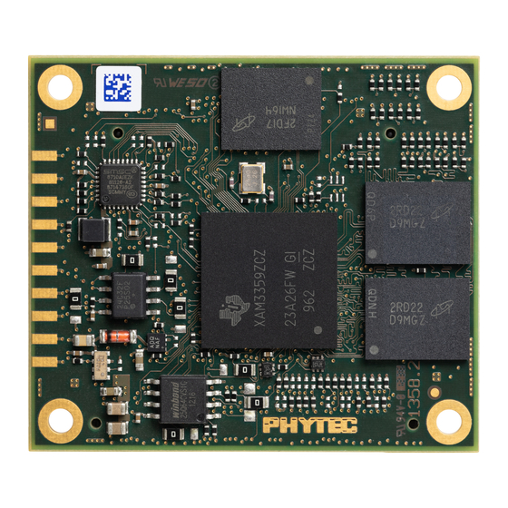
Page 20: 2Component Placement Diagram
Part I: PCM-051/phyCORE-AM335x System on Module phyCORE-AM335x 3.1.2 Component Placement Diagram Figure 2: phyCORE-AM335x Component Placement (top view) © 2012 PHYTEC Messtechnik GmbH L-771e_1... -
Page 21: Figure 3: Phycore-Am335X Component Placement (Bottom View)
Part I: PCM-051/phyCORE-AM335x System on Module Figure 3: phyCORE-AM335x Component Placement (bottom view) L-771e_1 © PHYTEC Messtechnik GmbH 2012... -
Page 22: 3Minimum Requirements To Operate The Phycore-Am335X
3.1.3 Minimum Requirements to Operate the phyCORE-AM335x Basic operation of the phyCORE-AM335x requires only supply of a +5.0 V input voltage with minimum 2.0 A capacity and the corresponding GND connections. These supply pins are located at the phyCORE-Connector X3:... -
Page 23: Pin Description
Carrier Board/user target circuitry. The upper left-hand corner of the numbered matrix (pin 1A) is thus covered with the corner of the phyCORE-AM335x marked with a triangle. The numbering scheme is always in relation to the PCB as viewed from above, even if all connector contacts extend to the bottom of the module. -
Page 24: Figure 4: Pinout Of The Phycore-Connector (Top View, With Cross Section Insert)
Table 3 provides an overview of the pinout of the phyCORE-Connector with signal names and descriptions specific to the phyCORE-AM335x. It also provides the appropriate signal level interface voltages listed in the SL (Signal Level) column and the signal direction. -
Page 25: Table 3: Pinout Of The Phycore-Connector X3, Row A
Part I: PCM-051/phyCORE-AM335x System on Module Pin Row X3A Pin # Signal Type Description Ground 0 V VBAT_IN_4RTC 3 V - 5 V Optional always-on power for the Real-Time Clock (RTC). If a backup batter is not used, connect this pin to the primary 5V supply. - Page 26 Part I: PCM-051/phyCORE-AM335x System on Module phyCORE-AM335x Pin Row X3A Pin # Signal Type Description X_MII1_TXD2 3.3 V Ethernet 1 MII transmit data X_MII1_TXD3 3.3 V Ethernet 1 MII transmit data Ground 0 V X_MCASP0_AHCLKX 3.3 V Multi-channel Audio Serial Port 0 Tx bit clock X_MCASP0_AXR1 3.3 V...
-
Page 27: Table 4: Pinout Of The Phycore-Connector X3, Row B
Part I: PCM-051/phyCORE-AM335x System on Module Pin Row X3A Pin # Signal Type Description X_LCD_D14 / P_MII0_MR_CLK IO 3.3 V LCD data 14 or PRU Ethernet 0 Rx clock X_LCD_D15 / P_MII0_RXDV 3.3 V LCD data 15 or PRU Ethernet Rx data valid X_LCD_D6 3.3 V... - Page 28 Part I: PCM-051/phyCORE-AM335x System on Module phyCORE-AM335x Pin Row X3B Pin # Signal Type Description Ground 0 V X_USB1_DRVVBUS 3.3 V USB 1 VBUS control output X_USB1_VBUS 5.0 V USB 1 bus voltage X_USB1_ID USB 1 port identification. 1.8 V logic.
-
Page 29: Table 5: Pinout Of The Optional Phycore-Connector X1, Row A
Part I: PCM-051/phyCORE-AM335x System on Module Pin Row X3B Pin # Signal Type Description Ground 0 V X_MMC0_CLK 3.3 V MMC / SDIO 0 clock X_MMC0_CMD 3.3 V MMC / SDIO 0 command X_MMC0_D0 3.3 V MMC / SDIO 0 data 0 X_MMC0_D1 3.3 V... - Page 30 Part I: PCM-051/phyCORE-AM335x System on Module phyCORE-AM335x Pin Row X1A (Optional Connector) Pin # Signal Type SL Description X_RMII1_CRS / MCASP1_ACLKX 3.3 V Ethernet1 RMII carrier sense or Multi- channel Audio Serial Port 1 Tx bit clock X_GPMC_AD1 3.3 V...
- Page 31 Part I: PCM-051/phyCORE-AM335x System on Module Pin Row X1A (Optional Connector) Pin # Signal Type SL Description X_RGMII2_TD3 / MMC2_DAT1 / P_MII1_TXD2 IO 3.3 V Ethernet 2 RGMII Tx data 3 or MMC/SDIO 2 data 1 or PRU Ethernet1 Tx data 2...
-
Page 32: Table 6: Pinout Of The Optional Phycore-Connector X1, Row B
Part I: PCM-051/phyCORE-AM335x System on Module phyCORE-AM335x Pin Row X1B (Optional Connector) Pin # Signal Type SL Description X_SPI_WPn 3.3 V SPI FLASH write-protect (low-true) X_MDIO_DATA 3.3 V Ethernet MDIO interface data X_MDIO_CLK 3.3 V Ethernet MDIO interface clock Ground 0 V X_GPIO_3_18 3.3 V... - Page 33 Part I: PCM-051/phyCORE-AM335x System on Module Pin Row X1B (Optional Connector) Pin # Signal Type SL Description Ground 0 V X_LCD_D20 3.3 V LCD data X_LCD_D19 3.3 V LCD data X_LCD_D18 3.3 V LCD data X_P_MII1_TXEN 3.3 V PRU Ethernet 1 MII Tx enable...
-
Page 34: Jumpers
Part I: PCM-051/phyCORE-AM335x System on Module phyCORE-AM335x 3.3 Jumpers For configuration purposes, the phyCORE-AM335x has ten solder jumpers. These have been installed prior to delivery. Figure 5 depicts the jumper pad numbering scheme for reference when altering jumper settings on the board. -
Page 35: Figure 6: Som Jumper Locations (Top View)
Part I: PCM-051/phyCORE-AM335x System on Module Figure 6: SOM Jumper Locations (top view) If manual jumper modification is required please ensure that the board as well as surrounding components and sockets remain undamaged while de-soldering. Overheating the board can cause the solder pads to loosen, rendering the module inoperable. -
Page 36: Table 7: Som Jumper Settings
Part I: PCM-051/phyCORE-AM335x System on Module phyCORE-AM335x The jumpers on the AM335x SOM have the following functions: Jumper Setting Description Type Chapter J1 routes CLKOUT1 to either the phy- 0R (0805) CORE-Connector or to the Ethernet1 transceiver's clock input. CLKOUT1 can be used for the Ethernet refereence clock if the Ethernet1 inter- face is running in MII mode. - Page 37 Part I: PCM-051/phyCORE-AM335x System on Module Jumper Setting Description Type Chapter J4 connects the low-true write-protect 0R (0805) input of the SPI-Flash (U5) to one of three signals: 1. the power-on reset signal, X_PORZ. This prevents data corruption during power-up.
- Page 38 Part I: PCM-051/phyCORE-AM335x System on Module phyCORE-AM335x Jumper Setting Description Type Chapter Selects the COL/CRS signal for the 0R (0402) Ethernet1 transceiver depending on whether it is running in MII or RMII mode. Table 23 Selects the COL/CRS signal for RMII mode Selects the COL/CRS signal for MII mode.
-
Page 39: Power
3.4.2 Backup Power (VBAT_IN_4RTC) To backup the RTC on the module, a secondary voltage source of 3 V can be attached to the phyCORE-AM335x at pin X3.A2. This voltage source supplies the backup voltage domain VBACKUP of the phyCORE-AM335x which supplies the RTC (either the RTC integrated in the PMIC or the external RTC) and some critical registers when the primary system power (VCC_5V_IN) is removed. -
Page 40: Power Domains
The PMIC has two input voltage rails VDD_5V_IN and VBAT_IN_4RTC, as can be seen in Figure 7 VDD_5V_IN is supplied from the primary voltage input pins VDD_5V_IN of the phyCORE-AM335x. VBAT_IN_4RTC may optionally be supplied to the PMIC from the secondary voltage input pin X3.A3 through jumper J10. -
Page 41: Real Time Clock (Rtc)
Part I: PCM-051/phyCORE-AM335x System on Module Figure 7: Power Supply Diagram 3.4.3.2 Real Time Clock (RTC) The PMIC, which is populated on the module, provides a real time clock (RTC) with alarm and timekeeping functions. The RTC is supplied by the backup voltage VBAT_IN_4RTC when the main power supply VDD_5V_IN is not applied if jumper J10 is installed at (2+3). -
Page 42: Power Management
Part I: PCM-051/phyCORE-AM335x System on Module phyCORE-AM335x 3.4.3.3 Power Management The PMIC provides different power management functions. Two signals to control the power-on/off state of the system (X_PB_POWER and X_PMIC_POWER_EN) are available. The following table shows the power management signals and their functions. -
Page 43: Real-Time Clock Options (Rtc)
Part I: PCM-051/phyCORE-AM335x System on Module 3.5 Real-Time Clock Options (RTC) There are three options for an RTC on the AM335x-SOM. 3.5.1 PMIC RTC The default RTC is the one integrated in the Power Management IC at U4. This RTC includes alarm and timekeeping functions. -
Page 44: System Configuration And Booting
The following tables show the different boot device orders, which can be selected by configuring the five boot- order configuration pins, X_LCD_D[4:0] of the phyCORE-AM335x. Please note that only a subset of possible configurations are listed in the tables. For a complete list of the AM335x boot modes please refer to the Texas Instruments AM335x Technical Reference Manual. -
Page 45: Table 11: Boot Device Order Of Am335X Module
Part I: PCM-051/phyCORE-AM335x System on Module Boot Mode Selec- Booting Device Order tion X_LCD_D[4:0] 00010 UART0 SPI0 NAND NANDI2C 00110 EMAC1 SPI0 NAND NANDI2C 01011 USB0 NAND SPI0 MMC0 10010 NAND NANDI2C USB0 UART0 10011 NAND NANDI2C MMC0 UART0... -
Page 46: System Memory
3.7.1 DDR3-SDRAM (U7, U9) The RAM memory of the phyCORE-AM335x is comprised of two 8-bit wide DDR3-SDRAM chips at U7 and U9. The effective bus is 16-bits wide. The chips are connected to the dedicated DDR interface called the Extended Memory Interface (EMIF) of the AM335x processor. -
Page 47: Nand Flash Lock Control (J2)
3.7.3 I C EEPROM (U6) The phyCORE-AM335x can be populated with a non-volatile 4 KB EEPROM with an I C interface as an ordering option. This memory can be used to store configuration data or other general purpose data. This device is accessed through I C port 0 on the AM335x. -
Page 48: Setting The Eeprom Lower Address Bits (J7, J8)
3.7.3.1 Setting the EEPROM Lower Address Bits (J7, J8) The I²C EEPROM populating U6 on the phyCORE-AM335x SOM allows the user to configure the lower address bits A0, A1, and A2. The four upper address bits of the 7-bit address are fixed at ‘1010’. On the SOM, A0 is tied to GND. -
Page 49: 4Spi Flash Memory (U5)
Part I: PCM-051/phyCORE-AM335x System on Module 3.7.4 SPI Flash Memory (U5) The phyCORE-AM335x can be populated with a SPI Flash memory device as an ordering option. This would be suitable for applications which require a small code footprint or small RTOSes. -
Page 50: Sd / Mmc Card Interfaces
Part I: PCM-051/phyCORE-AM335x System on Module phyCORE-AM335x 3.8 SD / MMC Card Interfaces The phyCORE-AM335x includes three SD / MMC Card interfaces: MMC0, MMC1 and MMC2. Table 18 shows the location of the MMC0 interface signals identified on the phyCORE-Connector. -
Page 51: Serial Interfaces
Part I: PCM-051/phyCORE-AM335x System on Module 3.9 Serial Interfaces The phyCORE-AM335x provides numerous serial interfaces, some of which are equipped with a transceiver to allow direct connection to external devices: 1. Up to four high speed Universal Asynchronous Receiver/Transmitter (UART) interfaces with up to 3.6 Mbps at TTL level. -
Page 52: 2Usb Otg Interface
USB-OTG PHY. An external USB Standard-A (for USB host), USB Standard-B (for USB device), or USB mini-AB (for USB OTG) connector is all that is needed to inteface the phyCORE-AM335x USB OTG functionality. The appli- cable interface signals can be found on the phyCORE-Connector as shown in... -
Page 53: 3Ethernet Interfaces
Part I: PCM-051/phyCORE-AM335x System on Module 3.9.3 Ethernet Interfaces Connection of the phyCORE-AM335x to the world wide web or a local area network (LAN) is possible using the AM335x processor's integrated 10/100/1000 Ethernet switch. The switch has two ports: Ethernet1 and Ethernet2. -
Page 54: Configuring The Ethernet1 Interface Mode
3.9.3.1.1 Configuring the Ethernet1 Interface Mode The phyCORE-AM335x design allows the transceiver on the Ethernet1 interface to run in either RMII or MII mode. The RMII mode has the advantage that it uses fewer signals than MII mode, freeing up some signals to be used for other uses, including UART2, UART3 and DCAN0. -
Page 55: Ethernet 2
Part I: PCM-051/phyCORE-AM335x System on Module Resistor RMII Package do not install 0402 10 kOhm 100 Ohm do not install 0402 100 Ohm 0402 do not install 10 kOhm do not install 0402 do not install 0402 0 Ohm... -
Page 56: 4Profibus
Part I: PCM-051/phyCORE-AM335x System on Module phyCORE-AM335x Pin# Signal name Type Description X1B42 X_RGMII2_TCTL 3.3 V RGMII or RMII transmit control, MII transmit enable X1A41 X_RGMII2_TCLK 3.3 V RGMII or MII transmit clock X1A36 X_RGMII2_TD3 3.3 V RGMII or MII transmit data bit 3... -
Page 57: 5I2C Interface
Part I: PCM-051/phyCORE-AM335x System on Module 3.9.5 I C Interface The Inter-Integrated Circuit (I C) interface is a two-wire, bi-directional serial bus that provides a simple and efficient method for data exchange among devices. The AM335x contains three identical and independent I modules. -
Page 58: 7Controller Area Network (Can) Interfaces
Part I: PCM-051/phyCORE-AM335x System on Module phyCORE-AM335x 3.9.7 Controller Area Network (CAN) Interfaces The Controller Area Network (CAN) is a serial communications protocol which efficiently supports distributed real time control with a high level of security. The AM335x includes two CAN interfaces, DCAN0 and DCAN1. These support bitrates up to 1 MBit/s and are compliant to the CAN 2.0B protocol specification. -
Page 59: 8Multichannel Audio Serial Ports (Mcasp)
Part I: PCM-051/phyCORE-AM335x System on Module 3.9.8 Multichannel Audio Serial Ports (McASP) The two multichannel audio serial port (McASP) interfaces of the phyCORE-AM335x are general audio serial ports optimized for the requirements of various audio applications. The McASP is useful for intercomponent digital audio interface transmission (DIT). -
Page 60: General Purpose I/Os
Its maximum load is 150 mA. To support all features of the phyCORE-AM335x Carrier Board special functions have been assigned to the GPIOs in the BSP delivered with the module. In order to otherwise utilize the GPIOs the software must be changed. -
Page 61: Analog Inputs
Note: To support the display touch-control feature of the phyCORE-AM335x Carrier Board, the touch-control function has been assigned to the four analog input signals X_AIN0 to X_AIN3 in the BSP delivered with the module. In order to otherwise utilize these signals, the software must be changed. -
Page 62: Debug Interface (X2)
3.12 Debug Interface (X2) The phyCORE-AM335x is equipped with a JTAG interface for downloading program code into the external flash, internal controller RAM or for debugging programs which are executing. The JTAG interface connects to a 2.54 mm pitch pin header at X2 on the edge of the module PCB and also to the optional phyCORE-Connector X1. -
Page 63: Table 35: Jtag Connector X2 Signal Assignment
Part I: PCM-051/phyCORE-AM335x System on Module The JTAG edge card connector X2 provides an easy means of debugging the phyCORE-AM335x in your target system via an external JTAG probe. Note: The JTAG connector X2 only populates phyCORE-AM335x modules with order code PCM-051-xxxxxxxJxx. -
Page 64: Display Interface
Part I: PCM-051/phyCORE-AM335x System on Module phyCORE-AM335x 3.13 Display Interface The phyCORE-AM335x provides a configurable parallel display interface with up to 24 data bits and backlight and touch-screen control. 3.13.1 Parallel Display Interface The 24-bit integrated LCD Interface Display Driver (LIDD) of the AM335x is directly connected to the phyCORE- Connector. -
Page 65: 2Touch Screen Controller
The AM335x’s eight analog signals, AIN[7:0], are routed to the primary phyCORE connector, X3. Some or all of these can be connected to a resistive touch panel. The PHYTEC carrier board connects four of these signals to a touch screen integrated in a LCD display. These signals are mapped as follows:... -
Page 66: Technical Specifications
Part I: PCM-051/phyCORE-AM335x System on Module phyCORE-AM335x 3.14 Technical Specifications The physical dimensions of the phyCORE-AM335x are represented in Figure 9 . The module's profile is max. 5.0 mm thick, with a maximum component height of 1.5 mm on the bottom (connector) side of the PCB and approximately 2.0 mm on the top (microcontroller) side. -
Page 67: L-771E_1 © Phytec Messtechnik Gmbh
In order to guarantee reliable functioning of the SOM up to the maximum temperature appropriate cooling measures must be provided. Use of the SOM at high temperature impacts the SOM's life span. These specifications describe the standard configuration of the phyCORE-AM335x as of the printing of this manual. -
Page 68: Hints For Integrating And Handling The Phycore-Am335X
Part I: PCM-051/phyCORE-AM335x System on Module phyCORE-AM335x 3.15 Hints for Integrating and Handling the phyCORE-AM335x 3.15.1 Integrating the phyCORE-AM335x Successful integration in user target circuitry greatly depends on the adherence to the layout design rules for the GND connections of the phyCORE module. As a general design rule we recommend connecting all GND pins neighboring signals which are being used in the application circuitry. -
Page 69: Figure 10: Footprint Of The Phycore-Am335X
Part I: PCM-051/phyCORE-AM335x System on Module Figure 10: Footprint of the phyCORE-AM335x L-771e_1 © PHYTEC Messtechnik GmbH 2012... -
Page 70: 2Handling The Phycore-Am335X
Part I: PCM-051/phyCORE-AM335x System on Module phyCORE-AM335x 3.15.2 Handling the phyCORE-AM335x Removal of various components, such as the microcontroller and the standard quartz, is not advisable given the compact nature of the module. Should this nonetheless be necessary, please ensure that the board as well as surrounding components and sockets remain undamaged while de-soldering.
Need help?
Do you have a question about the phyCORE-AM335x and is the answer not in the manual?
Questions and answers