Table of Contents
Advertisement
TABLE OF CONTENTS
1 Safety Precautions----------------------------------------------- 3
1.1. General Guidelines---------------------------------------- 3
1.2. Caution for AC Mains Lead (For EB only)----------- 4
1.3. Before Repair and Adjustment ------------------------- 4
1.4. Protection Circuitry ---------------------------------------- 4
1.5. Caution For Fuse Replacement------------------------ 4
1.6. Safety Part Information----------------------------------- 5
2 Warning -------------------------------------------------------------- 6
to Electrostatically Sensitive (ES) Devices---------- 6
3 Service Navigation ----------------------------------------------- 8
3.1. Service Information --------------------------------------- 8
4 Specifications ----------------------------------------------------- 9
5 Location of Controls and Components ------------------10
6 Self Diagnostic Mode ------------------------------------------11
7 Disassembly and Assembly Instructions ---------------12
7.1. Disassembly flow chart----------------------------------13
7.2. Types of Screws ------------------------------------------13
7.3. Main Parts Location Diagram--------------------------14
7.4. Disassembly of Rear Cabinet Block -----------------15
Downloaded from
www.Manualslib.com
manuals search engine
RF-D10EB
Model No.
RF-D10EG
RF-D10GN
Product Color: (K)...Black Type
(W)...White Type (EG, GN)
PAGE
7.6. Disassembly of D-AMP P.C.B.------------------------ 17
7.7. Disassembly of Volume P.C.B. ----------------------- 18
7.8. Disassembly of Main P.C.B. --------------------------- 19
Headphone P.C.B. --------------------------------------- 22
7.10. Disassembly of Speaker (SP1) ----------------------- 25
8 Service Position ------------------------------------------------- 26
8.1. Checking of Power P.C.B. ----------------------------- 26
8.2. Checking of D-AMP P.C.B. ---------------------------- 27
8.3. Checking of Main P.C.B. (Side A) ------------------- 28
8.4. Checking of Main P.C.B. (Side B) ------------------- 30
9 Wiring Connection Diagram--------------------------------- 33
10 Schematic Diagram -------------------------------------------- 35
10.1. Schematic Diagram Notes ----------------------------- 35
10.2. MAIN CIRCUIT ------------------------------------------- 37
CIRCUIT---------------------------------------------------- 38
BATTERY (+) CIRCUIT--------------------------------- 39
© Panasonic Corporation 2014. All rights reserved.
Unauthorized copying and distribution is a violation of
law.
PSG1401003CE
DAB-FM Radio
PAGE
Advertisement
Table of Contents

Related Manuals for Panasonic RF-D10EG


Summary of Contents for Panasonic RF-D10EG
-
Page 1: Table Of Contents
7.3. Main Parts Location Diagram--------------------------14 10.4. TOP KEY / POWER / BATTERY (-) / 7.4. Disassembly of Rear Cabinet Block -----------------15 BATTERY (+) CIRCUIT--------------------------------- 39 © Panasonic Corporation 2014. All rights reserved. Unauthorized copying and distribution is a violation of law. Downloaded from www.Manualslib.com... - Page 2 11 Printed Circuit Board ------------------------------------------ 40 11.1. MAIN P.C.B. ----------------------------------------------- 40 11.2. DAMP / VOLUME / LED / HEADPHONE P.C.B.-------------------------------------------------------- 41 11.3. TOP KEY / POWER / BATTERY (-) / BATTERY (+) P.C.B.------------------------------------- 42 12 Appendix Information of Schematic Diagram --------- 43 12.1.
-
Page 3: Safety Precautions
1 Safety Precautions 1.1. General Guidelines 1. IMPORTANT SAFETY NOTICE There are special components used in this equipment which are important for safety. These parts are marked by in the Schematic Diagrams, Circuit Board Layout, Exploded Views and Replacement Parts List. It is essential that these critical parts should be replaced with manufacturer’s specified parts to prevent X-RADIATION, shock, fire, or other hazards. -
Page 4: Caution For Ac Mains Lead (For Eb Only)
1.2. Caution for AC Mains Lead (For EB only) 1.3. Before Repair and Adjustment Caution : DO NOT SHORT-CIRCUIT DIRECTLY (with a screwdriver blade, for instance), as this may destroy solid state devices. After repairs are completed, restore power gradually using a variac, to avoid overcurrent. •... -
Page 5: Safety Part Information
1.6. Safety Part Information Safety Parts List: There are special components used in this equipment which are important for safety. These parts are marked by in the Schematic Diagrams, Exploded View & Replacement Parts List. It is essential that these critical parts should be replaced with manufacturer’s specified parts to prevent shock, fire or other hazards. -
Page 6: Warning
2 Warning 2.1. Prevention of Electrostatic Discharge (ESD) to Electrostatically Sensi- tive (ES) Devices Some semiconductor (solid state) devices can be damaged easily by static electricity. Such components commonly are called Elec- trostatically Sensitive (ES) Devices. The following techniques should be used to help reduce the incidence of component damage caused by electrostatic discharge (ESD). -
Page 7: Service Caution Based On Legal Restrictions
2.2. Service caution based on Legal restrictions 2.2.1. General description about Lead Free Solder (PbF) The lead free solder has been used in the mounting process of all electrical components on the printed circuit boards used for this equipment in considering the globally environmental conservation. The normal solder is the alloy of tin (Sn) and lead (Pb). -
Page 8: Service Navigation
3 Service Navigation 3.1. Service Information This service manual contains technical information which will allow service personnel’s to understand and service this model. Please place orders using the parts list and not the drawing reference numbers. If the circuit is changed or modified, this information will be followed by supplement service manual to be filed with original service manual. -
Page 9: Specifications
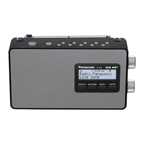
4 Specifications Power supply AC 230 V to 240 V, 50 Hz (For EB/GN) AC 230 V, 50 Hz (For EG) Battery DC 6 V (4 x R14/LR14, C) Power consumption 7 W (100 Hz, 6 Ω) Frequency range 87.50 MHz to 108.00 MHz (50 kHz steps) DAB/DAB+ BAND III 5A to 13F (174.928 MHz to 239.200 MHz) -
Page 10: Location Of Controls And Components
5 Location of Controls and Components Downloaded from www.Manualslib.com manuals search engine... -
Page 11: Self Diagnostic Mode
6 Self Diagnostic Mode This unit is equipped with features of service mode & doctor mode setting for checking the functions & reliability. Here is the procedures to enter into Self Diagnostic Mode. Step 1 : Turn on the unit. Step 2 : Press [MENU] button and turn the jog [TUNER/SELECT] to the left or right. -
Page 12: Disassembly And Assembly Instructions
7 Disassembly and Assembly Instructions • This section describes the disassembly and/or assembly procedures for all major printed circuit boards & main compo- nents for the unit. (You may refer to the section of “Main components and P.C.B Locations” as described in this service manual) •... -
Page 13: Disassembly Flow Chart
7.1. Disassembly flow chart The following chart is the procedure for disassembling the casing and inside parts for internal inspection when carrying out the ser- vicing. To assemble the unit, reverse the steps shown in the chart below. 7.2. Types of Screws Downloaded from www.Manualslib.com manuals search engine... -
Page 14: Main Parts Location Diagram
7.3. Main Parts Location Diagram Downloaded from www.Manualslib.com manuals search engine... -
Page 15: Disassembly Of Rear Cabinet Block
7.4. Disassembly of Rear Cabinet Step 2 : Lift up Rear Cabinet Block. Caution : Do not exert too much force as it may damage Block the wiring within. Step 3 : Release 3P Wire from the ribs. Step 4 : Detach it from the connector (CN901) on the Power Step 1 : Remove 5 screws. -
Page 16: Disassembly Of Power P.c.b., Battery (-) P.c.b. And Battery (+) P.c.b
7.5. Disassembly of Power P.C.B., Step 3 : Release the catch.. Battery (-) P.C.B. and Battery (+) P.C.B. • Refer to “Disassembly of Rear Cabinet Block” Step 1 : Remove 2 screws. Step 4 : Lift up the Power P.C.B., Battery (+) P.C.B.and Battery (-) P.C.B. -
Page 17: Disassembly Of D-Amp P.c.b
7.6. Disassembly of D-AMP P.C.B. Step 9 : Remove 2 screws. Step 10 : Upset the D-AMP P.C.B. as arrow shown. • Refer to “Disassembly of Rear Cabinet Block” Step 1 : Detach the 8P wire from connector (CN602) on D- AMP P.C.B.. -
Page 18: Disassembly Of Volume P.c.b
7.7. Disassembly of Volume P.C.B. Step 5 : Lift up the Main Chassis Block. • Refer to “Disassembly of Rear Cabinet Block” Step 1 : Remove the 2 Rotary Knobs. Step 6 : Remove 1 screw. Step 2 : Remove 2 screws. Step 3 : Remove 1 screw. -
Page 19: Disassembly Of Main P.c.b
7.8. Disassembly of Main P.C.B. Step 8 : Desolder the 5P wire at (P606B) on the Volume P.C.B.. Step 9 : Remove the Volume P.C.B.. • Refer to “Disassembly of Rear Cabinet Block” • Refer to (Step 1) - (Step 5) “Disassembly of Volume P.C.B.”. Step 1 : Detach the 22P FFC from connector (CN601) on the D-AMP P.C.B.. - Page 20 Step 3 : Remove 2 screws. Step 5 : Release the catches and remove the Front Button from the Main P.C.B.. Step 4 : Slightly lift up the Main P.C.B. as shown. Downloaded from www.Manualslib.com manuals search engine...
- Page 21 Step 6 : Desolder the wires (Black/White/Red). Step 9 : Lift up the Connector Cover. Step 7 : Desolder the wires (Blue/White). Step 10 : Detach the 14P FFC at connector (CN103) from the Step 8 : Desolder the 2P wire. Main P.C.B..
-
Page 22: Disassembly Of Top Key P.c.b And Headphone P.c.b
7.9. Disassembly of Top Key P.C.B Step 13 : Upset Main P.C.B.. Step 14 : Desolder the pins of Main P.C.B. shield. and Headphone P.C.B. Step 15 : Remove the Main P.C.B. shield. • Refer to “Disassembly of Rear Cabinet Block” •... - Page 23 Step 4 : Remove the Headphone P.C.B.. Step 6 : Remove the Support P.C.B.. Step 5 : Remove the Support P.C.B.. Step 7 : Lift up to remove the Top Button Block. Downloaded from www.Manualslib.com manuals search engine...
- Page 24 Step 8 : Remove 6 screws. Step 9 : Release 3 catches. Step 10 : Remove the Headphone P.C.B. and the Top Key P.C.B.. Downloaded from www.Manualslib.com manuals search engine...
-
Page 25: Disassembly Of Speaker (Sp1)
7.10. Disassembly of Speaker (SP1) • Refer to “Disassembly of Rear Cabinet Block” • Refer to (Step 1) - (Step 6) “Disassembly of Top Key P.C.B and Headphone P.C.B.”. Step 1 : Desolder the Speaker Wire. Step 2 : Remove 4 screws. Step 3 : Remove the Speaker (SP1) Downloaded from www.Manualslib.com... -
Page 26: Service Position
8 Service Position Note: For description of the disassembly procedures, see the Section 7 8.1. Checking of Power P.C.B. Step 2 : Lift up the Rear Cabinet Block. Step 3 : Release the 3P wire from the ribs. Step 1 : 1:Remove 5 screws. Downloaded from www.Manualslib.com manuals search engine... -
Page 27: Checking Of D-Amp P.c.b
8.2. Checking of D-AMP P.C.B. Step 4 : Place the Front and Rear Cabinet Block as shown in the diagram. • Refer to (Step 1) - (Step 3) of item 8.1. Step 5 : Remove 2 screws. Step 1 : Place the Front and Rear Cabinet Block as shown in the diagram. -
Page 28: Checking Of Main P.c.b. (Side A)
8.3. Checking of Main P.C.B. (Side Step 4 : Lift up the Main Chassis Block. • Refer to (Step 1) - (Step 3) of item 8.1. Step 1 : Remove 2 screws. Step 2 : Detach the 8P wire from connector (CN602) on the D- AMP P.C.B.. - Page 29 Step 7 : Slightly lift up the Main P.C.B.. Step 9 : Connect the 8P wire to connector (CN602) on the D- AMP P.C.B.. Step 8 : Release 4 catches and remove the Front Button. Step 10 : Main P.C.B (Side A) can be checked as diagram shown.
-
Page 30: Checking Of Main P.c.b. (Side B)
8.4. Checking of Main P.C.B. (Side Step 4 : Upset the Main P.C.B. and the LCD unit together on a support box. • Refer to item 8.3. Step 1 : Remove 2 screws. Step 5 : Desolder the pins of Main P.C.B. shield. Step 6 : Remove the Main P.C.B. - Page 31 Step 7 : Main P.C.B (Side B) can be checked as diagram shown. Downloaded from www.Manualslib.com manuals search engine...
- Page 32 Downloaded from www.Manualslib.com manuals search engine...
-
Page 33: Wiring Connection Diagram
9 Wiring Connection Diagram TOP KEY P.C.B. HEADPHONE P.C.B. BATTERY (-) P.C.B. HEADPHONE *P800 JK830 *P830 *ET901 DC 6V (TO SPEAKER) (4 x R14/LR14, C ) *P902B *JW901B *P606A *P603 *P604 CN601 CN602 *P606 *W25 *JW901A BATTERY (+) P.C.B. VOLUME P.C.B. DAMP P.C.B. - Page 34 Downloaded from www.Manualslib.com manuals search engine...
-
Page 35: Schematic Diagram
10 Schematic Diagram 10.1. Schematic Diagram Notes • Voltage and signal line (All schematic diagrams may be modified at any time with : +B Signal Line the development of new technology) Notes: S461: DISPLAY switch. S462: AUTOTUNE switch. S463: MENU switch. S464: ENTER switch. - Page 36 Downloaded from www.Manualslib.com manuals search engine...
-
Page 37: Main Circuit
10.2. MAIN CIRCUIT SCHEMATIC DIAGRAM -1 MAIN CIRCUIT : +B SIGNAL LINE JTAG IC203 C0FBBY000073 RX203 EXB28V221JX LB281 R281 R260 R-IN C281 SDIN VOUTR C123 6.04k SCLK J0JCC0000405 LRCK LB282 R282 C282 L-IN MCLK AOUTL FILT+ J0JCC0000405 R121 R201 4.7K 4.7K R120 R202... -
Page 38: D-Amp, Volume, Led & Headphone Circuit
10.3. D-AMP, VOLUME, LED & HEADPHONE CIRCUIT SCHEMATIC DIAGRAM - 2 D-AMP CIRCUIT : +B SIGNAL LINE ROD ANTENNA P606A* C609 C643 R606 MUTE RT_P JK600 VOLUME R602 RT_N CP101* 2.2K MAIN CIRCUIT CONTROL CIRCUIT RV_P CN602 (CP101*, CP103*) (P606B*) RV_N CP103* POWER KEY... -
Page 39: Top Key / Power / Battery (-) / Battery (+) Circuit
1.5K 2.2K 2.7K 3.9K 5.6K 8.2K KEY1 (CN602) IN SCHEMATIC DIAGRAM - 2 R810 R811 8.2K POWER CIRCUIT : +B SIGNAL LINE T901 (RTPN1I1E06-G...RF-D10EG) (RTPN1I1G07-G...RF-D10EB/GN) D904 C901 TRANSFORMER B0EAKM000117 0.01 D901 C904 D904 VA901 B0EAKM000117 ERZV05Z471CS 0.01 JK901 D902 AC IN... -
Page 40: Printed Circuit Board
11 Printed Circuit Board 11.1. MAIN P.C.B. MAIN P.C.B. (REPNT0073A) R443 R442 R441 C249 R444 IC504 X100 LB281 C281 R281 C264 QR503 CK251 RX203 LB282 R282 R201 C282 IC503 IC203 R555 C251 C561 R202 C273 C559 C247 LB203 C560 C244 R243 C552 R559... -
Page 41: Damp / Volume / Led / Headphone P.c.b
11.2. DAMP, VOLUME, LED & HEADPHONE P.C.B. DAMP P.C.B. (REPNT0074BA) VOLUME P.C.B. (REPNT0074BA) (TO SPEAKER) S822 P603* (TUNE/ P606A* C625 C626 SELECT) C653 P606* R633 P604* R641 Q613 R634 Q606 C623 Q607 IC600 QR608 R628 W27* C624 C630 S821 CN601 (VOLUME) 3711BF 3711BF... -
Page 42: Top Key / Power / Battery (-) / Battery (+) P.c.b
11.3. TOP KEY, POWER, BATTERY (-) & BATTERY (+) P.C.B. TOP KEY P.C.B. (REPNT0074BC) BATTERY (-) P.C.B. (REPNT0074BB) P800* S806 S805 S804 S803 S802 (MEMORY 10) (MEMORY 8) (MEMORY 6) (MEMORY 4) (MEMORY 2) S808 (MEMORY 7) R806 R805 R804 R803 R807 R808... -
Page 43: Appendix Information Of Schematic Diagram
12 Appendix Information of Schematic Diagram 12.1. Voltage Measurement & Waveform Chart Note: • Indicated voltage values are the standard values for the unit measured by the DC electronic circuit tester (high-impedance) with the chassis taken as standard. Therefore, there may exist some errors in the voltage values, depending on the internal impedance of the DC circuit tester. •... - Page 44 12.1.2. MAIN P.C.B. (2/3) REF NO. IC400 MODE RADIO ON STANDBY IC401 REF NO. MODE RADIO ON STANDBY IC402 REF NO. MODE RADIO ON STANDBY REF NO. IC403 MODE RADIO ON STANDBY REF NO. IC405 MODE RADIO ON STANDBY 12.6 IC501 REF NO.
- Page 45 12.1.3. MAIN P.C.B. (3/3) IC530 REF NO. MODE RADIO ON STANDBY 12.6 Q230 Q401 Q402 Q405 Q406 REF NO. MODE RADIO ON STANDBY 12.6 12.6 12.6 12.5 Q506 QR201 QR403 QR503 QR504 REF NO. MODE RADIO ON STANDBY 12.6 QR505 QR530 REF NO.
- Page 46 Downloaded from www.Manualslib.com manuals search engine...
-
Page 47: Exploded View And Replacement Parts List
S822 (LED P.C.B.) (VOLUME P.C.B.) CN205 (TO SOFTWARE UPDATE) *CP401 *CP101 (MAIN P.C.B.) *CP103 *CP402 CN103 RF-D10EB-K RF-D10EG/GN-K/W NOTE: " * " PART IS NOT SUPPLIED / REF IS FOR INDICATION ONLY. CABINET DRAWING Downloaded from www.Manualslib.com manuals search engine... - Page 48 13.1.2. Packaging ACCESSORIES BAG AC CORD AC CORD (FOR EB ONLY) (FOR GN ONLY) AC CORD (FOR EG ONLY) O/I BOOK RF-D10EB/EG/GN POLYFOAM (LEFT) RF-D10EB-K POLYFOAM (RIGHT) RF-D10EG/GN-K/W PACKAGING DRAWING Downloaded from www.Manualslib.com manuals search engine...
- Page 49 13.1.3. Mechanical Replacement Parts List Safety Ref. No. Part No. Part Name & QTY Remarks Description Safety Ref. No. Part No. Part Name & QTY Remarks RYKN0119D-K BACK CABINET EB-K Description ASS'Y 10-1 RKK0084-W1 BATTERY COVER EG/GN-W CABINET AND 10-1 RKK0084-1K BATTERY COVER EB/EG/...
- Page 50 Safety Ref. No. Part No. Part Name & QTY Remarks Description XTNR2+8CFJK SCREW XYN3+F25FN SCREW XTV3+14GFJK SCREW XTV3+14GFJ SCREW XTV3+10GFJ SCREW RGNN0183 NAME PLATE EB-K RGNN0184B NAME PLATE EG-W RGNN0184A NAME PLATE EG-K SPEAKERS RASN10PL12-G SPEAKER PACKING MATERI- RPGN00143 PACKING CASE EB-K RPGN00144 PACKING CASE...
-
Page 51: Electrical Replacement Parts List
13.2. Electrical Replacement Parts List Safety Ref. No. Part No. Part Name & QTY Remarks Description Safety Ref. No. Part No. Part Name & QTY Remarks IC505 C0DBEYY00271 IC (E.S.D) Description IC530 C0DBAYY01511 IC (E.S.D) IC600 C1AA00000829 IC (E.S.D) PRINTED CIR- IC601 C1BB00000947 IC (E.S.D) - Page 52 Safety Ref. No. Part No. Part Name & QTY Remarks Safety Ref. No. Part No. Part Name & QTY Remarks Description Description D902 B0EAKM000117 DIODE (E.S.D) JK830 RJJ37TK09 JK HEADPHONE D903 B0EAKM000117 DIODE (E.S.D) JK901 K2AA2B000014 AC INLET D904 B0EAKM000117 DIODE (E.S.D) D906 B0ACCK000005 DIODE...
- Page 53 Safety Ref. No. Part No. Part Name & QTY Remarks Safety Ref. No. Part No. Part Name & QTY Remarks Description Description R402 ERJ2GEYJ101V 100 1/16W C105 F1G1H102A459 1000pF R403 ERJ2GEYJ101V 100 1/16W C106 F1G1H102A459 1000pF R404 ERJ2GEYJ101V 100 1/16W C107 F1G1A104A012 0.1uF R405...
- Page 54 Safety Ref. No. Part No. Part Name & QTY Remarks Safety Ref. No. Part No. Part Name & QTY Remarks Description Description C278 F1J0J2260004 22uF 6.3V C634 F1H1C225A065 2.2uF C281 F1H0J4750004 4.7uF 6.3V C635 F2A1C222A321 2200uF C282 F1H0J4750004 4.7uF 6.3V C636 RCA0JKA470BT 47 6.3V...
Need help?
Do you have a question about the RF-D10EG and is the answer not in the manual?
Questions and answers