Table of Contents
Advertisement
Quick Links
Advertisement
Chapters
Table of Contents

Related Manuals for LG CM9730


Summary of Contents for LG CM9730
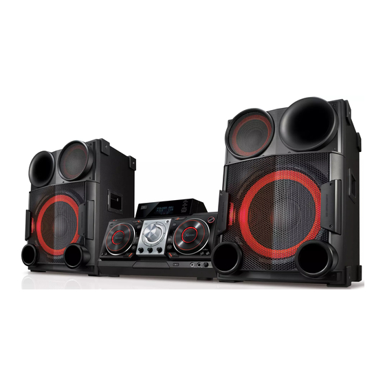
- Page 1 Internal Use Only Website http://biz.lgservice.com SUPER POWER MINI HI-FI SYSTEM SERVICE MANUAL MODEL: CM9730 (CM9730, NS9730F) CAUTION BEFORE SERVICING THE UNIT, READ THE “SAFETY PRECAUTIONS” IN THIS MANUAL. JANUARY...
- Page 2 CONTENTS SECTION 1 ..GENERAL SECTION 2 ..CABINET & MAIN CHASSIS SECTION 3 ..ELECTRICAL SECTION 4 ..REPLACEMENT PARTS LIST...
-
Page 3: Table Of Contents
SECTION 1 SUMMARY CONTENTS SERVICING PRECAUTIONS ........................1-3 ESD PRECAUTIONS ..........................1-5 HIDDEN KEY MODE ........................... 1-6 SERVICE INFORMATION FOR EEPROM ..................1-7 PROGRAM UPGRADE GUIDE ....................... 1-8 SPECIFICATIONS ............................1-9... -
Page 4: Servicing Precautions
SERVICING PRECAUTIONS NOTES REGARDING HANDLING OF THE PICK-UP 1. Notes for transport and storage 1) The pick-up should always be left in its conductive bag until immediately prior to use. 2) The pick-up should never be subjected to external pressure or impact. Storage in conductive bag Drop impact 2. - Page 5 NOTES REGARDING COMPACT DISC PLAYER REPAIRS 1. Preparations 1) Compact disc players incorporate a great many ICs as well as the pick-up (laser diode). These components are sensitive to, and easily affected by, static electricity. If such static electricity is high voltage, components can be damaged, and for that reason components should be handled with care.
-
Page 6: Esd Precautions
ESD PRECAUTIONS Electrostatically Sensitive Devices (ESD) Some semiconductor (solid state) devices can be damaged easily by static electricity. Such components commonly are called Electrostatically Sensitive Devices (ESD). Examples of typical ESD devices are integrated circuits and some field-effect transistors and semiconductor chip components. The following techniques should be used to help reduce the incidence of component damage caused by static electricity. -
Page 7: Hidden Key Mode
HIDDEN KEY MODE Push both Front key and RCU key to activate it for 5 seconds. 1. Disc Lock On/Off (CD Function Only Active) Front Key : STOP RCU Key : STOP 2. Check Version and Option code Front Key : STOP RCU Key : PLAY/PAUSE You can change [Audio MCU Version <->... -
Page 8: Service Information For Eeprom
FLD ‘OP-0…. Move to appropriate position and make changes with remote control. /■ , REPEAT ) Press STOP key * MODEL.SUFFIX <A> CM9730-DB.DDEULLK <B> CM9730-FB.DARELLS FLD ‘write ok’ <C> CM9730-FB.DGHALLS Remote control ‘ ’ + Front ‘STOP’ push same timing. -
Page 9: Program Upgrade Guide
PROGRAM UPGRADE GUIDE 1. Check the download fi le name. MICOM Mpeg File Name CM9730_”version”.HEX HE004_”version”.BIN EQ_PRG.BIN * There is the Update File only in the USB storage. 2. Copy the download fi le to the USB storage. 3. Insert the USB storage on USB1 or USB2 Function. 4. -
Page 10: Specifications
SPECIFICATIONS • GENERAL Power requirements Refer to the main label. Power consumption Refer to the main label. Dimensions (W x H x D) 542 x 308 x 421 mm Net Weight (Approx.) 9.85 kg Operating temperature 5 °C to 35 °C (41 °F to 95 °F) Operating humidity 5 % to 90 % Bus Power Supply... - Page 11 MEMO 1-10...
- Page 12 SECTION 2 CABINET & MAIN CHASSIS CONTENTS EXPLODED VIEWS ............................. 2-3 1. CABINET AND MAIN FRAME SECTION (CM9730) ................2-3 2. MECHANISM DECK SECTION (DP17T) ....................2-5 3. WOOFER SECTION (NS9730F) ......................2-7 4. PACKING ACCESSORY SECTION ......................2-9...
- Page 13 MEMO...
-
Page 14: Exploded Views
EXPLODED VIEWS NOTES) THE EXCLAMATION POINT WITHIN AN EQUILATERAL TRIANGLE IS INTENDED 1. CABINET AND MAIN FRAME SECTION (CM9730) TO ALERT THE SERVICE PERSONNEL TO THE PRESENCE OF IMPORTANT SAFETY INFORMATION IN SERVICE LITERATURE. A44C CABLE1 CABLE8 CABLE4 MULTI VOLUME... -
Page 15: Mechanism Deck Section (Dp17T)
2. MECHANISM DECK SECTION (DP17T) 1439 1002 A001 1005 1001 1026 1003 1004 1030 1024 1437 1437 1024 1024 1012 1049 1437 1024 1015 1016 1013 1020 1011 A006 1019 1043 1018 1045 A005 1439... -
Page 16: Woofer Section (Ns9730F)
NOTES) THE EXCLAMATION POINT WITHIN AN EQUILATERAL TRIANGLE IS INTENDED 3. WOOFER SECTION (NS9730F) TO ALERT THE SERVICE PERSONNEL TO THE PRESENCE OF IMPORTANT SAFETY INFORMATION IN SERVICE LITERATURE. A61L A60L A62L A61R A60R A62R LED Signal Cable A63L A63R... -
Page 17: Packing Accessory Section
MEMO 4. PACKING ACCESSORY SECTION 801 Owner’s Manual 900 Remote Control 825 FM Wire Antenna 808 Battery 803 Packing 804 Bag 803 Packing 802 Box... - Page 18 SECTION 3 ELECTRICAL CONTENTS ONE POINT REPAIR GUIDE ..........................3-2 1. NO POWER ............................3-2 2. NO BOOTING WHEN POWER ON THE SET ..................3-4 3. VFD IS NOT DISPLAYED WHEN POWER ON THE SET ..............3-5 4. NO BOOTING IN CD/USB FUNCTION ....................3-6 5.
-
Page 19: One Point Repair Guide
ONE POINT REPAIR GUIDE 1. NO POWER If the unit doesn’t work by no power problem, repair the set according to the following guide. 1-1. FUSE / BRIDGE DIODE / THERMISTOR 1-1-1. Solution Please check and replace F901, BD901, TH900, TH901, TH902 on SMPS board. 1-1-2. - Page 20 ONE POINT REPAIR GUIDE NO POWER If the unit doesn’t work by no ±PVDD problem, repair the set according to the follow- ing guide. 1-2. NO AMP POWER 1-2-1. Solution Please check and replace F911, Q911 ~ Q914 on SMPS board. 1-2-2.
-
Page 21: No Booting When Power On The Set
ONE POINT REPAIR GUIDE 2. NO BOOTING WHEN POWER ON THE SET The set doesn’t work when press the power button on the front board or the remote control. 2-1. FLASH MEMORY (IC101) 2-1-1. Solution Please check and replace IC101 on MAIN board. 2-1-2. -
Page 22: Vfd Is Not Displayed When Power On The Set
ONE POINT REPAIR GUIDE 3. VFD IS NOT DISPLAYED WHEN POWER ON THE SET When power on the set, any icons or characters on VFD are not displayed. 3-1. VFD (DIG301) 3-1-1. Solution Please check and replace DIG301 on FRONT board. 3-1-2. - Page 23 ONE POINT REPAIR GUIDE 4. NO BOOTING IN CD/USB FUNCTION After you turn on power key and displayed message in the following order (HELLO --> VOL XX --> CD or USB) on VFD, it will not display other message on VFD, and it will not boot-up normally. 4-1.
-
Page 24: No Booting In Cd/Usb Function
ONE POINT REPAIR GUIDE NO BOOTING IN CD/USB FUNCTION After you turn on power key and displayed message in the following order (HELLO --> VOL XX --> CD or USB) on VFD, it will not display other message on VFD, and it will not boot-up normally. 4-2. - Page 25 ONE POINT REPAIR GUIDE NO BOOTING IN CD/USB FUNCTION After you turn on power key and displayed message in the following order (HELLO --> VOL XX --> CD or USB) on VFD, it will not display other message on VFD, and it will not boot-up normally. 4-3.
- Page 26 ONE POINT REPAIR GUIDE NO BOOTING IN CD/USB FUNCTION After you turn on power key and displayed message in the following order (HELLO --> VOL XX --> CD or USB) on VFD, it will not display other message on VFD, and it will not boot-up normally. 4-4.
- Page 27 ONE POINT REPAIR GUIDE NO BOOTING IN CD/USB FUNCTION After you turn on power key and displayed message in the following order (HELLO --> VOL XX --> CD or USB) on VFD, it will not display other message on VFD, and it will not boot-up normally. 4-5.
- Page 28 ONE POINT REPAIR GUIDE 5. NO OPERATION OF MD When no sound output in the CD function, you can not listen to music reading data from a CD disc if the servo motors in MD don’t work. This step is for checking the SPINDLE MOTOR among them.
-
Page 29: No Operation Of Md
ONE POINT REPAIR GUIDE NO OPERATION OF MD When no sound output in the CD function, you can not listen to music reading data from a CD disc if the servo motors in MD don’t work. This step is for checking the SLED MOTOR among them. - Page 30 ONE POINT REPAIR GUIDE NO OPERATION OF MD When no sound output in the CD function, you can not listen to music reading data from a CD disc if the servo motors in MD don’t work. This step is for checking the TRAY OPEN/CLOSE MOTOR among them.
- Page 31 ONE POINT REPAIR GUIDE NO OPERATION OF MD When no sound output in the CD function, you can not listen to music reading data from a CD disc if the pickup module in MD doesn’t work. This step is for checking the LASER TRACKING ACTUATOR.
- Page 32 ONE POINT REPAIR GUIDE NO OPERATION OF MD When no sound output in the CD function, you can not listen to music reading data from a CD disc if the pickup module in MD doesn’t work. This step is for checking the LASER FOCUSING ACTUATOR.
- Page 33 ONE POINT REPAIR GUIDE 6. NO SOUND There is no sound output in the CD FUNCTION, repair the set according to the follow- ing guide. 6-1. IN THE CD FUNCTION 6-1-1. Solution Please check and replace IC501, IC600 on MAIN board. 6-1-2.
-
Page 34: No Sound
ONE POINT REPAIR GUIDE NO SOUND There is no sound output in the USB FUNCTION, repair the set according to the fol- lowing guide. 6-2. IN THE USB FUNCTION 6-2-1. Solution Please check and replace IC501, IC504 on MAIN board & IC3U01 on USB board. 6-2-2. - Page 35 ONE POINT REPAIR GUIDE NO SOUND There is no sound output in the AUX FUNCTION, repair the set according to the fol- lowing guide. 6-3. IN THE AUX FUNCTION 6-3-1. Solution Please check and replace IC202 on MAIN board. 6-3-2. How to troubleshoot (Countermeasure) 1) Check AUX_L/R signals to IC202 (Pin7, 8).
- Page 36 ONE POINT REPAIR GUIDE NO SOUND There is no sound output in the PORT. IN FUNCTION, repair the set according to the following guide. 6-4. IN THE PORT. IN FUNCTION 6-4-1. Solution Please check and replace IC202 on MAIN board. 6-4-2.
- Page 37 ONE POINT REPAIR GUIDE NO SOUND There is no sound output in the TUNER FUNCTION, repair the set according to the following guide. 6-5. IN THE TUNER FUNCTION 6-5-1. Solution Please check and replace IC202, TU801 on MAIN board. 6-5-2. How to troubleshoot (Countermeasure) 1) Check if TUNER_LR is entered from Pin1 &...
- Page 38 ONE POINT REPAIR GUIDE NO SOUND There is no sound output in the MIC IN FUNCTION, repair the set according to the following guide. 6-6. IN THE MIC IN FUNCTION 6-6-1. Solution Please check and replace IC508, IC506 on MAIN board. 6-6-2.
- Page 39 ONE POINT REPAIR GUIDE NO SOUND There is no sound output in the BLUETOOTH FUNCTION, repair the set according to the following guide. 6-7. IN THE BLUETOOTH FUNCTION 6-7-1. Solution Please check and replace IC501 on MAIN board and Bluetooth module on front panel. 6-7-2.
-
Page 40: Audio Output Is Small Or No Audio Output
ONE POINT REPAIR GUIDE 7. AUDIO OUTPUT IS SMALL OR NO AUDIO OUTPUT Audio signal output is small or not. when you power on the Middle Power Mini System. 7-1. IC700 ~ IC706 & IC708 7-1-1. Solution Please check and replace IC700 ~ IC706 & IC708 on MAIN board. 7-1-2. -
Page 41: No Power On (Standby Led Is Blinking)
ONE POINT REPAIR GUIDE 8. NO POWER ON (STANDBY LED IS BLINKING) It doesn’t turn on, and blinks standby LED(Red). 8-1. AMP FETs 8-1-1. Solution Please check and replace Q700 ~ Q705, Q708, Q709, Q714, Q716, Q719 ~ Q724 on MAIN board. 8-1-2. -
Page 42: Speaker No Audio
ONE POINT REPAIR GUIDE 9. SPEAKER NO AUDIO Speaker No Audio 9-1. AMP IC 9-1-1. Solution Please check and replace the component on MAIN board. 9-1-2. How to troubleshoot (Countermeasure) 1) Check supply voltage of AMP(CN700, CN701) & PWM signal Normal Supply voltage and signal Check AMP IC. -
Page 43: Electrical Troubleshooting Guide
ELECTRICAL TROUBLESHOOTING GUIDE 1. POWER SUPPLY ON SMPS BOARD No output 5.6 VA Replace F901 (same fuse). F901 normal? Replace BD901. BD901 normal? Is the VCC D960, D961 normal? (11 V ~ 25 V) supplied to IC901 Pin4? Power line of MAIN PCB is short. Check or replace D960, D961. - Page 44 ELECTRICAL TROUBLESHOOTING GUIDE No -5 V Is the R965 normal? Check or replace R965, D959. VCC -7 VA supplied to IC953 Pin2? Check or replace Q951. Is there ‘H’ signal at Q953 Check P_CTL from μ-com. Base? Check or replace Q953, Q957. Or check line of MAIN PCB is short or not.
- Page 45 ELECTRICAL TROUBLESHOOTING GUIDE No output AMP gate line Is the VCC R952 normal? 13 VA supplied to IC952 Check or replace R952. Pin1, 3? Check and replace IC952. Check or replace D951, D952. Or check line of MAIN PCB is short or not. 3-28...
- Page 46 ELECTRICAL TROUBLESHOOTING GUIDE No AMP output Is the PFC P.CTL OK? C904, C905 voltage Check PFC P.CTL from μ-com. about 380 V? Is the VCC 12V supplied to Replace D908, Q955, PC903. IC904 Pin16? Check or replace IC904, Q907 ~ Q910. AMP P.CTL F911 normal? Check AMP P.CTL from μ-com.
-
Page 47: System Part
ELECTRICAL TROUBLESHOOTING GUIDE 2. SYSTEM PART Power on. CN301 “HELLO” cable connection Display on FLD Check 17p FFC cable. CN301 pin1, 3, 5 Check SMPS board. power OK? CN301 Pin9, 10, 11 data signal Check MAIN board. Q301, 303, 304 grid voltage OK? Replace DIG301. - Page 48 ELECTRICAL TROUBLESHOOTING GUIDE Power on. CN301 “HELLO” cable connection Display on FLD Check 17p FFC cable. CN301 Pin1, 3, 5 power Check SMPS board. CN301 Pin9, 10, 11 data signal Check MAIN board. Q301, 303, 304 Replace DIG301. grid voltage OK? CN3V01 Volume LED (LD3V31 ~ LD3V49) Jog LED...
-
Page 49: No Audio Part
ELECTRICAL TROUBLESHOOTING GUIDE 3. NO AUDIO PART CD FUNCTION Is motor_open/ close OK? LOAD +- OK? disc insert? (IC408 Pin9,10) Check IC501. Is motor impedance Check Loading motor. about 12 Ω? Check IC408. Focusing/ OPU driving Tracking/ Sled signal Disc reading OK? (Focusing &... - Page 50 ELECTRICAL TROUBLESHOOTING GUIDE USB play IC501 Check IC501. Pin16, 18 USB_HUB_D output signal OK? IC3U01 When insert USB power +5 VU Replace IC3U01. USB, IC504 Pin1, 2, 3, 4 USB_D signal OK? IC202 Pin7,8 AUX input signal Check audio cable. IC202 Check IC501.
- Page 51 ELECTRICAL TROUBLESHOOTING GUIDE POT. IN IC202 Pin21,22 POT. IN input signal Check MIC board. IC202 Check IC501. Pin42,43,44 I2S input signal IC202 Replace IC202. Pin41 ADC data output signal TUNER TU101 IC202 TUNER_L/R output Pin23,24 TUNER_L/R input Check +3.3 V of TU101. signal OK? signal OK? IC202...
- Page 52 ELECTRICAL TROUBLESHOOTING GUIDE IC501 Pin82, 83, 84 I2S data output Check IC501. signal OK? IC501 pin 85 I2S data signal Check IC501. IC600 Replace IC600. PWM data output signal 3-35...
- Page 53 ELECTRICAL TROUBLESHOOTING GUIDE IC600 IC600 Pin28,29,35,36 FL/FR± Pin26,27,31,32 SWL/SWR± signal OK? signal OK? Check IC600. Check IC600. IC601, IC603, IC602 FL/FR audio signal IC604 SWL/SWR audio signal OK? Check IC601,IC602 Check IC603,IC604 Pin13 of Pin13 of IC702, IC700,IC701,IC704,IC705 FL/FR IC703,IC706,IC708 SWL/SWR audio signal OK? audio signal OK? Check IC700,...
-
Page 54: No Lighting (Woofer Speaker)
ELECTRICAL TROUBLESHOOTING GUIDE 4. NO LIGHTING (WOOFER SPEAKER) CD/ USB play CN803, CN804 Pin3,7 I2C signal Check IC501. CN803, CN804 Pin8 +12 V Check SMPS board. CN803, Check IC605. Replace IC605. CN804 Pin1 +3.3 V Check Woofer SPK. Check SMPS board. 3-37... -
Page 55: Waveforms
WAVEFORMS 1. WAVEFORM OF SERVO Figure 1-1. CD-16M Figure 1-2. SERVO-FE, TE, FOD, RF (IC407 Pin31) (IC407 Pin61, 62, 63 / IC408 Pin1) 3-38... - Page 56 2. WAVEFORM OF MOTOR DRIVE Figure 2-1. SP- & SP+ for driving SPINDLE motor Figure 2-2. SL- & SL+ for driving SPINDLE motor (IC408 Pin17, 18) (IC408 Pin11, 12) MOT_OPEN LO+(RED) MOT_CLOSE Figure 2-3. LO- & LO+ for driving Tray motor (IC408 Pin9, 10) 3-39...
- Page 57 3. WAVEFORM OF AUDIO SIGNAL AUDIO_L LRCK DATA AUDIO_R Figure 3-1. (IC501 Pin83, 84, 85) Figure 3-2. AUDIO_L/R 4. WAVEFORM OF ADC 5. WAVEFORM OF USB LRCK Figure 4. ADC I2S Figure 5. USB D+/D- (IC202 Pin42, 43, 44) (CN502 Pin1, 2 & Pin9, 10) 3-40...
- Page 58 6. WAVEFORM OF CRYSTAL 7. WAVEFORM OF VFD GRID CURRENT DRIVER CH1:R327(TP304) CH2:Q301 Emitter Figure 6. 12 MHz Crystal Figure 7. (IC501 Pin27, 28) 3-41...
- Page 59 MEMO 3-42...
-
Page 60: Wiring Diagram
WIRING DIAGRAM 3-43 3-44... -
Page 61: Block Diagrams
BLOCK DIAGRAMS 1. SMPS BLOCK DIAGRAM 3-45 3-46... -
Page 62: Main System Block Diagram
2. MAIN SYSTEM BLOCK DIAGRAM 16.9344MHz 15pF IC407 BU9543KV USB1 USB2 SPDO/SLDO/FOD/TRD P/UP P/UP RF+ SERVO Bluetooth B B B luetooth h h h 12MHz IC408 IC504 S3053 USB2512B MOT_MUTE/CLOSE/OPEN BT_TX USB HUB Motor Drive BT_RX PT_L/R OP_SW,CL_SW Portable USB_HUB_DP/DN IC200 AUX_L/R USB_RESET... -
Page 63: Circuit Diagrams
BE MODIFIED OR ALTERED WITHOUT PERMISSION FROM THE ACTUAL CIRCUIT USED. THIS WAY, 1. SMPS #1 CIRCUIT DIAGRAM FROM THE LG CORPORATION. ALL COMPONENTS IMPLEMENTATION OF THE LATEST SAFETY AND SHOULD BE REPLACED ONLY WITH TYPES PERFORMANCE IMPROVEMENT CHANGES INTO IDENTICAL TO THOSE IN THE ORIGINAL CIRCUIT. -
Page 64: Smps #2 Circuit Diagram
2. SMPS #2 CIRCUIT DIAGRAM Warning Parts that are shaded are critical with respect to risk of fire or electrical shock. SMPS #2 EAX64780401-SD_9.1.7 2012. 09. 12 3-51 3-52... -
Page 65: Main - Micom Circuit Diagram
3. MAIN - MICOM CIRCUIT DIAGRAM MAIN - MICOM EAX64843601-SD_4.1.4 2012. 09. 12 3-53 3-54... -
Page 66: Main - Pwm Circuit Diagram
4. MAIN - PWM CIRCUIT DIAGRAM MAIN - PWM EAX64843601-SD_4.1.4 2012. 09. 12 3-55 3-56... -
Page 67: Main - Amp Circuit Diagram
5. MAIN - AMP CIRCUIT DIAGRAM MAIN - AMP EAX64843601-SD_4.1.4 2012. 09. 12 3-57 3-58... -
Page 68: Main - Dsp Circuit Diagram
6. MAIN - DSP CIRCUIT DIAGRAM 12 14 : WAVEFORM NUMBER MAIN - DSP EAX64843601-SD_4.1.4 2012. 09. 12 3-59 3-60... -
Page 69: Main - Rf Servo Circuit Diagram
7. MAIN - RF SERVO CIRCUIT DIAGRAM MAIN - RF SERVO : WAVEFORM NUMBER EAX64843601-SD_4.1.4 2012. 09. 12 3-61 3-62... -
Page 70: Main - Adc Circuit Diagram
8. MAIN - ADC CIRCUIT DIAGRAM 17 16 15 : WAVEFORM NUMBER MAIN - ADC EAX64843601-SD_4.1.4 2012. 09. 12 3-63 3-64... -
Page 71: Vfd Circuit Diagram
9. VFD CIRCUIT DIAGRAM : WAVEFORM NUMBER EAX64800501-SD_3.1.3 2012. 09. 12 3-65 3-66... -
Page 72: Main Volume Circuit Diagram
10. MAIN VOLUME CIRCUIT DIAGRAM MAIN VOLUME EAX64800401-SD_4.1.4 2012. 09. 12 3-67 3-68... -
Page 73: Mic Circuit Diagram
11. MIC CIRCUIT DIAGRAM EAX64800601-SD_4.1.4 2012. 09. 12 3-69 3-70... -
Page 74: Multi Jog Volume Circuit Diagram
12. MULTI JOG VOLUME CIRCUIT DIAGRAM MULTI JOG VOLUME EAX64870401-SD_5.1.5 2012. 09. 12 3-71 3-72... -
Page 75: Usb Circuit Diagram
13. USB CIRCUIT DIAGRAM EAX64781501-SD_5.1.5 2012. 09. 12 3-73 3-74... -
Page 76: Aux / Tuner / Speaker Light Jack Circuit Diagram
14. AUX / TUNER / SPEAKER LIGHT JACK CIRCUIT DIAGRAM AUX/ TUNER/ SPK LIGHT JACK EAX64800701-SD_5.1.5 2012. 09. 12 3-75 3-76... -
Page 77: Speaker Led_Main Circuit Diagram
15. SPEAKER LED_MAIN CIRCUIT DIAGRAM SPK LED_MAIN EAX65023001-SD_3.1.3 2012. 09. 12 3-77 3-78... -
Page 78: Speaker Led Circuit Diagram
16. SPEAKER LED CIRCUIT DIAGRAM SPK LED EAX65022901-SD_3.1.3 2012. 09. 12 3-79 3-80... -
Page 79: Circuit Voltage Chart
CIRCUIT VOLTAGE CHART 1. ICs PIN NO. SPEC. VOLTAGE PIN NO. SPEC. VOLTAGE PIN NO. SPEC. VOLTAGE IC Sym IC Name / Type Vcc/Vdd IC Sym IC Name / Type Vcc/Vdd IC100 (EEPROM) IC605 (LDO) LC87F5NC8A(SANYO) Spec: LM37102D Spec: 3.3VA 3.471 3.7VA 3.71... - Page 80 2. CAPACITORS 3. CONNECTORS Location Spec Voltage[V] Location Spec Voltage[V] Location Spec Voltage[V] PIN NO. DESCRIPTION VOLTAGE PIN NO. DESCRIPTION VOLTAGE PIN NO. DESCRIPTION VOLTAGE DSP Block C485 220uF/16V C765 470uF/50V -39.7 Harness Board IN, 15P, 2.5mm DGND /RST C525 47uF/16V 3.27 C492...
- Page 81 CONNECTORS PIN NO. DESCRIPTION VOLTAGE PIN NO. DESCRIPTION VOLTAGE PIN NO. DESCRIPTION VOLTAGE PIN NO. DESCRIPTION VOLTAGE HARNESS, 10P, 2.00mm EQ_M_B T(-) +PVDD_R 39.6 USB - MAIN DGND F(-) CN3U1 EQ_T_A SW PDIC 5.06 PGND_R EQ_T_B DGND CD LD -PVDD_R -39.7 DGND FFC, 17P, 1.25mm...
-
Page 82: Printed Circuit Board Diagrams
PRINTED CIRCUIT BOARD DIAGRAMS NOTE) Warning Parts that are critical with respect to risk 1. SMPS P.C.BOARD of fire or electrical shock. 3-87 3-88... -
Page 83: Main P.c.board
2. MAIN P.C.BOARD (TOP VIEW) 3-89 3-90... - Page 84 MAIN P.C.BOARD (BOTTOM VIEW) 3-91 3-92...
-
Page 85: Vfd P.c.board
3. VFD P.C.BOARD 3-93 3-94... -
Page 86: Main Volume P.c.board
4. MAIN VOLUME P.C.BOARD 5. MIC P.C.BOARD 3-95 3-96... -
Page 87: Jog P.c.board
6. JOG P.C.BOARD 7. USB P.C.BOARD 8. TUNER P.C.BOARD 3-97 3-98... -
Page 88: Speaker Led_Main P.c.board
9. SPEAKER LED_MAIN P.C.BOARD (TOP VIEW) (BOTTOM VIEW) 10. SPEAKER LED P.C.BOARD (TOP VIEW) (BOTTOM VIEW) 3-99 3-100... - Page 89 MEMO MEMO 3-101 3-102...
Need help?
Do you have a question about the CM9730 and is the answer not in the manual?
Questions and answers