Table of Contents
Advertisement
Quick Links
DRS4 Evaluation Board User's Manual
DRS4 Evaluation Board
User's Manual
Board Revision 5
as of January 2014
Last revised: April 27, 2016
Stefan Ritt
Paul Scherrer Institute
CH-5232 Villigen PSI
Switzerland
Email:
stefan.ritt@psi.ch
Phone: +41 56 310 3728
Please check for possible updates of this manual under http://www.psi.ch/drs/documentation
Advertisement
Table of Contents

Related Manuals for PSI DRS4

Summary of Contents for PSI DRS4
-
Page 1: Board Revision
User’s Manual Board Revision 5 as of January 2014 Last revised: April 27, 2016 Stefan Ritt Paul Scherrer Institute CH-5232 Villigen PSI Switzerland Email: stefan.ritt@psi.ch Phone: +41 56 310 3728 Please check for possible updates of this manual under http://www.psi.ch/drs/documentation... -
Page 2: Revision History
DRS4 Evaluation Board User’s Manual Revision History Date Modification 2 March 09 Initial Revision 27 April 09 Mention input range, added timing calibration description 3 Aug. 09 Added LED description 12 July 10 Updated documentation for evaluation board V3 12 Sept. 10 Added maximum input voltage 16. -
Page 3: Table Of Contents
4.2. Analog Input ....................... 28 4.3. Control Voltages ......................29 4.4. ADC Clock ......................... 29 4.5. Calibration ........................29 5. DRS4 Evaluation Board V5 Schematics ................30 6. DRS4 Evaluation Board V5 Bill of Materials ..............37 Page 3 of 43... -
Page 4: Introduction
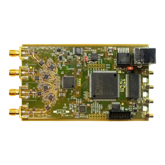
Two reference voltages are generated by the on-board 16-bit DAC to measure the offset and gain of all DRS4 storage cells for calibration. The four analog inputs are AC coupled and have a input range of 1 V peak-to- ®... - Page 5 DRS4 Evaluation Board User’s Manual For trigger purposes and inter-board synchronization, four MCX connectors are available, which can be seen on the right side of Figure 1. The Trigger IN works as an external trigger much like the one of an oscilloscope. The electrical standard is 5V TTL. Although a 50 Ω...
-
Page 6: Leds
DRS4 Evaluation Board User’s Manual 1.2. LEDs The DRS4 evaluation board is equipped with three LEDs. They are operated by the micro controller and the FPGA and have following meaning: Meaning This LED becomes green when the on-board micro-controller booted Blue successfully. -
Page 7: Firmware Description
Both the Windows and the Linux distribution contain a subdirectory “firmware” which contains the FPGA and Microcontroller firmware for the DRS4 Evaluation Board. The FPGA firmware is written in pure VHDL, thus making it easy to port it to other FPGA devices such ®... - Page 8 DRS4 Evaluation Board User’s Manual The FPGA firmware implements a set of control and status registers, through which the DRS4 can be controlled and read out. The mapping of the control registers is as follows: Ofs. Name Comment 0x00 start_trig Write a "1"...
-
Page 9: Installation
0x3a 15..0 scaler_1lo All registers are implemented as 32-bit registers, so they can be mapped easily into some VME address space for example if one decides to build a VME board containing the DRS4. 2. Installation 2.1. Windows XP ®... - Page 10 DRS4 Evaluation Board User’s Manual Then you can select the installation directory: After the installer has finished, you can connect the DRS4 Evaluation Board to the Computer: Now you will see the “Found New Hardware” dialog: Page 10 of 43...
- Page 11 DRS4 Evaluation Board User’s Manual Where you can click “Install the software automatically” and then click “Next”. After successful installation of the driver, you will see the following window: And a new group in your Start Menu: The software comes with two applications, a command line interface and an oscilloscope.
-
Page 12: Windows 7
Please select “Install this driver software anyway” to install the driver. After the software has been installed, you can connect the DRS4 Evaluation Board to the computer. The driver installation should then start automatically and you will see this notification: When this has finished, you can start the “drscl”... - Page 13 Click “No” on the next page asking to connect to Windows Update, then select “Install the software automamtically”: This will update the USB driver for the DRS4 board correctly. The board will now be listed under “libusb (WinUSB) devices” instead of “LibUSB-Win32 Devices”.
-
Page 14: Linux
-DHAVE_LIBUSB -c src/mxml.c . . . Now you can connect the DRS4 board to the PC. On systems where the “lsusb” tool is installed, one should be able to find the DRS4 evaluation board after connecting it with following command: [/usr/local/drs-1.0]$ /sbin/lsusb -d 04b4:1175 –v... - Page 15 DRS4 Evaluation Board User’s Manual If the board is correctly recognized, one can access it with the command line program. Under most Linux distributions however, only the “root” user can directly access USB devices. Some systems can be configured to allow non-root access via the “udev” system, but the exact instructions vary from distribution to distribution and can therefore not be given here.
-
Page 16: Macintosh Osx
A more convenient way is however to install the pre-compiled binary DRSOsc program. Simply download DRS Oscilloscope.dmg from http://www.psi.ch/drs/download, click on it and drag the DRSOsc icon into the Application folder. The libusb library is already compiled into the executable so does not need to be installed separately, unless one wants to compile the programs from the tar ball. -
Page 17: Running The Board
Clicking on „DRS Command Line Interface“ (Windows) or entering “drscl” (Linux) will start a simple application which connects to the DRS4 Evaluation Board. If it finds the board, it displays the board serial number and the firmware revision as on the following screen shot: Now you are ready to issue your first command “info”... -
Page 18: Oscilloscope Application "Drsosc
3.2. Oscilloscope application “DRSOsc” The second application is an oscilloscope-like program, which connects to the DRS4 board and works pretty much like a normal oscilloscope. You can select the trigger mode, trigger level and trigger source, which can also be a logical combination of channels. You enable a channel by clicking on the number “1”... - Page 19 0.2 ns by up to ±100 ps, and the integral timing nonlinearity adds up to almost 0.4 ns, which is typical for the DRS4 chip. Since transistor parameters have normally gradients over the chip wafer, SCA chips are usually “faster” on one side than on the other.
- Page 20 DRS4 Evaluation Board User’s Manual This calibration data both for voltage and timing is then stored in the EEPROM on the evaluation board, from where it is obtained each time the oscilloscope gets started. This assures that a board is calibrated even when used on different computers. Note however that the timing calibration is only valid for one individual sampling speed.
- Page 21 DRS4 Evaluation Board User’s Manual For test purposes, an internal 100 MHz reference clock signal can be connected to all channels via the “Config” menu: The effect of the timing calibration can be tested by turning the timing calibration on and off via the “Apply Timing Calibration”...
- Page 22 After the board serial number there is an entry of the Trigger Cell. This is the DRS4 memory cell which received the trigger, which can normally be ignored.
- Page 23 DRS4 Evaluation Board User’s Manual data was recorded. It might be a single channel (CHN1) or all four channels (CHN1-CHN4). Please note that the XML format requires more hard disk space compared to the binary format and takes also more CPU power to be written, so the maximum data rate is limited.
- Page 24 If the array dt [1024] contains the effective bin widths of a channel ch of the DRS4 chip obtained from the binary file, the time t belonging to sample i can be calculated using the trigger cell tcell as follows: i−1...
- Page 25 DRS4 Evaluation Board User’s Manual Word Byte 0 Byte 1 Byte 2 Byte 3 Contents File header, Byte 3 = version ‘D’ ‘R’ ‘S’ ‘2’ Time Header ‘T’ ‘I’ ‘M’ ‘E’ Board serial number ‘B’ ‘#’ Board number ‘C’ ‘0’...
-
Page 26: Multi-Board Configuration
16 ns, then means slave board 1 triggers 16 ns after the master board, slave board 2 32 ns after the master board and so on. When building dedicated DRS4 boards, jitter-cleaner chips and differential clock distribution schemes can be used to keep the time resolution between boards also below 10 ps. -
Page 27: Development Hints
4. Development Hints The idea behind the evaluation board is to make first steps in using the DRS4 chip, but then develop your own custom electronics around the chip. The first thing to do there is to study carefully the DRS4 data sheet, which can be obtained from http://drs.web.psi.ch/datasheets. -
Page 28: Analog Input
PCB. Tests have been shown that the latter choice gives slightly less noise. The bottom of the QFN76 package of the DRS4 has an exposed paddle connected to the internal DGND. It is recommended that this paddle is matched by a PCB pad of similar size connected to analog ground to achieve the best electrical and thermal performance of the DRS4. -
Page 29: Control Voltages
4.4. ADC Clock There is a very strict relation between the DRS4 output shift register clock SRCLK and the ADC clock (see DRS4 data sheet WAVEFORM READOUT). In order to reduce the noise due to aperture jitter, the phase shift between these two clocks must be fixed and contain very small jitter (~10ps). -
Page 30: Drs4 Evaluation Board V5 Schematics
DRS4 Evaluation Board User’s Manual 5. DRS4 Evaluation Board V5 Schematics DRS4 Evaluation Board V5 Paul Scherrer Institut Department TEM Lab for Electronics (1414) 5232 Villigen PSI Page 30 of 43... - Page 31 DRS4 Evaluation Board User’s Manual Paul Scherrer Institut Department TEM Lab for Electronics (1414) 5232 Villigen PSI Page 31 of 43...
- Page 32 DRS4 Evaluation Board User’s Manual 1 NC 3 GND Paul Scherrer Institut Department TEM Lab for Electronics (1414) 5232 Villigen PSI Page 32 of 43...
- Page 33 DRS4 Evaluation Board User’s Manual 1 CS 2 SO 3 WP SCK 5 4 VSS Paul Scherrer Institut Department TEM Lab for Electronics (1414) 5232 Villigen PSI Page 33 of 43...
- Page 34 DRS4 Evaluation Board User’s Manual Paul Scherrer Institut Department TEM Lab for Electronics (1414) 5232 Villigen PSI Page 34 of 43...
- Page 35 DRS4 Evaluation Board User’s Manual 1 I/O 2 I/O 3 VCCO VCCO 4 I/O 5 I/O 6 I/O 7 I/O 8 I/O 9 GND 10 I/O 11 I/O 12 I/O 13 I/O 14 I/O 15 I/O 16 GND 17 I/O...
- Page 36 DRS4 Evaluation Board User’s Manual 1 IN 2 EN 1 VIN VOUT 2 GND 3 ON/OFF 1 VIN VOUT 2 GND 3 ON/OFF 2 IN 1 EN 3 IN 1 GND Paul Scherrer Institut Department TEM Lab for Electronics (1414)
-
Page 37: Drs4 Evaluation Board V5 Bill Of Materials
DRS4 Evaluation Board User’s Manual 6. DRS4 Evaluation Board V5 Bill of Materials Count Name RefDes Pattern Value Description 24LC128_SN SO-G8 Serial EEPROM A25L016M SO-8-SM Serial Flash Memory AD8061ART SOT23-5 300MHz Voltage Feedback Amplifier AD8605ART SOT23-5 300MHz Voltage Feedback Amplifier... - Page 38 DRS4 Evaluation Board User’s Manual CAP_0402 220n CAP_0402 220n CAP_0402 220n CAP_0402 220n CAP_0402 220n CAP_0402 220n CAP_0402 220n CAP_0402 220n CAP_0402 220n CAP_0402 220n CAP_0402 220n CAP_0402 220n CAP_0402 220n CAP_0402 220n CAP_0402 220n CAP_0402 220n CAP_0402 220n CAP_0402...
- Page 39 DRS4 Evaluation Board User’s Manual CAP_0603 100n CAP_0603 C100 100n CAP_0603 C102 100n CAP_0603 C103 100n CAP_0603 C105 100n CAP_0603 C106 100n CAP_0603 C107 100n CAP_0603 C108 100n CAP_0603 C109 100n CAP_0603 C110 100n CAP_0603 C111 100n CAP_0603 C112 100n...
- Page 40 DRS4 Evaluation Board User’s Manual CAP_1206 1206 CAP_1206 C122 1206 CAP_1206 C123 1206 CAP_1206 C136 1206 CAP_1206 C141 1206 CAP_1206 C155 1206 CAP_1206 C139 1206 CAP_1206 C131 1206 100n CAP_1210 C142 1210 CAP_1210 1210 100u CAP_1210 1210 100u CONN_MOLEX_J DIL14P_2MM...
- Page 41 DRS4 Evaluation Board User’s Manual RES_0402 R104 RES_0402 R105 RES_0402 R106 RES_0402 R146 RES_0402 R147 RES_0402 R148 RES_0402 RES_0402 RES_0402 RES_0402 RES_0402 RES_0402 RES_0402 RES_0402 RES_0402 R159 RES_0402 R160 RES_0402 R161 RES_0402 R162 RES_0402 R163 RES_0402 RES_0402 RES_0402 RES_0402 RES_0402...
- Page 42 DRS4 Evaluation Board User’s Manual RES_0402 169E RES_0402 169E RES_0402 169E RES_0402 169E RES_0402 348E RES_0402 348E RES_0402 348E RES_0402 348E RES_0402 348E RES_0402 348E RES_0402 348E RES_0402 348E RES_0402 390k RES_0402 390k RES_0402 390k RES_0603 RES_0603 RES_0603 RES_0603 RES_0603...
- Page 43 DRS4 Evaluation Board User’s Manual RES_0603 R110 RES_0603 R112 RES_0603 R158 RES_0603 R156 23.7k RES_0603 R141 49.9E RES_0603 R154 RES_0603 R113 100E RES_0603 R137 100k RES_0603 R138 100k RES_0603 130E RES_0603 R144 220E RES_0603 R145 220E RES_0603 390k RES_0805 RES_0805...
Need help?
Do you have a question about the DRS4 and is the answer not in the manual?
Questions and answers