Table of Contents
Advertisement
Quick Links
QQ
3 7 63 1515 0
TE
L 13942296513
www
.
PA
011695
200307-108000
http://www.xiaoyu163.com
SPECIFICATIONS
DIMENSIONS
PANEL LAYOUT
CIRCUIT BOARD LAYOUT
DISASSEMBLY PROCEDURE
LSI PIN DESCRIPTION
IC BLOCK DIAGRAM
CIRCUIT BOARDS
INSPECTIONS
TEST PROGRAM
WRINTING PROGRAM
BULK OUT (ALL) ............................................................................. 50
INITIALIZING THE SPX2000
ERROR MESSAGE LIST
MIDI IMPLEMENTATION CHART .................................................... 53
MIDI DATA FORMAT ........................................................................ 54
PARTS LIST
BLOCK DIAGRAM
OVERALL CONNECTOR CIRCUIT DIAGRAM
x
ao
u163
y
OVERALL CIRCUIT DIAGRAM
i
Copyright (c) Yamaha Corporation. All rights reserved. PDF-K2331
http://www.xiaoyu163.com
2 9
8
SERVICE MANUAL
Q Q
3
6 7
1 3
1 5
CONTENTS
(目次)
(総合仕様)
(寸法図)
..................................................................... 7
(パネルレイアウト)
(ユニットレイアウト)
(LSI 端子機能表)
(IC ブロック図)
(シート基板図)
(検査)
................................................................ 29/32
(テストプログラム)
(プログラムの書き込み)
(初期化)
(エラーメッセージ)
(ブロックダイアグラム)
co
.
9 4
2 8
0 5
8
2 9
9 4
2 8
............................................................ 4
................................................. 8
........................... 10
(分解手順)
....................................... 11
........................................ 16
............................................ 20
................................................. 23
........................................ 35/42
............................. 49
............................................ 50
............................. 51/52
m
(総コネクタ接続回路図)
(総回路図)
Printed in Japan '03.07
9 9
9 9
Advertisement
Table of Contents

Related Manuals for Yamaha spx2000


Summary of Contents for Yamaha spx2000
- Page 1 MIDI IMPLEMENTATION CHART ............ 53 MIDI DATA FORMAT ................ 54 PARTS LIST BLOCK DIAGRAM (ブロックダイアグラム) OVERALL CONNECTOR CIRCUIT DIAGRAM (総コネクタ接続回路図) u163 OVERALL CIRCUIT DIAGRAM (総回路図) 011695 200307-108000 Copyright (c) Yamaha Corporation. All rights reserved. PDF-K2331 Printed in Japan ’03.07 http://www.xiaoyu163.com...
-
Page 2: Http://Www.xiaoyu163.Com
3 7 63 1515 0 IMPORTANT NOTICE This manual has been provided for the use of authorized Yamaha Retailers and their service personnel. It has been assumed that basic service procedures inherent to the industry, and more specifically Yamaha Products, are already known and understood by the users, and have therefore not been restated. - Page 3 SPX2000 3 7 63 1515 0 LITHIUM BATTERY HANDLING This product uses a lithium battery for memory back-up. WARNING : Lithium batteries are dangerous because they can be exploded by improper handling. Observe the following precautions when handling or replacing lithium batteries.
-
Page 4: Specifications
SPX2000 3 7 63 1515 0 (総合仕様) SPECIFICATIONS General Specifications (一般仕様) Analog Input/Output INPUT L,R XLR-3-31 Balanced Phone jack Balanced 128-times oversampling (@Fs=44.1, 48 kHz) AD converter, 24-bit linear 64-times oversampling (@Fs=88.2, 96 kHz) Level SW +4/–10 dBu OUTPUT L,R... - Page 5 SPX2000 3 7 63 1515 0 Input/Output Characteristics (入出力特性) Analog Input Characteristics Input Terminals Level SW Input Level Actual For Use With Input Level Connector Load Nominal Sensitivity Nominal Max. Impedance before clip 10 k Ω 600 Ω INPUT L, R +4 dBu Max.:...
-
Page 6: Electrical Characteristics
SPX2000 3 7 63 1515 0 Electrical Characteristics (電気的特性) Input Level VR is nominal when measured. Output impedance of signal generator:600ohms Frequency Response Fs=48 kHz: @20 Hz-20 kHz, reference to the nominal output level @1 kHz Fs=96 kHz: @20 Hz-40 kHz, reference to the nominal output level @1 kHz... - Page 7 SPX2000 3 7 63 1515 0 PARAMETER CONDITIONS UNITS Sampling Frequency External Clock Frequency Range Normal Rate 39.69 50.88 Double Rate 79.38 101.76 DIGITAL IN Fs=44.1 kHz, Jitter ≤ 2ns Jitter of PLL DIGITAL IN Fs=48 kHz, Jitter ≤ 2ns DIGITAL IN Fs=39.69-50.88 kHz, Jitter ≤...
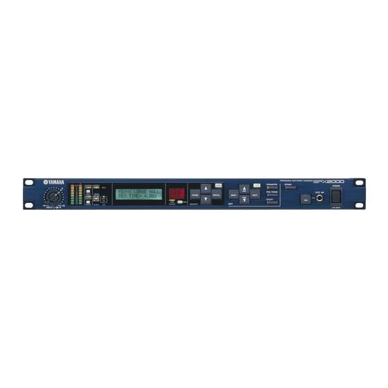
- Page 8 SPX2000 3 7 63 1515 0 (パネルレイアウト) PANEL LAYOUT (フロントパネル) Front Panel w e tu @0 @3 r yi @2 @1 q [INPUT L q [INPUT L R]コントロール R] control w Level meters w レベルメーター e [INPUT MODE] button/indicator e [INPUT MODE] ボタン/インジケーター...
- Page 9 SPX2000 3 7 63 1515 0 Rear Panel ( リアパネル) #1 #2 @7 Grounding screw @7 アース用ネジ @8 [AC IN] jack @8 [AC IN]端子 @9 [MIDI OUT/THRU] connector @9 [MIDI OUT/THRU]端子 #0 [MIDI IN] connector #0 [MIDI IN]端子 L 13942296513 #1 [TO HOST USB] connector #1 [TO HOST USB]端子...
- Page 10 SPX2000 3 7 63 1515 0 (ユニットレイアウト) CIRCUIT BOARD LAYOUT JKIN JKOUT POWER SUPPLY UNIT MAIN L 13942296513 LCD MODULE FOOTSW POWER u163 http://www.xiaoyu163.com...
- Page 11 SPX2000 3 7 63 1515 0 (分解手順) DISASSEMBLY PROCEDURE Rack Angle ラックアングル (所要時間 : 約1分) (Time required : About 1 min.) 1-1. [540A]のネジ3本を外し、 ラックアングルLを外しま 1-1. Remove the three (3) screws marked [540A]. The rack す。 (図1) angle L can then be removed. (Fig. 1) 1-2.
- Page 12 SPX2000 3 7 63 1515 0 Front Panel フロントパネル (所要時間 : 約3分) (Time required : About 3 min.) 3-1. ラックアングルL、 Rを外します。 (1項参照) 3-1. Remove the rack angle L and R. (See procedure 1) 3-2. トップカバーを外します。 (2項参照) 3-2. Remove the top cover. (See procedure 2) 3-3.
- Page 13 SPX2000 3 7 63 1515 0 MAIN Circuit Board MAINシート (所要時間 : 約5分) (Time required : About 5 min.) 5-1. ラックアングルL、 Rを外します。 (1項参照) 5-1. Remove the rack angle L and R. (See procedure 1) 5-2. トップカバーを外します。 (2項参照) 5-2. Remove the top cover. (See procedure 2) 5-3.
- Page 14 SPX2000 3 7 63 1515 0 VOL Circuit Board, FOOT SW Circuit VOLシート、 FOOT SWシート、 POWERシート Board, POWER Circuit Board (所要時間 : 各約4分) (Time required : About 4 minutes each.) 8-1. ラックアングルL、 Rを外します。 (1項参照) 8-1. Remove the rack angle L and R. (See procedure 1) 8-2.
- Page 15 SPX2000 3 7 63 1515 0 9-5. Remove the three (3) hooks from the LED guide. The 9-5. フック3箇所を外し、 LEDガイドからPN1シートを外し PN1 circuit board can then be removed. (Fig. 6) ます。 (図6) 9-6. Remove the two (2) hooks from the LED guide. The 9-6.
- Page 16 SPX2000 3 7 63 1515 0 (LSI 端子機能表) LSI PIN DESCRIPTION AK4393-VF-E2 (XW029A00) DAC (Digital to Analog Converter) ......20 CS5361-KS (X3447A00) ADC (Analog to Digital Converter) .
- Page 17 SPX2000 3 7 63 1515 0 HD6417709SF133 (X2081A00) CPU (SH3) MAIN: IC004 NAME FUNCTION NAME FUNCTION CKE/PTK5 CK enable / Port K Mode control RAS3L/PTJ0 RAS address bus / Port J Vcc(RTC) Power supply +1.8 V PTJ1 Port J...
- Page 18 SPX2000 YSS910-S (XV988A00) DSP6 (Digital Signal Processor) MAIN: IC303 3 7 63 1515 0 NAME FUNCTION NAME FUNCTION Power supply (3.3 V) Ground Ground DB13 System master clock input (60 MHz or 30 MHz) DB14 System master clock output (High or 30 MHz)
- Page 19 SPX2000 3 7 63 1515 0 CS8415A-CS (X2089A00) DIR (Digital Audio Interface Receiver) MAIN: IC401 NAME FUNCTION NAME FUNCTION CDOUT Data out (SPI) RXP4 Additional AES3/SPDIF receiver port Control port chip select (SPI) OSCLK Serial audio output bit clock...
- Page 20 SPX2000 3 7 63 1515 0 CS5361-KS (X3447A00) ADC (Analog to Digital Converter) MAIN: IC603 NAME FUNCTION NAME FUNCTION /RST Reset Mode selection M//S Master/slave mode LRCK Left right clock Test SCLK Serial clock AINL+ Differential left channel analog input...
- Page 21 SPX2000 3 7 63 1515 0 TC74VHC14FT (XV890A00) TC74VHC32FT (XY945A00) TC74VHC74FT (XV892A00) Hex Inverter Quad 2 Input OR Dual D-Type Flip-Flop MAIN: IC208 MAIN: IC012 MAIN: IC206 1CLR 2CLR INPUTS OUTPUTS TC74VHC244FT (XW234A00) TC74VHCT245AFT (XT744A00) 74LVX4245MTCX (X3097A00) Octal 3-State Bus Buffer...
- Page 22 SPX2000 3 7 63 1515 0 NJM2904V(TE1) (XR532A00) NJM4556AL (XP844A00) Dual Operational Amplifier Dual Operational Amplifier MAIN: IC002 MAIN: IC704, 754 +DC Voltage Output A Supply Inverting Output B Input A Non-Inverting Inverting Input A Input B Non-Inverting -DC Voltage Supply...
-
Page 23: Circuit Boards
SPX2000 3 7 63 1515 0 (シート基板図) CIRCUIT BOARDS PN3 Circuit Board BYPASS UNDO PARE PARAMETER BACK STORE RECALL FINE PARAM NEXT UTILITY to MAIN-CN503 Component side (部品側) L 13942296513 Pattern side (パターン側) PN1 Circuit Board PN2 Circuit Board Component side (部品側)... - Page 24 SPX2000 3 7 63 1515 0 INPUT OUTPUT MAIN Circuit Board +4dBu -10dBu +4dBu -10dBu (MONO) L 13942296513 u163 to VOL-CN601 to PN1-CN001 to LCD to POWER SUPPLY UNIT-CN51 2NAP-WB05300-1 http://www.xiaoyu163.com...
- Page 25 SPX2000 3 7 63 1515 0 AES/EBU WORD CLOCK MIDI OUT/THRU (TO HOST) L 13942296513 u163 Component side (部品側) to PN2-CN101 to PN3-CN201 to FOOTSW-CN701 2NAP-WB05300-1 http://www.xiaoyu163.com...
-
Page 26: Main Circuit Board
SPX2000 3 7 63 1515 0 MAIN Circuit Board L 13942296513 u163 2NAP-WB05300-2 http://www.xiaoyu163.com... - Page 27 SPX2000 3 7 63 1515 0 L 13942296513 u163 Pattern side (パターン側) 2NAP-WB05300-2 http://www.xiaoyu163.com...
- Page 28 SPX2000 3 7 63 1515 0 JKIN Circuit Board FOOTSW Circuit Board FOOT SW INPUT Component side (部品側) Component side (MONO) (部品側) Pattern side (パターン側) VOL Circuit Board Pattern side (パターン側) INPUT JKOUT Circuit Board Component side L 13942296513 (部品側)...
- Page 29 SPX2000 3 7 63 1515 0 Check Items INSPECTIONS 2-1. When ANALOG INPUT/OUTPUT WORD Preparations CLOCK is INT 96kHz 1-1. Conditions Condition: Use following conditions unless otherwise specified. Signals are inputted through ANALOG INPUT L, R • INPUT VOLUME: MAX (XLR) and output from ANALOG OUTPUT L, R •...
- Page 30 SPX2000 3 7 63 1515 0 [1] Distortion ratio (both L and R) b. WORD CLOCK INT 48kHz Condition: Set WORD CLOCK INT to 48kHz. Input frequency Output level Permissible range 1 kHz +23 dBu 0.02 % or below...
- Page 31 SPX2000 3 7 63 1515 0 Supplementary) b. WORD CLOCK EXT After this test, press the UTILITY key again and when Condition: Select the WORD CLOCK as follows. "INPUT SOURCE" appears on the LCD, press the DEC When checking WORD CLOCK IN: WORD CLOCK key.
- Page 32 SPX2000 3 7 63 1515 0 ■ 検査 1. 準備 2. 検査項目 1−1. 条件 2−1. ANALOG INPUT/OUTPUTのWORD CLOCK ◇ 特に指定しないときは以下の条件とします。 INT96kHz時検査 ・ INPUT VOLUME: MAX 条件 ANALOG INPUT L、 R(XLR)から入力し、 ANALOG ・ レベル切替SW: +4dBu側(入力、 出力共) OUTPUT L、 R(XLR)から出力します。 ・ アナログ出力の負荷は、 600Ωとします。...
- Page 33 SPX2000 3 7 63 1515 0 b. WORD CLOCK INT48kHz 2−2. ANALOG INPUT/OUTPUTのWORD CLOCK 条件 WORD CLOCK INTは48kHzにします。 INT48kHz時検査 条件 ANALOG INPUT L、 R(PHONE)から入力し、 ANALOG 歪率(AES/EBU OUT) OUTPUT L、 R(PHONE)から出力します。 入力周波数 出力レベル 許容範囲 1kHz −1dBFS 0. 02%以下 歪率 (L/R共) 入力周波数...
- Page 34 SPX2000 3 7 63 1515 0 b. WORD CLOCK EXT 2−6. WORD CLOCK IN, DIGITAL INのPLL動作範囲 条件 WORD CLOCKは以下を選択します。 条件 System Twoを使用します。 WORD CLOCK INの検査時 : WORD CLOCK ANALOG INPUT L、 R(XLR)から入力し、 ANALOG DIGITAL INの検査時 : AES/EBU OUTPUT L、 R(XLR)から出力します。...
- Page 35 (2) Clicking on this circle (1-1) will set USB=MIDI to THRU. If USB has become invalid by SPX2000 USB initialization, press the [OK] key to end the operation and start up the USB-MIDI driver once again. * Download the USB-MIDI driver from the YSISS Home Page.
- Page 36 SPX2000 3 7 63 1515 0 Starting Testing Turn on the power while pressing "UTILITY" and "NEXT" keys NEXT POWER UTILITY Entry screen SERVICE TEST SPX2000 V1.00 Displayed for a few seconds only. Operation Procedure Key on panel Function...
- Page 37 SPX2000 3 7 63 1515 0 List of check items Item Test name Outline of check item Judgment MCS(PLLP) Check the register of the gate array PLLP2 by reading/writing. Auto BATT Check the voltage of the back-up battery/ Auto DSP6,SIO Check the register of DSP6 by reading/writing and SIO connection.
- Page 38 SPX2000 3 7 63 1515 0 MIDI test Caution The character string "SCI2: TEST¥n" (¥n=0Ah) is sent Cancellation of this test is invalid while it is being from MIDI OUT to MIDI IN at 31.25 Kbps to check if executed.
- Page 39 SPX2000 3 7 63 1515 0 WORD CLOCK test "OK is displayed when the WORD CLOCK test ends The external oscillator OUT -> WORD CLOCK IN is with a satisfactory result and "NG" when it ends with an counted by PLLP2 for automatic check.
- Page 40 SPX2000 3 7 63 1515 0 10. PANEL LED test Whether the LEDs on the panel light up in the specified order or not is checked visually. Example of execution screen. PANEL LED LEDs light up in the lighting order as specified.
- Page 41 SPX2000 3 7 63 1515 0 PANEL SW test Press all the switches on the panel in the specified order, and their response is checked automatically. Example of execution screen PANEL SW The name of the switch to be pressed is displayed on the LCD.
- Page 42 SPX2000 3 7 63 1515 0 ■ テストプログラム 準備 ● 1) ケーブル類 XLR(AES/EBU): 1本 MIDI: 1本 USB: 1本 FC5またはOPEN JACK: 1個 2) 測定器 発振器 (出力インピーダンスは150Ωとします。 ) オシロスコープ (入力インピーダンスは100kΩ以上とします。 ) 3) パーソナルコンピューター (PC) : DOS/V機 本体のUSBコネクタとパソコンとをUSBケーブルで接続します。 パソコンに、 USB-MIDIドライバの設定をします。 USBドライバーは、 Windows9x系のものを用います。...
- Page 43 SPX2000 3 7 63 1515 0 起動方法 ● 「UTILITY」 + 「 NEXT」 を押しながら電源ONします。 NEXT POWER UTILITY エントリー画面 SERVICE TEST SPX2000 V1.00 数秒だけ表示 操作方法 ● パネル上のキー 機能 [MEMORY UP] テスト番号の順方向選択 [MEMORY DOWN] テスト番号の逆方向選択 [RECALL] 選択したテスト番号の実行開始 [UNDO] 実行中のテストの強制中止 L 13942296513 * 但しテスト項目によっては不可能なものもあります...
- Page 44 SPX2000 3 7 63 1515 0 検査項目一覧 ● 項目 検査名称 検査項目の概要 判定 MCS(PLLP) ゲートアレー PLLP2 のレジスタをW/Rし判定 自動 BATT バックアップ用電池の電圧を判定 自動 DSP6,SIO DSP6のレジスタをW/Rし判定、 SIO接続判定 自動 MIDI MIDI OUT-->INの送受信を判定 自動 USB MIDI USB回路の初期化、 外部PCでLoopBackし判定 自動 AES/EBU IN/OUT AES/EBU IN/OUT DIGITALをLoopBackし判定 半自...
- Page 45 SPX2000 3 7 63 1515 0 DSP6, SIO test USB MIDI test 内容 DSP6のRegisterをWrite/ReadしてDataBUS, Address 内容 USBを初期化後、 USB接続したパソコンのLoopBackで BUSの良否を判定します。 自動判定をします。 DSP6 のDRAMにRegister経由でWrite/Readして比較判 定します。 準備 本体のUSBコネクタとパソコンとを汎用のUSBケー DSP6のOUT METER SIO結線を、 信号の送受信で判定 ブルで接続します。 します。 パソコンに、 USB-MIDI ドライバの設定をします。 (Thru On) 実行画面例 実行画面例 DSP6 bit23,3,0 USB MID テストが開始されると、...
- Page 46 SPX2000 3 7 63 1515 0 注意事項 “WC disconnect!” と表示したら、 IN->OUT 接続されてい 1) DIR Lock flagは、 Gate Array にてReadします(SIO送受信開 るWORD CLOCK OUT信号を切り離します。 始後約100mS待って判定)。 準備が終わったら、 [NEXT] スイッチを押します。 2) DIT,DIR,CDIN,CDOUTのWrite/ReadでRUN bit(Reg4の ここでキャンセルをする場合、 [UNDO] か [BACK] スイッ 0x40)を確認します。 チのどちらかを押します。 WORD CLOCK test WORD CLOCK テストが正常終了すれば、...
- Page 47 SPX2000 3 7 63 1515 0 PANEL LED test 内容 パネル上のLEDが規定の順序で点灯するかを目視で 確認します。 実行画面例 PANEL LED 点灯順序に従い、 LED を点灯します。 最後に、 全ての LED を点灯します。 正常に点灯する場合、 OKとして、 [NEXT]を押します。 NGの場合、 [BACK]を押します。 PANEL LED テストが正常終了すれば、 “ OK” が表示され ます。 もし、 異常終了すれば、 “ NG” が表示されます。...
- Page 48 SPX2000 3 7 63 1515 0 PANEL SW test 内容 パネル上の全てのスイッチを規定順序通り押して反 応するか検査します(自動判定)。 実行画面例 PANEL SW LCDに、 押すべきスイッチ名称を表示します。 押されたことが確認できたら、 次の押すべきスイッチ名称 を表示します。 最後に、 FOOT SWと表示されたら、 OPEN JACKをFOOT SW端子に挿入します。 期待するスイッチが押されるまで無限ループです。 テストを強制終了したい場合は、 [BACK]を押し、 テスト NGとします。 PANEL SW テストが正常終了すれば、 “ OK” が表示され ます。 もし、 異常終了すれば、 “ NG” が表示される。...
- Page 49 (YSISS URL >>http://plaza.yamaha.co.jp/ysiss/exindex.nsf) てください。 (URL >>http://plaza.yamaha.co.jp/ysiss/index.nsf) Confirming Program Version プログラムのバージョンの確認方法 While pressing the [UTILITY] key, turn on the main power to the SPX2000. Then, the version of the main UTILITYキーを押しながら SPX2000本体の電源を入 program appears on the LCD screen. れるとLCD画面に本体プログラムのバージョンが表 示されます。 POWER...
- Page 50 L 13942296513 with the transmitted data. ません。 INITIALIZING THE SPX2000 (初期化) Here’s how to return the SPX2000 to its factory-set condi-tion. SPX2000 を工場出荷時の状態に戻します。 以下の操作をすると、 USER バンクのエフェクトがすべて消 The following procedure will erase all effects in the USER 去されます。 初期化の前に必要に応じて、 「 BULK OUT(ALL)」...
- Page 51 There is no effect to recall. Please re-select an effect to recall. Sync Error! The clock of the received digital input signal differs from the SPX2000’s operating clock. This BANK is Protected! You selected the PRESET bank or CLASSIC bank as the effect store-destination.
- Page 52 受信しているデジタル入力信号とSPX2000の動作しているCLOCKが違います。 This BANK is Protected! エフェクトのストア先がPRESETバンクまたはCLASSICバンクになっています。 PRESETバンクやCLASSICバンクは読み出し専用のためエフェクトのストアやエフェクト名の 変更、 プロテクトの設定、 ディスプレイ背景色の変更ができません。 どれかボタンを押してエラー を解除したあと、 USERバンクからストア先を選択してください。 This Program is Protected! エフェクトのストア先にプロテクトがかかっています。 どれかボタンを押してエラーを解除したあと、 必要に応じてプロテクトを解除してください。 USB Rx Buffer Full! USBの受信バッファーが一杯になりました。 どれかボタンを押してエラーを解除したあと、 もう一度MIDIデータを送り直してみてください。 エラーが再発する場合にはMIDIデータの送信間隔をあけるなどして、 一度に大量のMIDIデータ が送り込まれないようにしてください。 WRONG WORD CLOCK! 外部からのワードクロック信号が途切れているか、 SPX2000で同期可能な周波数ではありませ ん。 ワードクロックを供給する機器との接続やワードクロックの設定に問題がないかご確認く ださい。 u163 http://www.xiaoyu163.com...
- Page 53 SPX2000 3 7 63 1515 0 MIDI IMPLEMENTATION CHART YAMAHA [PROFESSIONAL MULTI-EFFECT PROCESSOR] Date: 12 MAY 2003 MIDI Implementation Chart Model: SPX2000 Version: 1.0 Function... Transmitted Recognized Remarks Basic Default 1–16 Memorized Channel Changed 1–16 Default OMNI OFF/OMNI ON...
-
Page 54: Midi Data Format
2.3 CONTROL CHANGE (Bn) Type (HEX) rx/tx function When the SPX2000 receives this message, it will operate in one of two Edit buffer 1 (01) rx/tx ways. The operation will depend on the content of the first two bytes of... -
Page 55: Http://Www.xiaoyu163.Com
No-1) FORMAT No. 01111110 Universal bulk dump Bulk Dump messages are used to bulk dump SPX2000 data to a con- Bulk Dump messages are used to bulk dump SPX2000 data to a con- 01001100 ’L’ nected MIDI device, or to receive data from a connected MIDI device to... - Page 56 00000010 256:EDIT BUFFER L 13942296513 00000000 No.256 = Current For reception by the SPX2000, only USER 1-99 or EDIT BUFFER are 11110111 End of exclusive valid. (120-220, 256) 2.8.2 Program change table Bulk Dump request For- 2.8.1.4 Effect Program Bulk Dump request Format The second and third byte of DATA NAME specify the program number.
- Page 57 'ee' will be expanded to two bytes) the change. At this time, the device number will be the MIDI channel of 0ppppppp Parameter no. the SPX2000. If the MIDI channel is OMNI, the device number will be 1. 0ccccccc Channel no. 11110111 End of exclusive •...
- Page 58 DATA 00000000 change. At this time, the device number will be the MIDI channel of the 0eeeeeee Effect number (0) SPX2000. If the MIDI channel is OMNI, the device number will be 1. 11110111 End of exclusive • Format function...
- Page 59 The device number used when transmitting meter data will be the MIDI channel of the SPX2000. If the MIDI channel is OMNI, the device num- L 13942296513 ber will be 1.
-
Page 60: Http://Www.xiaoyu163.Com
http://www.xiaoyu163.com 3 7 63 1515 0 PARTS LIST CONTENTS (目次) OVERALL ASSEMBLY (総組立) ..........2 ELECTRICAL PARTS (電気部品) ........5 – 15 L 13942296513 Notes : DESTINATION ABBREVIATIONS A : Australian model M : South African model B : British model O : Chinese model C : Canadian model Q : South-east Asia model... - Page 61 SPX2000 3 7 63 1515 0 OVERALL ASSEMBLY (総組立) 550 560 110a L 13942296513 110b 110f Rubber cap (ラバーキャップ) 110d WC049600 See page 5. u163 110h 110e 110c 110g Rubber cap (ラバーキャップ) WC049600 PN3 circuit board See page 5.
- Page 62 SPX2000 3 7 63 1515 0 • Pic. 1 MAIN-POWER SUPPLY wiring • Pic. 2 AC INLET-POWER wiring 280 290 POWER AC INLET POWER SUPPLY UNIT MAIN POWER SUPPLY UNIT • AC inlet assembly L 13942296513 140b 140d 140a...
- Page 63 SPX2000 3 7 63 1515 0 PART NO. DESCRIPTION REMARKS 部 品 名 REF NO. RANK 総 組 立 OVERALL ASSEMBLY SPX2000 (WB42170) ボトムシャーシAss’y WB424200 Bottom Chassis EP630210 Bind Head Tapping Screw-S 3.0X6 MFZN2BL + バ イ ン ド S タ イ ト...
- Page 64 SPX2000 3 7 63 1515 0 ELECTRICAL PARTS (電気部品) PART NO. DESCRIPTION 部 品 名 REMARKS REF NO. RANK ELECTRICAL PARTS 電 気 部 品 SPX2000 AAX51290 Circuit Board FOOTSW F O O T S W シ ー ト...
- Page 65 SPX2000 3 7 63 1515 0 PART NO. DESCRIPTION 部 品 名 REMARKS REF NO. RANK * LD019 WC153200 LED (chip) Yellow TLYV1020 J,K チ ッ プ L E D キ CLIP L -12 LD020 WA587900 LED (chip) Red TLSU1020 チ...
- Page 66 SPX2000 3 7 63 1515 0 PART NO. DESCRIPTION 部 品 名 REMARKS REF NO. RANK BT001 VN103600 Battery Holder CR2032 バ ッ テ リ ー ホ ル ダ ー C001 US145100 Ceramic Capacitor-F (chip) 0.1000 25V Z チ ッ プ セ ラ ( F )...
- Page 67 SPX2000 3 7 63 1515 0 PART NO. DESCRIPTION 部 品 名 REMARKS REF NO. RANK C428 UF037100 Electrolytic Cap. (chip) 10 16V チ ッ プ ケ ミ コ ン C429 US145100 Ceramic Capacitor-F (chip) 0.1000 25V Z チ ッ プ セ ラ ( F )...
- Page 68 SPX2000 3 7 63 1515 0 PART NO. DESCRIPTION 部 品 名 REMARKS REF NO. RANK * C704 WC153700 Electrolytic Cap. 22.00 50.0V ケ ミ コ ン S M E C705 US145100 Ceramic Capacitor-F (chip) 0.1000 25V Z チ...
-
Page 69: Table Of Contents
SPX2000 3 7 63 1515 0 PART NO. DESCRIPTION 部 品 名 REMARKS REF NO. RANK D803 V 8 4 0 9 2 0 0 Diode RB160L-60 ダ イ オ ー ド D804 VS597600 Diode RB160L-40 TE25 ダ イ... - Page 70 SPX2000 3 7 63 1515 0 PART NO. DESCRIPTION 部 品 名 REMARKS REF NO. RANK IC652 XF291A00 UPC4570G2 I C OP AMP IC701 XW029A00 AK4393-VF-E2 I C IC702 NJM78L05UA I C REGULATOR +5V XJ598A00 I C IC703 XF291A00...
- Page 71 SPX2000 3 7 63 1515 0 PART NO. DESCRIPTION 部 品 名 REMARKS REF NO. RANK R209 RD355150 Carbon Resistor (chip) 150.0 63M J チ ッ プ 抵 抗 R210 RD356150 Carbon Resistor (chip) 1.5K 63M J チ ッ...
- Page 72 SPX2000 3 7 63 1515 0 PART NO. DESCRIPTION 部 品 名 REMARKS REF NO. RANK R608 VC328500 Metal Film Resistor 7.5K 1/4 F 金 属 被 膜 抵 抗 * R609 VC329900 Metal Film Resistor 30.0K 1/4 F 金...
- Page 73 SPX2000 3 7 63 1515 0 PART NO. DESCRIPTION 部 品 名 REMARKS REF NO. RANK R714 VC326800 Metal Film Resistor 1.5K 1/4 F 金 属 被 膜 抵 抗 R715 VC328400 Metal Film Resistor 6.8K 1/4 F 金...
- Page 74 SPX2000 3 7 63 1515 0 PART NO. DESCRIPTION 部 品 名 REMARKS REF NO. RANK RA201 RE047100 Resistor Array 10KX4 抵 抗 ア レ イ RA401 RE047470 Resistor Array 47KX4 抵 抗 ア レ イ RA402 RE047470 Resistor Array 47KX4 抵...
- Page 75 http://www.xiaoyu163.com 3 7 63 1515 0 CIRCUIT DIAGRAM CONTENTS (目次) BLOCK DIAGRAM (ブロックダイアグラム) ......3 OVERALL CONNECTOR CIRCUIT DIAGRAM (総コネクタ接続回路図) ..............4 L 13942296513 OVERALL CIRCUIT DIAGRAM (総回路図) MAIN (001-009) ............5 – 13 PN1-3, POWER, JKIN, JKOUT, VOL, FOOTSW ....14 Notation for Circuit Diagrams (回路図表記上の注意)...
-
Page 76: Q Q I I
3 7 6 3 1 5 1 5 0 SPX2000 BLOCK DIAGRAM INPUT MAIN CN601 CN602 JK601 +15A (MONO) +15A JKIN IC601 INPUT IC601, 602 CN601 VR601 (MONO) 2ch/line M64FS/MWC/ANA256FS -15A -15A +4dBu /RESADA CS5361 JK401 +15A SW601 IC651, 652... - Page 77 3 7 6 3 1 5 1 5 0 SPX2000 OVERALL CONNECTOR CIRCUIT DIAGRAM Metal fitting + nut (金具 + ナット) P.C.B. installation screw Metal fitting + nut (基板取付ネジ) (金具 + ナット) LCD MODULE FOOTSW CN201 CN101 CN001 CN601...
-
Page 78: Regulator +1.8V
3 7 6 3 1 5 1 5 0 SPX2000 OVERALL CIRCUIT DIAGRAM 001 (MAIN 1/9) RB500V-40 (V2376600) µ PC2918T-E1(X2157A00) DIODE REGULATOR +1.8V 1: INPUT to FOOTSW-CN701 2: GND 1: ANODE 3: OUTPUT 2: CATHODE 4: GND REGULATOR +1.8V... -
Page 79: Transceiver
3 7 6 3 1 5 1 5 0 SPX2000 OVERALL CIRCUIT DIAGRAM 002 (MAIN 2/9) TRANSCEIVER LEVEL CHANGE 1 3 9 4 2 2 9 6 5 1 3 w w w u 1 6 3 XX : not installed(未実装部品)... -
Page 80: Transceiver
3 7 6 3 1 5 1 5 0 SPX2000 OVERALL CIRCUIT DIAGRAM 003 (MAIN 3/9) TRANSCEIVER INVERTER INVERTER INVERTER NAND INVERTER RESET 1 3 9 4 2 2 9 6 5 1 3 NAND DIR2 PLLP2 (Clock Generator) XX : not installed(未実装部品)... -
Page 81: Dram 4M
3 7 6 3 1 5 1 5 0 SPX2000 OVERALL CIRCUIT DIAGRAM 004 (MAIN 4/9) DRAM DSP6 1 3 9 4 2 2 9 6 5 1 3 not installed w w w u 1 6 3 OVERALL CIRCUIT DIAGRAM 004 (MAIN 4/9) 28CC1-8828883-4 1 http://www.xiaoyu163.com... - Page 82 3 7 6 3 1 5 1 5 0 SPX2000 OVERALL CIRCUIT DIAGRAM 005 (MAIN 5/9) TO HOST 1SS372 (V9424900) DIODE ARRAY USB CPU BUFFER 1: ANODE1 2: CATHODE2 3: CATHODE1, ANODE2 Photo Coupler 1 3 9 4 2 2 9 6 5 1 3...
- Page 83 3 7 6 3 1 5 1 5 0 SPX2000 OVERALL CIRCUIT DIAGRAM 006 (MAIN 6/9) RESET INVERTER Transistor Array to PN1-CN001 1 3 9 4 2 2 9 6 5 1 3 to PN2-CN101 to PN3-CN201 Transistor Array...
- Page 84 3 7 6 3 1 5 1 5 0 SPX2000 OVERALL CIRCUIT DIAGRAM 007 (MAIN 7/9) OP AMP (MONO) OP AMP OP AMP INPUT TRANSCEIVER INPUT to JKIN-CN401 INVERTER to VOL-CN601 OP AMP OP AMP OP AMP 1 3 9 4 2 2 9 6 5 1 3 w w w XX : not installed(未実装部品)...
- Page 85 3 7 6 3 1 5 1 5 0 SPX2000 OVERALL CIRCUIT DIAGRAM 008 (MAIN 8/9) OP AMP OP AMP OP AMP MUTE OUTPUT to JKOUT-CN501 OUTPUT OP AMP OP AMP MUTE REGULATOR OP AMP 1 3 9 4 2 2 9 6 5 1 3...
- Page 86 3 7 6 3 1 5 1 5 0 SPX2000 OVERALL CIRCUIT DIAGRAM 009 (MAIN 9/9) REGULATOR +15V REGULATOR REGULATOR -15V 1 3 9 4 2 2 9 6 5 1 3 RB160L-60 (V8409200) RB160L-40 (VS597600) HZK3CTR3.3V (V9544100) RLZ11B11.0V (VK040100)
- Page 87 3 7 6 3 1 5 1 5 0 SPX2000 OVERALL CIRCUIT DIAGRAM (PN1-3, POWER, JKIN, JKOUT, VOL, FOOTSW) POWER to POWER SUPPLY UNIT-CN1 to MAIN-CN501 to AC INLET JKIN (MONO) INPUT to MAIN-CN601 CLASSIC to MAIN-CN502 JKOUT 1 3 9 4 2 2 9 6 5 1 3...