Table of Contents
Advertisement
SERVICE MANUAL
COMPACT COMPONENT SYSTEM
SOUND
VOCAL
MODE
MASKING
ECHO
SLEEP
FM MODE
V.INTRO
HIGHLIGHT
SUBTITLE
STILL
A/B
TAPE
REC
START/STOP
ACTIVE
BASS EX.
ON SCREEN
PREV
NEXT
KEY CONTROL
FADE
MUTING
RM—SMXJ570V REMOTE CONTROL
Each difference point
Model
CD/DECK/RECEIVER
MX-J570V
CA-MXJ570V
MX-J680V
CA-MXJ680V
Contents
Safety precautions
Important for laser products
Preventing static electricity
Precautions at disassembling
and parts replacement
Disassembly method
Adjustment method
MX-J570V
MX-J680V
SUPER VIDEO
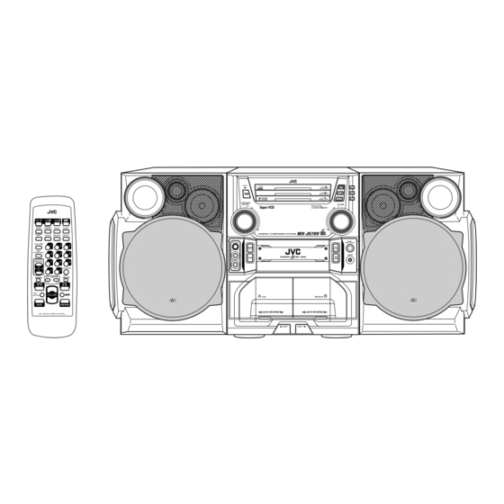
This illustration is MX-J570V
SPEAKER
Tray fitting
SP-MXJ570V
Silver
SP-MXJ680V
1-2
1-3
1-4
1-5
1-6
1-29
COPYRIGHT
2000 VICTOR COMPANY OF JAPAN, LTD.
US
UX
Color
Panel
Light blue
Silver & Blue
Champagne-gold
Diagnosis which uses
extension wire method
Flow of functional operation
until TOC read
Maintenance of laser pickup
Replacement of laser pickup
Description of major ICs
MX-J570V
MX-J680V
Area Suffix
Singapore
Saudi Arabia
COMPACT
DIGITAL VIDEO
COMPACT
SUPER VIDEO
COMPACT
DIGITAL AUDIO
Net
Front
Silver
Champagne-gold
Gray
1-33
1-34
1-35
1-35
1-36
No.20853
Jul. 2000
Advertisement
Table of Contents

Related Manuals for JVC MX-J570V


Summary of Contents for JVC MX-J570V
- Page 1 START/STOP ACTIVE BASS EX. ON SCREEN COMPACT PREV NEXT KEY CONTROL FADE MUTING SUPER VIDEO RM—SMXJ570V REMOTE CONTROL COMPACT This illustration is MX-J570V DIGITAL AUDIO Each difference point Color Model CD/DECK/RECEIVER SPEAKER Front Tray fitting Panel MX-J570V CA-MXJ570V SP-MXJ570V Light blue Silver &...
-
Page 2: Safety Precautions
MX-J570V/MX-J680V Safety Precautions 1. This design of this product contains special hardware and many circuits and components specially for safety purposes. For continued protection, no changes should be made to the original design unless authorized in writing by the manufacturer. -
Page 3: Important For Laser Products
MX-J570V/MX-J680V Important for laser products 5.CAUTION : If safety switches malfunction, the laser is able 1.CLASS 1 LASER PRODUCT to function. 2.DANGER : Invisible laser radiation when open and inter 6.CAUTION : Use of controls, adjustments or performance of lock failed or defeated. Avoid direct exposure to beam. -
Page 4: Preventing Static Electricity
MX-J570V/MX-J680V Preventing static electricity 1. Grounding to prevent damage by static electricity Electrostatic discharge (ESD), which occurs when static electricity stored in the body, fabric, etc. is discharged, can destroy the laser diode in the traverse unit (optical pickup). Take care to prevent this when performing repairs. - Page 5 MX-J570V/MX-J680V Precautions at disassembling and parts replacement This model is charged with electricity on the power board even if the power cord is unplugged. Therefore, always discharge electricity in accordance with the steps given below before starting disassembling of the unit and/or replacement of parts.
- Page 6 MX-J570V/MX-J680V Disassembly method Metal cover <Main body> Removing the metal cover (See Fig.1 to 3) Remove the six screws A attaching the metal cover on the back of the body. Remove the two screws B attaching the metal cover on both sides of the body.
- Page 7 MX-J570V/MX-J680V Removing the CD changer mechanism Video CD board CD changer assembly (See Fig.4 to 6) mechanism assembly Prior to performing the following procedure, remove Rear panel Front panel assembly the metal cover. For the card wire connecting the CD changer mechanism board and the main board, disconnect it from connector CN868 on the main board.
- Page 8 MX-J570V/MX-J680V Removing the front panel assembly (See Fig.8 to 10) Prior to performing the following procedure, remove Front panel assembly the metal cover and the CD changer mechanism assembly. Disconnect the card wire from connector CN865 on the main board and pull out the earth wire on the main board.
- Page 9 MX-J570V/MX-J680V <Front panel assembly> Removing the Microphone terminal board assembly (See Fig.11 and 12) Prior to performing the following procedure, remove the metal cover, CD changer mechanism assembly and the front panel assembly. Pull out the MIC volume knob from the front side.
- Page 10 MX-J570V/MX-J680V Main board Removing the main board CN867 (See Fig.14 and 15) CN879 Prior to performing the following procedure, remove the front panel assembly, the microphone terminal board and the rolling panel assembly. Disconnect the harness from connector CN867 on the main board.
- Page 11 MX-J570V/MX-J680V Removing the boards in the front panel assembly (See Fig.17 and 18) Prior to performing the following procedure, remove the front panel assembly, the microphone terminal board assembly and the rolling panel assembly. Function Function Function board1 (See Fig.17)
- Page 12 MX-J570V/MX-J680V Power switch board (See Fig.19) Remote control port board Eject swith Power swith board Remove the two screws T attaching the power board switch board. Unsolder FW951 on the power switch board and disconnect the harness extending to the FW850 bass-level regulator board.
- Page 13 MX-J570V/MX-J680V <Rear panel assembly> Tuner board Rear panel Joint board Removing the tuner board CN871 (See Fig.21 and 22) Plastic rivets Prior to performing the following procedure, remove the metal cover and CD changer mechanism CN870 assembly. Remove the two plastic rivets attaching the joint CN612 board, and remove the joint board.
- Page 14 MX-J570V/MX-J680V Removing the rear cover / rear panel Rear panel (See Fig.23 to 26) Prior to performing the following procedure, remove the metal cover and the CD changer mechanism assembly. There is no need to remove the front panel assembly.
- Page 15 MX-J570V/MX-J680V Removing the pre-amplifier board / heat sink (See Fig.27 to 29) Relay board Prior to performing the following procedure, remove CN901 Pre-amplifier board the metal cover, the CD changer mechanism CN713 assembly and the rear cover / rear panel.
- Page 16 MX-J570V/MX-J680V Removing the power & main amplifier board (See Fig.30 and 31) Plastic rivet Plastic rivet Prior to performing the following procedure, remove the metal cover, the CD changer mechanism assembly, the front panel assembly, the rear cover / rear panel, the tuner board, the input / output board and pre-amplifier board.
- Page 17 MX-J570V/MX-J680V <Rolling panel assembly> Multi-control assembly Removing the multi-control assembly (See Fig.32 to 34) Prior to performing the following procedure, remove the metal cover, CD changer mechanism assembly, the front panel assembly, the microphone terminal board assembly, the rolling panel assembly and the main board.
- Page 18 MX-J570V/MX-J680V Removing the drive motor assembly Rolling panel assembly (See Fig.38 to 40) Prior to performing the following procedure, remove the metal cover, CD changer mechanism assembly, the front panel assembly, the microphone terminal board assembly, the rolling panel assembly and the main board.
- Page 19 MX-J570V/MX-J680V Removing the super VCD control board (See Fig.41) Prior to performing the following procedure, remove the metal cover and the CD changer mechanism CD changer assembly. mechanism assembly Disconnect the card wire from connector CN101 and CN102 CN101 CN102 on the super VCD control board.
- Page 20 MX-J570V/MX-J680V Removing the CD Servo control board (See Fig.1) 1.Remove the metal cover. 2.Remove the CD changer mechanism assembly. 3.From bottom side the CD changer mechanism assembly, remove the two screws A retaining the CD servo control CN854 board. 4.Absorb the four soldered positions "a" of the right and left motors with a soldering absorber.
- Page 21 MX-J570V/MX-J680V Stopper Check whether the lifter unit stopper has been caught into the hole at the section "e" of CD tray assembly as shown in Fig.5. Make sure that the driver unit elevator is positioned as shown in Fig.6 from to the second or fifth hole on the left side face of the CD changer mechanism assembly.
- Page 22 MX-J570V/MX-J680V Cams R1, R2 assembly Removing the CD loading mechanism assembly(See Fig.10) While turning the cams R1 and R2 assembly in the arrow direction "h" ,align the shaft "i" of the CD loading mechanism assembly to the position shown in Fig.10.
- Page 23 MX-J570V/MX-J680V Removing the cam unit (See Fig.14 ~17 ) Remove the CD loading mechanism assembly. While turning the cam gear "q", align the pawl "r" position of the drive unit to the notch position(Fig.16) on the cam gear "q". Pull out the drive unit and cylinder gear(See Fig.17).
- Page 24 MX-J570V/MX-J680V Removing the actuator motor and belt Gear bracket (See Fig.18~21) Remove the two screws K retaining the gear bracket (See Fig.19). While pressing the pawl "t" fixing the gear bracket in the arrow direction, remove the gear bracket Pulley gear (See Fig.19).
- Page 25 MX-J570V/MX-J680V Slit washer Removing the cams R1/R2 assembly and cam gear q(See Fig.22) Cam R2 Slit washer Remove the slit washer fixing the cams R1 and R2 assembly. Cam gear q By removing the two pawls "w" fixing the cam R1, separate R2 from R1.
-
Page 26: Cassette Mechanism Section
MX-J570V/MX-J680V < Cassette mechanism section > Cassette mechanism Removing the playback,recording and eraser heads (See Fig.1~3) 1. While shifting the trigger arms seen on the right side of the head mount in the arrow direction,turn Flywheel R the flywheel R in counterclockwise direction until the head mount has gone out with a click (See Fig. - Page 27 MX-J570V/MX-J680V Removing the head amp.and mechanism control P.C.board (See Fig. 4) 1.Remove the cassette mechanism assembly. Head amplifier & 2.After turning over the cassette mechanism mechanism control board assembly,remove the five screws "A" retaining the head amp. and mechanism control P.C.
- Page 28 MX-J570V/MX-J680V Removing the capstan motor (See Fig. 8) Capstan motor From the joint bracket, remove the two screws "C" retaining the capstan motor. Joint bracket Removing the flywheel (See Fig. 9,10) 1.Remove the head amp. and mechanism control P.C.Board. 2.Remove the capstan motor assembly.
-
Page 29: Adjustment Method
MX-J570V/MX-J680V Adjustment method Measurement instruments required for a djustment Radio input signal 1. Low frequency oscillator, AM modulation frequency : 400Hz This oscillator should have a capacity to output 0dBs Modulation factor : 30% to 600ohm at an oscillation frequency of 50Hz-20kHz. - Page 30 MX-J570V/MX-J680V Arrangement of adjusting positions Cassette mechanism section (Mechanism A section) Cassette mechanism section (Back side) Head azimuth Head azimuth adjusting screw adjusting screw (Reverse side) (Forward side) Head azimuth Head azimuth Playback,recording and eraser adjusting screw adjusting screw Playback...
- Page 31 MX-J570V/MX-J680V Tape recorder section Adjusting Items Measurement Standard Measurement method positions conditions values Confirmation Adjust the head Test tape Maximum 1.Playback the test tape TMT7036(10kHz). of head angle azimuth screw :TMT7036(10kHz) output 2.With the playback mechanism or recording only when the...
- Page 32 MX-J570V/MX-J680V Electrical performance Adjusting Items Measurement Standard Measurement method positions conditions values Adjustment of AC-225 *Mode : Forward or 1.With the recording and playback mechanism, recording bias :4.20 A reverse mode load the test tapes(AC-514 to TYP and AC-225 to...
- Page 33 MX-J570V/MX-J680V Diagnosis which uses extension wire method System control P.C.board 1.Remove the metal cover and CD changer mechanism. 2.Remove the front panel assembly. 3.One screw A is removed, and relay board is removed. 4.As shown in fig.1, place the front panel assembly after opening it outward using the right side of the front panel as an axis.
-
Page 34: Flow Of Functional Operation Until Toc Read
MX-J570V/MX-J680V Flow of functional operation until TOC read Check Point Slider turns REST Play Key Power ON Confirm that the voltage at the pin5 SW ON. of CN801 is "H"\"L"\"H". Automatic tuning of TE offset Check that the voltage at the... - Page 35 MX-J570V/MX-J680V Maintenance of laser pickup Replacement of laser pickup (1) Cleaning the pick up lens Before you replace the pick up, please try to Turn off the power switch and,disconnect the clean the lens with a alcohol soaked cotton power cord from the ac outlet.
-
Page 36: Description Of Major Ics
MX-J570V/MX-J680V Description of major ICs AN8806SB-W (IC601) : RF&Servo AMP 1.Pin layout PDAC PDBD LDON PDER PDFR TBAL RF OUT FBAL RF IN C.AGC EF OUT C.ENV TE OUT C.EA CROSS CS BDO TE BPF VDET CS BRT LD OFF... - Page 37 MX-J570V/MX-J680V 3. Pin function Pin No. Symbol Description APC amp input terminal APC amp output terminal LD ON APC ON/OFF control terminal Connect to ground Power supply Inverse input pin for RF amp RFamp output RF OUT RF IN RF input Connecting pin of AGC loop filter C.AGC...
- Page 38 MX-J570V/MX-J680V BA15218 (IC526) : OP AMP. OUT1 -IN1 OUT2 +IN1 -IN2 +IN2 BA3126N (IC301) : SWITCH 1. Terminal layout and Block diagram GP1U281X (IC915) : Receiver for remote controller – Limiter Integrator Comparator Amp. Demodulator B.P.F Vout 1-38...
- Page 39 MX-J570V/MX-J680V BA3835S (IC812) : SPI B.P.F. 1.Block Diagrams BIASC BIAS AOUT VREFC VREF REFERENCE RREF TEST CURRENT N.C. N.C. PEAK 105Hz HOLD N.C. N.C. PEAK 340Hz HOLD PEAK 1kHz DIFOUT HOLD PEAK 3.4kHz HOLD PEAK 10.5kHz HOLD 2.Pin Function Symbol Function Decoupling condenser connection terminal.
- Page 40 MX-J570V/MX-J680V BA3837(IC466):MIC Mixer 1.Block diagram ROUT LOGIC LOUT BIAS 2.Pin function Symbol Description Pin No. Power supply Microphone mixing input MIC IN Channel L output LOUT Non connect Non connect Channel L input Signal bias BIAS Connect to GND Channel R input...
- Page 41 MX-J570V/MX-J680V BU1427K (IC152) : Digital RGB-TV encoder 1. Terminal layout 2. Pin function NAME FUNCTION NAME FUNCTION BOSD OSD BLUE DATA INPUT SLABEB SELECT MASTER/SLAVE Y0/YUV0 YUV DATA ADDH +0.5/-0.5 LINE at NON-INTER Y1/YUV1 YUV DATA VREF-C DAC BIAS Y2/YUV2...
- Page 42 MX-J570V/MX-J680V BU9253AS(IC902) : LPF&ECHO MIX. 1.Pin layout & block diagram MUTE ECHO VR BIAS ADINT IN DAINT IN ADINT OUT DAINT OUT ADLPF OUT DALPF IN ADLPF IN DALPF OUT MIX IN MIX OUT 2.Pin function Descriptions Pin No. Symbol...
- Page 43 MX-J570V/MX-J680V HD74HCT244FP-XE (IC181) : Buffer 2. Block diagram 1. Terminal layout (Top View) 1-43...
- Page 44 MX-J570V/MX-J680V KM416S1020CTG10 (IC104) : 16Mb SDRAM 1. Terminal layout DQ15 DQ14 DQ13 DQ12 DQ11 DQ10 LDQM N.C/RFU UDQM A10/AP 2. Pin function Pin name Function System clock Chip select Clock enable Address Bank select address Row address strobe Column address Strobe...
- Page 45 MX-J570V/MX-J680V LA1838(IC1): FM AM IF AMP&detector, FM MPX decoder 1. Block Diagram DECODER RF.AMP ANIT-BIRDIE MUTE BUFF STEREO P-DET AM IF PILOT 384KHz COMP S-METER AM/FM S-CLRVE S-METER IF-BUFF TUNING STEREO DRIVE DRIVE FM IF 2. Pin Function Symbol Function...
- Page 46 MX-J570V/MX-J680V LA6541-X(IC801) : Servo Driver 1. Pin Layout & Block Diagram Vref Vin4 Vin3 Level B T L B T L Level RESET shift driver driver shift Level B T L B T L Level Regulator shift driver driver shift...
- Page 47 MX-J570V/MX-J680V LB1641 (IC853) : DC Motor Driver 1. Pin Layout GND OUT1 P1 IN2 VCC1 VCC2 P2 OUT2 2. Pin Functions Input Output Mode OUT1 OUT2 Brake CLOCKWISE COUNTER-CLOCKWISE Brake NJM4580L (IC901) : Mic Amplifier 1. A OUTPUT 2. A-INPUT 3.
- Page 48 MX-J570V/MX-J680V NJM4580E-W(IC652) : OP amp 1. Terminal layout A OUT B OUT 2. Block diagram INPUT OUTPUT 1-48...
- Page 49 MX-J570V/MX-J680V MN35511(IC651) : Digital servo & processor 1.Pin layout 2.Block diagram VCOF2 AVDD2 DEMP/TEST2 OUT2D 8tims OUT2C Over VCO2 Sampling Method LRCKI BCKI OUT1D Digital SDATAI Filter OUT1C IOSEL AVSS2 BLKCK CLDCK FLAG SBCK SBCK2 IP FLAG SUBC DEMPO Digital...
- Page 50 MX-J570V/MX-J680V 3. Pin function symbol I/O Description symbol I/O Description Non connect BCLK Bit clock output for SRDATA Identification signal output of Lch and Rch LRCK PLAY Non connect SRDATA Non connect Serial data output WVEL DVDD1 Power supply (Digital)
- Page 51 MX-J570V/MX-J680V TC74VHC00FT-X(IC106) : Wright timing control 1.Terminal layout / Block diagram TC74VHC74FT-X (IC107) : Flip-Flop 1CLR 1 2CLR (TOP VIEW) 1-51...
- Page 52 MX-J570V/MX-J680V TDA7439 (IC436) : Conrtol volume 1.Pin layout DIG GND TREBLE(R) AGND TREBLE(L) ROUT MIN(L) LOUT MOUT(L) R-IN4 BOUT(L) R-IN3 BIN(L) R-IN2 BOUT(R) R-IN1 BIN(R) L-IN1 MOUT(R) L-IN2 MIN(R) L-IN3 L-IN4 MUXOUTR MUXOUTL TDA7439 2.Block diagram L-IN1 SPEAKER AGND TREBLE...
- Page 53 MX-J570V/MX-J680V BU1427K (IC701) : Digital RGB-TV Encoder 1. Terminal layout 2. Pin function NAME FUNCTION NAME FUNCTION BOSD OSD BLUE DATA INPUT SLABEB SELECT MASTER/SLAVE Y0/YUV0 YUV DATA ADDH +0.5/-0.5 LINE at NON-INTER Y1/YUV1 YUV DATA VREF-C DAC BIAS Y2/YUV2...
- Page 54 MX-J570V/MX-J680V BU4094BCF (IC303,IC304) : Serial to parallel port extension 1.Pin layout 2.Block diagram STTA SDATA DATA 8-STAGE SERIAL RECH SHIFT REGISTER BIAS1 OUTPUT SOL-RP CLOCK BIAS2 MOTOR BIAS3 RMUTE RECB 8-BIT STROBE LATHES 3-STATE OUTPUT OUTPUTS ENABLE PARALLEL OUTPUT 1-54...
- Page 55 MX-J570V/MX-J680V CL8830-PA1 (IC101) : MPEG Decoder & DSP 1. Pin layout 2. Block diagram 1-55...
- Page 56 MX-J570V/MX-J680V 3.Pin function(1/2) Pin No Name Symbol and I/O Description System Services RESET Hardware reset. An external device asserts RESET (active LOW) to execute a decoder hardware reset. To ensure proper initializat- ion after power is stable, assert RESET for at least 20 s.
- Page 57 MX-J570V/MX-J680V 3.Pin function(2/2) Pin No Name Symbol and I/O Description Video Output HSYNC Horizontal sync. The decoder begins outputting pixel data for a new horizontal line after the falling (active) edge of HSYNC. VCLK Video clock. Clocks out data on input. VDATA[7:0]. Clock is ty- pically 27 MHz.
- Page 58 MX-J570V/MX-J680V LC72136N (IC2) : PLL frequency synthesizer 1. Pin layout FM/AM LPFOUT LPFIN CLOCK FM/ST/VCO FMIN AM/FM AMIN IFCONT SDIN IFIN 2. Block diagram Phase Reference Detector Driver Charge Pump Swallow Counter Swallow Counter 1/16,1/17 4bit 1/16,1/17 4bit Unlock Detector...
- Page 59 MX-J570V/MX-J680V LHMN4RN5-X (IC105) : 4MB micro code 1.Terminal layout 2.Block diagram Memory matrix (524,288 8bit) Column selector Timing Sense amplifier generator buffer Output buffer buffer 13 14 15 17 18 19 20 21 VCC GND D0 D1 D2 D3 D4 D5 D6 D7 3.Pin function...
- Page 60 MX-J570V/MX-J680V UPD6461GS-635-X (IC151) : 16MB SDRAM 1.Pin layout HSYNC VSYNC DATA CKOUT VBLK OSCOUT OSCIN BLK2 TEST BLK1 2.Pin function Pin No. Symbol Description Pin No. Symbol Description Clock signal input Non connect Chip select input BLK2 Non connect Serial data input...
- Page 61 MX-J570V/MX-J680V MN101C35DEB (IC810) : System controller Pin function (1/2) Symbol Function Pin No. SVC3 Serial data output KCMND SVC3 status input input MSTAT SVC3 Serial clock input KCLK SLC/TUNER data output DATAOUT TUNER data input DATAIN SLC/TUNER clock Beat cut signal output of TUNER...
- Page 62 MX-J570V/MX-J680V Pin function (2/2) Symbol Function Pin No. FL grid control signal output 51~63 G13~G1 FL segment control signal output 64~87 P1~P24 SLC Chip enable signal output to IC303,IC304 SLCCE LED Control signal output (AUX) AUX LED Rolling panel motor control signal output...
- Page 63 MX-J570V/MX-J680V MN102L490A (IC103) : VCD Host micom 1.Pin layout 100 ~ 76 26 ~ 50 2.Pin function Pin No. Symbol Description Pin No. Symbol Description DVDWAIT Wait signal input from 55~57 Non connect IC106 ENCRST Reset signal output to IC152...
- Page 64 MX-J570V/MX-J680V -MEMO- 1-64...
- Page 65 MX-J570V MX-J680V VICTOR COMPANY OF JAPAN, LIMITED AUDIO & COMMUNICATION BUSINESS DIVISION PERSONAL & MOBILE NETWORK B.U. 10-1,1chome,Ohwatari-machi,Maebashi-city,371-8543,Japan Printed in Japan (No.20853) 200007(V)
-
Page 66: Block Diagrams
MX-J570V/MX-J680V Block diagrams IF OUT FM FRONTEND FM / DET AM / DET REMOCON TUNER AM RF OUT L/R AM/FM IC915 AM OSC AM OSC FM OSC DATA MW RF/OSC CN815 COIL PLL Synthesizer OPEN/CLOSE FL DISPLAY TUBE S991 TO SPEAKER... - Page 67 MX-J570V/MX-J680V Standard schematic diagrams Power transformer section QQT0276-004 T001 F101 T3.15A F102 T3.15A F003 T1.6A F001 T3.15A Parts are safety assurance parts. When replacing those parts make sure to use the specified. SHEET 1/10...
- Page 68 MX-J570V/MX-J680V Power amplifier & regulator section IC701 STK412-000 KTA1268/GL/-T R787 Q710 R702 C705 C706 KTC3200/GL/-T R778 D703 D704 Q713 R740 Q737 KRA111M R736 R776 Q711 4.7K Q736 R701 2SC3576-JVC-T KTC3200/GL/-T C722 R767 R734 10/35 Q734 4.7K 2SC3576-JVC-T 2SC3576-JVC-T R733 Q733 4.7K...
- Page 69 MX-J570V/MX-J680V SHEET 4/10 SHEET 4/10 Function & Main amplifier section CN870 CN871 QGB1214J1-20S QGB1214J1-20S J426 GP1FA550TZ R426 D426 MTZJ5.1B-T2 C426 0.022 R401 RECL R402 RECR QQR0779-001Z L401 D434 C403 R434 MTZJ5.1B-T2 470/10 PBMUTE R403 AHBFB D411 4.7k 1SS133-T2 D412 R404 1SS133-T2 4.7k...
- Page 70 MX-J570V/MX-J680V FL Display & system controller section CN867 QGA2501C1-02 IC915 CN815 GP1U281X QGD2504C1-03Z FW915 R991 QSW0857-001 S992 FL801 QLF0074-001 S993 CN880 CN990 QGF1205C1-11 QGF1205F1-11 JS992 DATA S994 VOL+ R899 VOL- Q877 KEY11 S995 KRC114M-T VOLLED C991 C992 SDATA DGND 0.01 0.01...
- Page 71 MX-J570V/MX-J680V Microphone amplifier section C1068 IC901 R1072 NJM4580L 4.7K 0.22/50 C1065 1SS133-T2 R1068 D1061 R1063 150P R1062 R1069 330P C1067 C1066 2.2/50 2SD2144S/VW/-T Q1061 C1021 J1021 QNS0080-001 0.01U R1021 4.7k R1032 J1022 QNS0080-001 C1039 C1037 R1035 C1038 0.01 0.01U R1022 4700P 4.7k...
- Page 72 MX-J570V/MX-J680V CD Servo & CD Mechanism control section CN855 CN805 QGG2002M4-10 R887 CAM0 CN151 R886 CAM1 QGF1016F1-23 R885 CAM2 R884 CAM3 IC851 IC852 TA8409S TA8409S DALRCK R883 CAM4 DABCK R882 CAM5 R871 DA1DAT R881 CAM6 R259 R872 R880 CAM7 P.ON...
- Page 73 MX-J570V/MX-J680V Head amplifier & mechanism cotntrol section SG-105F3 SG-10SF3 FA1A4ZX FA1L4ZX FA1L4MX Q201 Q204 FA1A4ZX Q202 Q203 R217 1SR139-100T 1SR139-100T 3.3K R205 C213 0.0033 C303 C201 C203 22/16 C204 R220 R210 R214 1.5K R208 R215 560P 560P 220P 2.2K C205...
- Page 74 MX-J570V/MX-J680V Tuner section Parts are safety assurance parts. When replacing those parts make sure to use the specified. 0.0039 0.0022 0.47/50 0.047 470P 0.047 22/16 0.27 1/50 22/16 *R38 10/16 0.001 10/16 *R39 100/10 0.047 1SS133-T2 1000P 1SS133-T2 *C43 *C42 3.3K...
- Page 75 MX-J570V/MX-J680V Video CD regulator section JA302 C133 0.001u QNN0017-002 C1504 D1501 D1502 MTZJ6.8C-T2 MTZJ6.8C-T2 R1502 100K C1503 FW103 470/10V FW103 CN100 Q130 QGF1027F1-19X KTA1271/OY/-T VOUT VGND FROM CN101 OF QQL0779-001 L102 Q131 KRC102M-T VMW1496 VIDEI BOARD L103 QQL0779-001 SHEET 10/10...
- Page 76 MX-J570V/MX-J680V Super VCD control section VSYNC IC102 K101 NQR0227-004X Q161 NAX0265-001X ENCRST C143 L161 L164 TP101 R105 C148 C129 C165 100P 22/6.3 TP102 L162 L165 C128 C166 100P C127 L166 L163 TP103 R163 C167 100P Y_OUT R154 CV_OUT TP104 C149...
- Page 77 MX-J570V/MX-J680V Printed circuit boards Main & pre-amplifier board 2-12...
- Page 78 MX-J570V/MX-J680V Power supplly & input/output board 2-13...
- Page 79 MX-J570V/MX-J680V CD Servo control board CD Select switch board M851 R857 IC851 M852 R284 R855 X251 R294 R856 C255 IC852 R259 R859 R871 R864 R852 R872 R865 R851 R873 R866 C855 R876 R863 R853 R875 R862 R842 R854 R874 R861...
- Page 80 MX-J570V/MX-J680V Video CD board (Forward side) IC105 C135 C134 C161 C133 R121 C149 C148 IC181 R112 IC103 R136 R135 D162 R165 C139 R134 R174 R131 R133 R145 R142 C185 R147 R146 L165 C172 IC104 C140 Q161 R171 C187 R183 R185...
- Page 81 MX-J570V/MX-J680V VCD board 2-16...
- Page 82 MX-J570V/MX-J680V Head amplifier board 2-17...
- Page 83 MX-J570V/MX-J680V Tuner board 2-18...
-
Page 84: Table Of Contents
MX-J570V/MX-J680V PARTS LIST [ MX-J570V ] [ MX-J680V ] * All printed circuit boards and its assemblies are not available as service parts. Area suffix US --------------------- Singapore UX ------------------ Saudi Arabia - Contents - Exploded view of general assembly and parts list... -
Page 85: Exploded View Of General Assembly And Parts List
MX-J570V/MX-J680V Exploded view of general assembly and parts list Parts list (General assembly) Block No. M1MM Item Parts number Parts name Q'ty Description Area GV10027-002A FRONT PANEL MX-J570V GV10027-004A FRONT PANEL MX-J680V E75896-001 FELT SPACER GV40077-001A JVC BADGE GV40080-001A STBY.INDICATOR... - Page 86 MX-J570V/MX-J680V Parts list (General assembly) Parts list (General assembly) Block No. M1MM Block No. M1MM Item Parts number Parts name Q'ty Description Area Item Parts number Parts name Q'ty Description Area GV20059-002A MOVING PANEL(B) MX-J680V QYSBSGY3008M SPECIAL SCREW ANTENA/R.PANEL GV20059-001A...
- Page 87 MX-J570V/MX-J680V Block No. System control board VIDEO CD 34 35 board VCD board Tuner board 44 44 Source select board Pre AMP. board Power AMP. board...
-
Page 88: Cd Changer Mechanism Assembly And Parts List
MX-J570V/MX-J680V CD changer mechanism assembly and parts list Block No. SVC3-3M... - Page 89 MX-J570V/MX-J680V Parts list (CD changer mechanism) Block No. M2MM Item Parts number Parts name Q'ty Description Area VKS1144-004 CHASSIS VKS3698-003 TRAY GUIDE VKS5532-003 PULLEY GEAR VKB3000-164 BELT VKS5505-003 GEAR B VKS5506-002 GEAR C VKS5507-002 CROSS GEAR U VKS5508-002 CROSS GEAR L...
-
Page 90: Cd Mechanism Assembly And Parts List
MX-J570V/MX-J680V CD mechanism assembly and parts list Block No. Grease Point FG-87HS (Grease to apply have to be a little for the exchange.) FG-87HS FG-87HS FG-87HS EXL-M7TMB EXL-M7MB Parts list ( CD mechanism ) Block No. M3MM Parts number Parts name... -
Page 91: Cassette Mechanism Assembly And Parts List
MX-J570V/MX-J680V Cassette mechanism assembly and parts list Block No. SLC-W6M Cassette switch board Cassette switch board Head amplifier & mechanism control board... - Page 92 MX-J570V/MX-J680V Parts list (Cassette mechanism) Block No. M4MM Item Parts number Parts name Q'ty Description Area VKS1165-00H CHASSIS B.ASS'Y VKH5786-002 SHAFT VKS5603-00D MAIN PULLEY ASY VKS3785-001MM FR ARM VKW5284-002 SWING SPRING VKS2278-003 TRIGGER ARM VKW5301-001 FR SPRING VKW5266-001 ELEVATOR SPRING...
- Page 93 MX-J570V/MX-J680V Grease point =JC-525 Grease =FL-7750 =UD-24 =UD-24H2 =LX-1349B =MOBIL-1 21 22 Should be applied to the rack of dir.lever fully. Between head holder and shaft. A - A Apply oil to the shaft of pinch roller on both sides before assembly.
- Page 94 MX-J570V/MX-J680V Front view Rear view B - B (2/1) D - D (2/1) E - E (5/1) A - A (2/1, 2 places) C - C (2/1) Grease applying on boss. 3-11...
- Page 95 MX-J570V/MX-J680V B mecha A mecha 3-12...
-
Page 96: Electrical Parts List
MX-J570V/MX-J680V Electrical parts list Electrical parts list (Power supplly&input/output board) Block No. 01 Item Remarks Parts number Parts name Area Item Parts number Parts name Remarks Area C 201 QFV72AJ-104Z M CAPACITOR .10MF 5% 100V C 475 EETC1HM-105ZJC E CAPACITOR... - Page 97 MX-J570V/MX-J680V Electrical parts list (Power supplly&input/output board) Block No. 01 Item Remarks Parts number Parts name Area Item Remarks Parts number Parts name Area C1044 FQDYB1CM-103Y C CAPACITOR IC466 BA3837 IC(VOCALFADER) C1045 QETN1HM-225Z E CAPACITOR 2.2MF 20% 50V IC526 BA15218...
- Page 98 MX-J570V/MX-J680V Electrical parts list (Power supplly&input/output board) Block No. 01 Item Parts number Parts name Remarks Area Item Parts number Parts name Remarks Area R 218 QRE141J-273Y C RESISTOR 27K 5% 1/4W R 585 QRE141J-242Y C RESISTOR 2.4K 5% 1/4W...
- Page 99 MX-J570V/MX-J680V Electrical parts list (Power supplly&input/output board) Block No. 01 Item Parts number Parts name Remarks Area R 777 QRE141J-103Y C RESISTOR 10K 5% 1/4W R 778 QRE141J-103Y C RESISTOR 10K 5% 1/4W R 784 QRE141J-823Y C RESISTOR 82K 5% 1/4W...
- Page 100 MX-J570V/MX-J680V Electrical parts list (Main & pri-AMP. board) Block No. 02 Item Parts number Parts name Remarks Area Item Parts number Parts name Remarks Area C 350 FQDYB1CM-103Y C CAPACITOR CN815 QGD2504C1-03Z SOCKET C 351 EETC1HM-226ZJC E CAPACITOR CN850 QGD2504C1-03Z...
- Page 101 MX-J570V/MX-J680V Electrical parts list (Main & pri-AMP. board) Block No. 02 Item Remarks Parts number Parts name Area Item Remarks Parts number Parts name Area FW915 QUM153-12DGZ4 FLAT WIRE R 351 QRE141J-561Y C RESISTOR 560 5% 1/4W FW950 QUM157-11DGZ4 FLAT WIRE...
- Page 102 MX-J570V/MX-J680V Electrical parts list (Main & pri-AMP. board) Block No. 02 Item Parts number Parts name Remarks Area Item Parts number Parts name Remarks Area R 945 QRE141J-222Y C RESISTOR 2.2K 5% 1/4W R 849 QRE141J-102Y C RESISTOR 1.0K 5% 1/4W...
- Page 103 MX-J570V/MX-J680V Electrical parts list (VCD board) Block No. 03 Item Parts number Parts name Remarks Area C 100 QETN0JM-108Z E CAPACITOR 1000MF 20% 6.3V C 101 EETC1HM-225ZJC E CAPACITOR C 102 QETN1HM-476Z E CAPACITOR 47MF 20% 50V C 130 QETN1AM-107Z...
- Page 104 MX-J570V/MX-J680V Electrical parts list (Tuner board) Block No. 04 Item Parts number Parts name Remarks Area Item Parts number Parts name Remarks Area NCB21HK-223X C CAPACITOR IC 2 LC72136N NCB21HK-103X C CAPACITOR QNB0014-001 ANT TERMINAL EETC1CM-106ZJC E CAPACITOR QQR0796-001 COIL BLOCK...
- Page 105 MX-J570V/MX-J680V Electrical parts list (VIDEO CD board) Block No. 05 Item Parts number Parts name Remarks Area Item Parts number Parts name Remarks Area C 101 NCB31CK-104X C CAPACITOR C 181 NCF31EZ-104X C CAPACITOR C 102 NCB31CK-104X C CAPACITOR C 182...
- Page 106 MX-J570V/MX-J680V Electrical parts list (VIDEO CD board) Block No. 05 Item Parts number Parts name Remarks Area R 182 NRSA63J-271X MG RESISTOR R 183 NRSA63J-102X MG RESISTOR R 184 NRSA63J-0R0X MG RESISTOR R 185 NRSA63J-0R0X MG RESISTOR R 186 NRSA63J-0R0X...
- Page 107 MX-J570V/MX-J680V Electrical parts list (CD servo control board) Block No. 06 Item Parts number Parts name Remarks Area Item Parts number Parts name Remarks Area C 253 NCB21EK-104X C CAPACITOR C 859 NCF21CZ-105X C CAPACITOR C 254 QERF1AM-476Z E CAPACITOR...
- Page 108 MX-J570V/MX-J680V Electrical parts list (CD servo control board) Block No. 06 Item Parts number Parts name Remarks Area Item Parts number Parts name Remarks Area R 631 NRSA02J-2R2X MG RESISTOR R 807 NRSA02J-122X MG RESISTOR R 632 NRSA02J-100X MG RESISTOR...
- Page 109 MX-J570V/MX-J680V Electrical parts list (Head amplifier board) Block No. 08 Item Parts number Parts name Remarks Area Item Parts number Parts name Remarks Area C 101 NCS21HJ-561X C CAPACITOR C 339 QEK41CM-476 E CAPACITOR 47MF 20% 16V C 102 NCS21HJ-331X...
- Page 110 MX-J570V/MX-J680V Electrical parts list (Head amplifier board) Block No. 08 Item Parts number Parts name Remarks Area Item Parts number Parts name Remarks Area R 121 NRSA02J-122X MG RESISTOR R 364 NRSA02J-433X MG RESISTOR R 202 NRSA02J-102X MG RESISTOR R 365...
-
Page 111: Packing Materials And Accessories Parts List
MX-J570V/MX-J680V Packing materials and accessories parts list Block No. Block No. P5 A1 ~ A8 3-28... -
Page 112: Parts List
MX-J570V/MX-J680V Parts list (Packing) Block No. M5MM Item Parts number Parts name Q'ty Description Area GV20090-001A PACKING CASE MX-J570V GV20090-002A PACKING CASE MX-J680V GV10034-001A CUSHION UPPER GV10035-001A CUSHION BOTTOM QPC06507015P POLY BAG QPC02503515P POLY BAG GV40100-001A CORRUGATED SPACER 139765161042 CUSHION UPPER...