Advertisement
Quick Links
Download this manual
See also:
Service Manual
SERVICE MANUAL
General
Operating channel
25 channels
Dial signal
Tone, 10 PPS (pulse) selectable
Supplied accessories
AC power adaptor (AC-T56) (1) (E92)
AC power adaptor (AC-T124) (1) (E12)
AC power adaptor (AC-T125) (1) (ARGENTINE)
Telephone line cord (1)
Rechargeable battery pack (BP-T16) (1) (SPP-874)
Rechargeable battery pack (BP-T16) (2) (SPP-884)
Wall bracket/stand (1)
Screws (2)
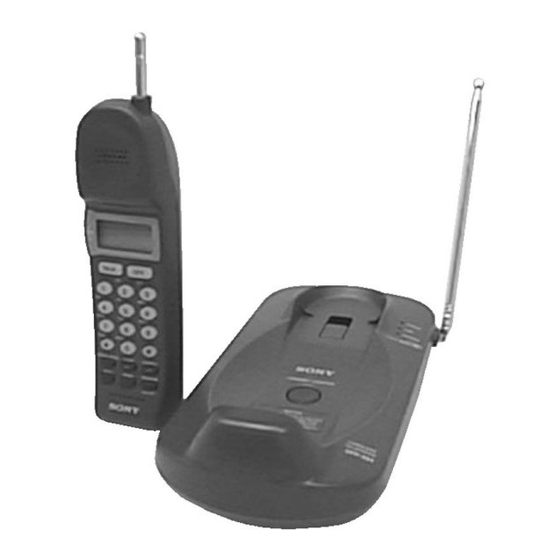
Handset
Power source
Rechargeable battery pack BP-T16
Battery life
Standby : Approx. 14 days
Talk
: Approx. 6 hours
Battery charging time
Approx. 12 hours
Dimensions
Approx. 54 × 195 × 49 mm (w/h/d),
antenna excluded
× 7
× 1
(approx. 2
inches)
1/4
3/4
15/16
Antenna: Approx. 285 mm
(approx. 11
inches)
1/4
Mass
Approx. 240 g (approx. 8 oz), battery
included
MICROFILM
SPP-874/884
Handset
Photo: SPP-884
SPECIFICATIONS
Base unit
Power source
DC 9V from AC power adaptor
Rechargeable battery pack BP-T16
(SPP-884 only)
Battery charging time
Approx. 20 hours (SPP-884 only)
Dimensions
Approx. 120 × 64 × 223 mm (w/h/d),
antenna excluded
(approx. 4
Antenna: Approx. 680 mm
(approx. 26
Mass
Approx. 350 g (approx. 12 oz), wall
bracket and battery excluded
Design and specifications are subject to change without
notice.
• Abbreviation
E12 : 220–240V area of E model
E92 : 120V area of E model
– 1 –
Base unit
× 2
× 8
inches)
3/4
5/8
7/8
inches)
7/8
CORDLESS TELEPHONE
E Model
Advertisement

Related Manuals for Sony SPP-874


Summary of Contents for Sony SPP-874
-
Page 1: Specifications
Approx. 120 × 64 × 223 mm (w/h/d), AC power adaptor (AC-T125) (1) (ARGENTINE) Telephone line cord (1) antenna excluded × 2 × 8 Rechargeable battery pack (BP-T16) (1) (SPP-874) (approx. 4 inches) Rechargeable battery pack (BP-T16) (2) (SPP-884) Antenna: Approx. 680 mm Wall bracket/stand (1) (approx. - Page 2 SPP-874/884 5-4. SCHEMATIC DIAGRAM — BASE SECTION — • Refer to page 37 for IC Block Diagrams. Note: • All capacitors are in µF unless otherwise noted. pF: µµF 50 WV or less are not indicated except for electrolytics and tantalums.
- Page 3 SPP-874/884 5-6. SCHEMATIC DIAGRAM — HAND MAIN SECTION — • Refer to page 37 for IC Block Diagrams. (Page 36) Note: • All capacitors are in µF unless otherwise noted. pF: µµF 50 WV or less are not indicated except for electrolytics and tantalums.
- Page 4 SPP-874/884 5-8. SCHEMATIC DIAGRAM — HAND KEY SECTION — • Refer to page 37 for IC Block Diagrams. (Page 32) Note: • All capacitors are in µF unless otherwise noted. pF: µµF • Voltages are taken with a VOM (Input impedance 10 MΩ).
-
Page 5: Ic Pin Descriptions
• IC Block Diagrams 5-9. IC PIN DESCRIPTIONS • IC801 LC6621108A (SYSTEM CONTROL) (BASE UNIT) Pin No. Pin Name Pin Description RSSI CTRL RSSI sens select output (L: Low sens) IC501 TB31224F (BASE MAIN BOARD) IC1 TB31224F (HAND MAIN BOARD) EEPROM DATA EEPROM data input/output (Not used in this set.) EEROM CLK... - Page 6 CHARGE DET Charge detection input (H: in charge) BAT-LOW-IN Battery low-voltage detection input — — Not used. (Fixed at L (SPP-874/884:E92), H (SPP-884:E12) in this set.) RX-DATA RF reception data input PLL-STB PLL control standby output PLL-DATA PLL control data output...