Table of Contents
Advertisement
Quick Links
Only Oceanian and European
BTDD, STDD
BTPP, STPP
STUA, BTUA
SAFETY-RELATED COMPONENT
WARNING!!
COMPONENTS IDENTIFIED BY MARK
SCHEMATIC DIAGRAM AND IN THE PARTS LIST ARE
CRITICAL FOR RISK OF FIRE AND ELECTRIC SHOCK.
REPLACE THESE COMPONENTS WITH ONKYO
PARTS WHOSE PART NUMBERS APPEAR AS SHOWN
IN THIS MANUAL.
MAKE LEAKAGE-CURRENT OR RESISTANCE
MEASUREMENTS TO DETERMINE THAT EXPOSED
PARTS ARE ACCEPTABLY INSULATED FROM THE
SUPPLY CIRCUIT BEFORE RETURNING THE
APPLIANCE TO THE CUSTOMER.
SERVICE MANUAL
SERVICE MANUAL
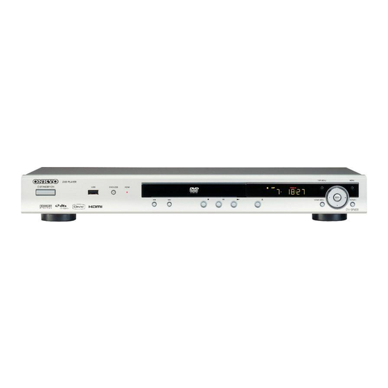
DVD PLAYER
DV-SP405
MODEL
Black and Silver models
120V AC, 60Hz
220-240V AC, 50/60Hz
110-240V AC, 50/60Hz
Ref. No. 4005
North American
ON
STANDBY
OPEN/
CLOSE
PLAY
MODE
1
2
3
DISPLAY
4
5
6
7
8
9
0
CLEAR
TOP MENU
MENU
ENTER
HOME
RETURN
MENU
AUDIO
ANGLE SUBTITLE ZOOM
RC-698DV
RC-698DV
ON THE
DV-SP405
072007
Oceanian and European
ON
STANDBY
OPEN/
CLOSE
PLAY
MODE
1
2
3
DISPLAY
4
5
6
7
8
9
0
CLEAR
TOP MENU
MENU
ENTER
HOME
RETURN
MENU
AUDIO
ANGLE
SUBTITLE ZOOM
DVD/USB
RC-699DV
RC-699DV
Advertisement
Table of Contents

Related Manuals for Onkyo DV-SP405


Summary of Contents for Onkyo DV-SP405
-
Page 1: Dvd Player
COMPONENTS IDENTIFIED BY MARK ON THE SCHEMATIC DIAGRAM AND IN THE PARTS LIST ARE CRITICAL FOR RISK OF FIRE AND ELECTRIC SHOCK. REPLACE THESE COMPONENTS WITH ONKYO PARTS WHOSE PART NUMBERS APPEAR AS SHOWN IN THIS MANUAL. MAKE LEAKAGE-CURRENT OR RESISTANCE... -
Page 2: Specifications
DV-SP405 SPECIFICATIONS NTSC (North American model) Signal System PAL/NTSC (Oceanian and European models) Composite Video Output/Impedance 1.0 V (p-p)/75 ohm negative sync, RCA Y: 1.0 V (p-p)/75 ohm negative sync, 4-pin mini DIN S-Video Output/Impedance (not European model) C: 0.286 V (p-p)/75 ohm Y: 1.0 V (p-p)/75 ohm... - Page 3 DV-SP405 PANEL VIEW Rear Panel North American model Oceanian model European model AUDIO OUTPUT DIGITAL ANALOG COAXIAL...
-
Page 4: Exploded View
DV-SP405 EXPLODED VIEW Only Europe and Oceania models NON-CONTACT SIDE CONTACT SIDE U.S.A. model only Europe/ Oceania Model only... - Page 5 DV-SP405 EXPLODED VIEW DVD MECHANISM Cannot supply separately. If the repair is needed, replace the LOADER SUB ASS'Y. CD2001 PCB610 (LOADING MOTOR PCB ASS'Y) CD2302 Do not replace the parts. Because, minute adjustments are needed if this condition is disassembled further more.
- Page 6 DV-SP405 REMOVAL OF DVD MECHA. PARTS-1 NOTE NOTE 1. Disassemble only the DVD DECK PARTS parts listed here. Minute adjustments are needed if the disassembly 1. In case of the Traverse Ass'y, install it from (1) to (4) in is done. If the repair is needed except listed parts, order.
- Page 7 DV-SP405 REMOVAL OF DVD MECHA. PARTS-2 NOTE 2-4: RACK LOADING/MAIN GEAR/PULLEY GEAR (Refer to Fig. 2-4-A) 1. In case of the Pulley Motor installation, check if the value of the Fig. 2-3-B is correct. 1. Unlock the support and remove the Gear Pulley.
- Page 8 DV-SP405 REMOVAL OF DVD MECHA. PARTS-3 NOTE 1. In case of the Clamper Ass'y installation, install correctly Feed Motor as Fig. 2-5-B. Gear Motor Plate Clamper Check Lock Clamper Traverse Ass'y Gear Feed Fig. 2-5-B 2-6: HOLDER TRAVERSE/INSULATOR (F)/INSULATOR (R) (Refer to Fig. 2-6-A)
-
Page 9: Table Of Contents
WIRING VIEW EUROPEAN AND OCEANIA MODELS OPERATION 1 PCB ASSY LS/RS LS/RS/C/LFE J8002 S-VIDEO OUT S-VIDEO OUT J7301 J7301 OPERATION 3 PCB ASSY OPERATION 2 PCB ASSY (CD601) CP4002 CP601 (CD604) FLDC- DI (M to F) -28V V+3E V+3E FLDC+ DO (F to M) DGND POWER... - Page 10 DV-SP405 CP2301 CVBS/Y/U/V FOCS RTN FOCS RTN J7302 J8001 FOCS DRV FOCS DRV TRKG RTN TRKG RTN TRKG DRV TRKG DRV DRIVE LD_DVD(650) LD_DVD(650) DM-4PB PD/GND PD/GND LD_CD(780) LD_CD(780) VD MT PCB ASSY (1/7–7/7) VR780(CD) VR780(CD) VRCOM VRCOM VR650(DVD) VR650(DVD)
- Page 11 WIRING VIEW OVERALL WIRING CONN NORTH AMERICAN MODEL OPERATION2 OPERATION 1 PCB ASSY PCB ASSY OPERATION3 PCB ASSY (CD601) CP4002 CP601 (CD604) CP605 CP604 FLDC- DI (M to F) -28V V+3E V+3E FLDC+ DO (F to M) DGND POWER POWER DGND V+3E V+3E...
- Page 12 DV-SP405 NNECTION DIAGRAM CP2301 FOCS RTN FOCS RTN FOCS DRV FOCS DRV CVBS/Y/U/V CVBS/Y/U/V S+COAXIAL for ME TRKG RTN TRKG RTN J7302 J7302 J8001 J7301 TRKG DRV TRKG DRV DRIVE DM-4PB LD_DVD(650) LD_DVD(650) PD/GND PD/GND OPTICAL PICK-UP LD_CD(780) LD_CD(780) VR780(CD)
- Page 13 DV-SP405 BLOCK DIAGRAM-1 OVERALL BLOCK DIAGRAM EUROPEAN MODEL EEPROM RESET IC AMP_AUDIO_L/R AUDIO AMP IC IC4001 IC4003 IC8008 S-24CS08AFJ-TB- R3112N291A- RC4580IDR TR-FA 21PIN HNV-08SS44T AMUTE RESET RGB OUT SDA, AUDIO_L, AUDIO_R X4001 27MHz MPEG/MICON 4CH BUS SW IC IC4002 FIP DRIVER IC...
- Page 14 DV-SP405 BLOCK DIAGRAM-2EU DVD LOADER/MPEG BLOCK DIAGRAM LETTER, I/XP, Loader R/CR, B/CB, G/Y, C/V VIDEO DRIVER 6CH IC RESET IC (DM-4) IC7301 IC4003 IOA, V20 SQUEEZE, VSEL1 LA73054-TLM-E R3112N291A RF, A, B, C, D, E, F, MDI1 X4001 CVBS/Y/U/V A, B...
-
Page 15: Fldc
DV-SP405 BLOCK DIAGRAM-3EU POWER BLOCK DIAGRAM PHOTO COUPLER HDMI+5V REG IC504 VOLTAGE CTL IC5902 PS2561AL1-1-V (W) V+5H IC501 PQ1K503M2ZPH KIA431A-AT REG+1.8V POWER CTL IC4006 IC502 +1.8V LM1117S-ADJ STR-A6151M AT+12V for mute Q510 P.CON +12V SW P.CON+12V Q515 P.CON+5V P.CON +5V REG... -
Page 16: Block Diagram
DV-SP405 BLOCK DIAGRAM-1 NORTH AMERICAN MODEL OVERALL BLOCK DIAGRAM EEPROM RESET IC AMP_AUDIO_L/R AUDIO AMP IC IC4001 IC4003 IC8008 S-24CS08AFJ-TB- R3112N291A- RC4580IDR TR-FA HNV-08SS44T AUDIO_L, AMUTE RESET SDA, SCL AUDIO_R X4001 27MHz MPEG/MICON IC4002 FIP DRIVER IC FP,STB AUDIO CODEC/... - Page 17 DV-SP405 BLOCK DIAGRAM-2US DVD LOADER/MPEG BLOCK DIAGRAM S+COAXIAL J7301 LETTER, I/XP, Loader RESET IC R/CR, B/CB, G/Y, CVBS VIDEO DRIVER 6CH IC (DM-4) IC4003 IC7301 IOA, V20 R3112N291A- SQUEEZE, VSEL1 LA73054-TLM-E TR-FA RF, A, B, C, D, E, F, MDI1...
-
Page 18: Power Block Diagram
DV-SP405 BLOCK DIAGRAM-3US POWER BLOCK DIAGRAM PHOTO COUPLER IC504 VOLTAGE CTL PS2561AL1-1-V (W) IC501 KIA431A-AT REG+1.8V POWER CTL IC4006 IC502 +1.8V LM1117S-ADJ STR-A6131M AT+12V for mute Q510 P.CON +12V SW P.CON+12V Q515 P.CON+5V P.CON +5V REG 6V REG SWITCHING P.CON+6V... - Page 19 SCHEMATIC DIAGRAM-1 EU DVD MT PCB ASSY (1/7) MPEG/MICON/RF-AMP BLOCK FROM/TO LOADER/MOTOR DRV X4001 100GT02720 27MHz R4025 R4057 100K C4033 C4047 0.001 B 0.001 B R4048 R4026 PLLVDD3 R4024 R4053 0.01 W816 RFVDD3 750K MDI1 LDO1 LDO2 V1P4 C4028 DMSO FMSO 0.1 B 1.6 1.8...
-
Page 20: V+3E
DV-SP405 C4011 LETTER ASPDIF SQUEEZE YK_P I/XP C4128 R/CR B/CB 0.01 B CVBS R4061 D_GND D_GND R4002 FROM/TO POWER PORT 0 0 0 0 3.2 3.2 3.2 0 3.1 3.2 3.2 2.9 2.8 3.2 3.3 3.3 3.2 1.0 1.0 2.2K +-1%... - Page 21 SCHEMATIC DIAGRAM-2 EU DVD MT PCB ASSY (2/7) MEMORY BLOCK 16Mbit FLASH IC IC4004 ES29LV160EB-70TG FROM/TO MPEG/MICON/DSP BYTE# D15/A1 DQ10 DQ11 DQ12 DQ13 DQ14 DQ15 R4044 MA10 PWR# MA11 DWE# C4062 SDCKE RESET# DQM1 0.001 B DQM0 DCAS# C4040 DRAS# DBA1 DBA0 NC (WP#/ACC)
- Page 22 DV-SP405 When ordering service parts, be sure to refer to "EXPLODED VIEWS and PARTS LIST" or "PCB PARTS LIST". The > mark found on some component parts indicates the importance of the safety factor of the part. Therefore, when replacing, be sure to use parts of identical designation.
- Page 23 SCHEMATIC DIAGRAM-3 EU LOADER/MOTOR DVR BLOCK DVD MT PCB ASSY (3/7) C2303 0.1 B PICK-UP(GOLD) V+5S CP2301 C2301 0.1 B LD07T2-24ND-03 TP2304 TP2305 TP2306 R2307 TP2307 VCR_CTL TP2308 Q2307 100K KTK5132U-RTK/P TP2309 SW1(DVD/CD) TP2302 VCR_CTL VRF(RF_OUT) R2309 VCR_CTL TP2310 Q2306 Q2301 KTK5132U-RTK/P TP2311...
- Page 24 DV-SP405 FROM/TO MPEG/MICON/DSP RF33 JG010 TP2332 JG008 TP2341 V+3F MDI1 LDO2 LD DRIV for CD LDO1 LD DRIV for CD Q2304 LDO1 Q2302 KTA1504S_Y_RTK KTA1504S_Y_RTK V1P4 LIMIT TROUT TRIN STBY JG009 DMSO TP2342 FMSO TRCLOSE TROPEN LD DRIV for DVD...
- Page 25 SCHEMATIC DIAGRAM-4 EU AUDIO/JACK BLOCK DVD MT PCB ASSY (4/7) FROM MPEG/MICON/RF-AMP XAMUTE ASPDIF FROM POWER PORT V+12 V+12AT D_GND TO VIDEO AUDIO_L AUDIO_R COAXIAL MUTE CTL Q8012 KTA1504S_Y_RTK R8038 V+12AT 6.8K V+12 R8023 MUTE CTL R8020 XAMUTE 6.8K Q8007 KRC407-RTK/P 2.2K C8011...
- Page 26 DV-SP405 R8016 2.4K C8074 COAXIAL for ME COAXIAL DRIV J8003 Q8025 RCA-125-01 KTC3875S_Y_RTK R8089 C8066_1 KA_P R8082 220 +-1% R8059 -0.7 MUTE SW R8085 27K +-1% Q8019 KTC2875-B R8043 R8043 R8061 10K +-1% 10K +-1% 10K +-1% R8042 R8042 C8069...
-
Page 27: Cvbs
SCHEMATIC DIAGRAM-5 EU DVD MT PCB ASSY (5/7) VIDEO BLOCK VIDEO DRIVER 6CH IC IC7301 LA73054 VCC1 AMP1 (9dB=H,6dB=L) C7305 CVBS CVBS in DRIVE1 (1D=H,2D=L) C7302 SQUEEZE VCC21 0.1 B LETTER CVBS out FROM AUDIO/JACK MUTE1 GND21 (ON=H,OFF=L) AUDIO_L C7304 C in C out AUDIO_R... - Page 28 DV-SP405 FROM/TO POWER VIDEO/AUDIO for 21PIN CP7301 IMSA-9604S-12C 21PIN-G/D-Y 21PIN-B/D-U 21PIN-R/D-V P-H/I-L_RGB-H RGB-H ASP/FS CVBS AUDIO L AUDIO R TP7301 CVBS 4CH BUS SW IC IC7302 SN74CBT3257PWR CVBS/Y/U/V J7302 RCA-405A-08 CAUTION: DIGITAL TRANSISTOR...
- Page 29 SCHEMATIC DIAGRAM-6 EU HDMI BLOCK DVD MT PCB ASSY (6/7) FROM POWER PORT V+5H D_GND FROM/TO MPEG/MICON/DSP TX2+ TX2- TX1+ TX1- TX0+ TX0- TXC+ TXC- HDMI_SCL HDMI_SDA W855 A_GND W856 W861 L5901~590 L5901~590 TX2+ TX2+ TX2- TX2- TX1+ TX1+ TX1- TX1- TX0+ TX0+...
- Page 30 DV-SP405 ~5904 C ~5904 CLOSED TO CP5901 L5901 EXC24CG900U W857 W850 W862 MP MODIFY HDMI CONNECTOR L5902 CP5901 EXC24CG900U 1903015-3 TX2+ D2-S TX2+ TX1+ L5903 D1-S EXC24CG900U TX1- TX0+ D0-S TX0- TXC+ CLK+ L5904 CLK-S EXC24CG900U TXC- CLK- HDMI_S HDMI_SCL...
-
Page 31: P.con+12V
SCHEMATIC-DIAGRAM-7 EU DVD MT PCB ASSY (7/7) POWER PORT BLOCK REG+1.8V IC IC4006 LM1117S-ADJ MP MODIFY VOUT W843 W820 R4011 R4012 68 +-1% FROM/TO POWER CP4003 (CP502) A2001WV2-14P P.CON+12V AT+12V for MUTE P.CON+5V P.CON+6V GND(M) AT+3.3V +3.3V TP4064 AT+3.3V STBY L GND(D) FL DC- FL DC+... - Page 32 DV-SP405 TO AUDIO/VIDEO/JACK V+3A (VIDEO/OPT/COAX) (AUDIO MUTE) V+12AT V+12AT B4002 V+12 (AUDIO AMP) V+12 MMZ1608R102CT D_GND ADACVDD REG Q4001 KTC3875S_Y_RTK W824 TO LOADER/MOTOR DRV V+6A (MOTOR) V+6A B4001 V+5S (OPU) V+5S MMZ1608R102CT (F/E) V+3F V+3F HDMI+5V REG(300mA) IC W839 D_GND...
- Page 33 SCHEMATIC DIAGRAM-8 EU V651 HNV-08SS44T DVD CD TRACK RACK OPERATION 1 and OPERATION 2 PCB ASSYS OPERATION 1 PCB ASSY D651 1SS133 D652 1SS133 OPERATION 3 PCB ASSY D654 1SS133 D655 1SS133 D656 1SS133 (OPERATION3 PCB) D657 1SS133 D658 1SS133 D659 1SS133 D665...
- Page 34 DV-SP405 CK ALL CK ALL REPEAT A FLDC- W805 FLDC+ Switches SW652 : DOWN SW653 : ENTER SW654 : RIGHT SW655 : RETURN SW656 : MENU SW657 : UP SW658 : TOPMENU SW659 : LEFT SW660 : STOP -28V SW661 : HOMEMENU...
-
Page 35: Power Block
SCHEMATIC DIAGRAM-9 EU POWER PCB ASSY (1/2) POWER BLOCK CHASSIS GND PRIMARY side D505 1N4005-EIC D502 1N4005-EIC D503 51MS016L 1N4005-EIC F501 T1.6A_L_250V D506 AC220V-240V_50Hz/60Hz(EU) COIL,LINE FILTER 1N4005-EIC CD501_2 L501 FH501 FH502 06158802 SS11V-03550-CH EYF-52BCY EYF-52BCY PAL/NTSC AC INLET J501 YKE31-0148N -22.5 -22.5 T501... -
Page 36: At+12V For Mute
DV-SP405 P.CON+12V SW Q510 KTA1281_Y W817 FROM USB PCB 12.9 12.6 USB POWER 12.3 +5.2V REG (USB) CP504 IC505 A2001WV2-4P PQ070XF01SZH 12.3 REG+12V CTL USB+5V 12.9 D512_1 D512_1 Q509 USB+5V KTC3875S_Y_RTK 1H3-E 1H3-E REG+12V CTL Q511 KTC3875S_Y_RTK +6V REG (DVD MOTOR) - Page 37 SCHEMATIC DIAGRAM-10 EU POWER PCB ASSY (2/2) 21 PIN/D-TERMINAL/DIGITAL BLOCK FROM POWER B8103 P.CON+D5V MMZ1608R102CT AT+3.3V P.CON+12V P-H/I-L_RGB-H ASP/FS AMP_A_OUT_R AMP_A_OUT_L G/Y_VIDEO B/U_VIDEO R/V_VIDEO CVBS/C_VIDEO A_GND 12.1 21PIN CTL IN 21PIN CTL DRV R8105 11.4 Q8102 Q8101 390 1/4W KTA1504S_Y_RTK KTC3875S_Y_RTK 11.4 12.1...
- Page 38 DV-SP405 21PIN CONNECTOR J8101 MRC-021V-07_A R8114 21PIN_R 220 +-1% R8115 21PIN_L +-1% L8101 21PIN_CTL 10uH 0405 C8112 R8110 G/Y_VIDEO_OUT 6.3V 1000 YK_P +-1% C8113 R8111 B/U_VIDEO_OUT 6.3V YK_P +-1% C8114 R8112 R/V_VIDEO_OUT 6.3V YK_P +-1% BLANKING_OUT C8115 R8113 CVBS_VIDEO_OUT +-1% 6.3V...
-
Page 39: P.con+5V
SCHEMATI DIAGRAM-11 EU USB PCB ASSY FROM/TO DVD PCB CP6601 00_6232_006_102_800+ USB_P_ON-H USB_POWER USB_FLAG USB_FLAG USBP USBP USBN USBN CORD CONNECTOR CD6601 HIGH SIDE SW IC (60 OHM 2.5A) IC6601 RT9702-PB (SCHO 2H063401 B6601 VOUT HCB2012K-600T25 TO POWER PCB CP6602 A2001WR2-4P P.CON+5V /FLG... - Page 40 DV-SP405 SCHOTTKY 3.0A) (60 OHM 2.5A) D6601 B6602 HCB2012K-600T25 RB051L-40 CP6603 USB-A1D05F-4B4N W809 USB_DN W810 USB_DP C6610 W801 100P CH NOTE:THE DC VOLTAGE AT EACH PART WAS MEASURED WITH THE DIGITAL TESTER WHEN THE COLOR BROADCAST WAS RECEIVED IN GOOD CONDITION AND PICTURE IS NORMAL.
- Page 41 SCHEMATIC DIAGRAM-1 US MPEG/MICON/RF-AMP DVD MT PCB X4001 ASSY (1/7) 100GT02720 27 MHz R4025 100K C4033 R4057 FROM/TO LOADER/MOTOR DRV 0.001 C4047 0.001 B R4048 R4026 PLLVDD3 R4024 R4053 W816 RFVDD3 750K MDI1 LDO1 LDO2 V1P4 C4028 0.1 B DMSO FMSO N NC TRCLOSE...
- Page 42 DV-SP405 MPEG/MICON/RF-AMP TO VIDEO VSEL1 C4011 LETTER SQUEEZE TO AUDIO/JACK I/XP YK_P R/CR B/CB C4128 CVBS 0.01 B XAMUTE ASPDIF R4061 D_GND R4002 D_GND FROM/TO POWER PORT 2.2K +-1% R4064 150 +-1% TP4060 ADAC_GND V+5H C4074 0.1 B R4065 150 +-1%...
- Page 43 SCHEMATIC DIAGRAM-2 US DVD MT PCB ASSY (2/7) MEMORY SCHEMATIC DIAGRAM (DVD MT PCB) 16Mbit FLASH IC IC4004 ES29LV160EB-70TG FROM/TO MPEG/MICON/DSP BYTE# D15/A1 DQ10 DQ11 DQ12 DQ13 DQ14 DQ15 R4044 MA10 PWR# MA11 DWE# C4062 SDCKE RESET# DQM1 0.001 B DQM0 C4040 DCAS#...
- Page 44 DV-SP405 ÷ When ordering service parts, be sure to refer to "EXPLODED VIEWS and PARTS LIST" or "PCB PARTS LIST". ÷ The > mark found on some component parts indicates the importance of the safety factor of the part. Therefore, when replacing, be sure to use parts of identical designation.
- Page 45 SCHEMATIC DIAGRAM-3 US LOADER/MOTOR DRIVE DVD MT PCB C2303 0.1 B ASSY (3/7) PICK-UP(GOLD) V+5S CP2301 C2301 0.1 B LD07T2-24ND-03 TP2304 TP2305 TP2306 R2307 TP2307 VCR_CTL TP2308 Q2307 100K KTK5132U-RTK/P TP2309 SW1(DVD/CD) TP2302 VCR_CTL R2309 VRF(RF_OUT) TP2310 VCR_CTL Q2306 Q2301 KTK5132U-RTK/P TP2311 KTC3875S_Y_RTK...
-
Page 46: Gnd(M)
DV-SP405 (DVD MT PCB) FROM/TO MPEG/MICON/DSP RF33 JG010 TP2332 JG008 TP2341 V+3F MDI1 LDO2 LD DRIV for CD LDO1 LD DRIV for CD Q2304 LDO1 Q2302 KTA1504S_Y_RTK KTA1504S_Y_RTK V1P4 LIMIT TROUT TRIN STBY JG009 DMSO TP2342 FMSO TRCLOSE TROPEN LD DRIV for DVD... - Page 47 SCHEMATIC DIAGRAM-4 US DVD MT PCB ASSY (4/7) AUDIO/JACK SCHEMATIC DIAGRAM FROM MPEG/MICON/RF-AMP XAMUTE ASPDIF FROM POWER PORT V+12 V+12AT D_GND TO VIDEO COAXIAL MUTE CTL Q8012 KTA1504S_Y_RTK R8038 6.8K V+12AT MP MODIFY V+12 MUTE CTL XAMUTE R8023 6.8K Q8007 KRC407-RTK/P R8020 2.2K R8100...
- Page 48 DV-SP405 (DVD MT PCB) R8016 2.4K C8074 COAXIAL DRIV Q8025 KTC3875S_Y_RTK R8089 C8066_1 KA_P R8059 27K +-1% R8043 R8061 10K +-1% 10K +-1% R8042 C8011 C8011 R8100 C8069 R8087 R8096 TP8017 NA_P 470K 220 +-1% 220 +-1% YK_P -0.7 R8088...
- Page 49 SCHEMATIC DIAGRAM-5 US VIDEO SCHEMATIC DVD MT PCB ASSY (5/7) VIDEO DRIVER 6CH IC IC7301 LA73054-TLM-E VCC1 AMP1 (9dB=H,6dB=L) C7305 CVBS CVBS in DRIVE1 (1D=H,2D=L) C7302 SQUEEZE VCC21 0.1 B LETTER CVBS out MUTE1 GND21 (ON=H,OFF=L) C7304 FROM AUDIO/JACK C in C out COAXIAL W877...
- Page 50 DV-SP405 (DVD MT PCB) TP7301 CVBS J7302 J7301 RCA-405A-08 S+COAXIAL for ME CVBS/Y/U/V R102-D04KA(III)-06 CAUTION: DIGITAL TRANSISTOR...
- Page 51 SCHEMATIC DIAGRAM-6 US DVD MT PCB ASSY (6/7) HDMI SCHEMATIC (DVD MT FROM POWER PORT V+5H D_GND FROM/TO MPEG/MICON/DSP TX2+ TX2- TX1+ TX1- TX0+ TX0- TXC+ TXC- HDMI_SCL HDMI_SDA W855 A_GND W856 W861 A_GND NOTE:THE DC VOLTAGE EACH PART WAS MEASURED WITH THE DIGITAL TESTER DURING PLAYBACK.
- Page 52 DV-SP405 MT PCB) L5901~5904 CLOSED TO CP5901 TX2+ EXC24CG900U L5901 TX2- W857 W850 TX1+ W862 MP MODIFY HDMI CONNECTOR EXC24CG900U CP5901 L5902 1903015-3 TX1- TX2+ D2-S TX2+ TX0+ TX1+ EXC24CG900U D1-S L5903 TX1- TX0- TX0+ D0-S TX0- TXC+ TXC+ CLK+...
-
Page 53: At+3.3V
SCHEMATIC DIAGRAM-7 US POWER PORT SCHEMATIC DVD MT PCB ASSY (7/7) (DVD MT PCB) REG+1.8V IC IC4006 LM1117S-ADJ MP MODIFY VOUT W843 W820 R4011 R4012 68 +-1% FROM/TO POWER (CP502) CP4003 A2001WV2-14P P.CON+12V AT+12V for MUTE P.CON+5V P.CON+6V GND(M) AT+3.3V +3.3V TP4064 AT+3.3V... - Page 54 DV-SP405 TO AUDIO/VIDEO/JACK (VIDEO/OPT/COAX) V+12AT (AUDIO MUTE) V+12AT B4002 (AUDIO AMP) V+12 V+12 MMZ1608R102CT D_GND ADACVDD REG Q4001 KTC3875S_Y_RTK W824 TO LOADER/MOTOR DRV V+6A (MOTOR) V+6A B4001 V+5S (OPU) V+5S MMZ1608R102CT V+3F (F/E) V+3F HDMI+5V REG(300mA) IC W839 D_GND IC5902...
- Page 55 SCHEMATIC DIAGRAM-8 US OPERATION 1 and OPERATION 2 and OPERATION 3 PCB ASSYS Switches SW652 : DOWN ( ) OPERATION 1 PCB ASSY SW653 : ENTER (OPER SW654 : RIGHT ( ) V651 HNV-08SS44T SW655 : RETURN DVD CD TRACK ALL SW656 : MENU SW657 : UP ( ) SW658 : TOP MENU...
- Page 56 DV-SP405 DISPLAY SCHEMATIC DIAGRAM PERATION PCB) FLDC- W805 FLDC+ -28V -19.0 -15.6 R651 R652 FP_SCK R653 FP_DI R654 FP_DO R662 100K LED4 LED3 LED2 LED1 0 -16.0 -16.0 FROM/TO MPEG/MICON/RF-AMP CP601 (CP4002) 00_6232_011_102_800+ FP_SCK FP_DI DI (M to F) FP_DO...
- Page 57 SHEMATIC DIAGRAM-9 US POWER SCHEMATIC DIAGRAM (POWER POWER PCB ASSY CHASSIS GND PRIMARY side AC 120 V_60 Hz (US) CD501 0Q618902 D505 CP501 A3963WV2-3PD 1N4005-EIC CONNECTOR NTSC WHITE(N) D502 WHITE 1N4005-EIC BLACK BLACK(L) T501 81291294 D503 1N4005-EIC F501_1 1.6A125V D506 L501 1N4005-EIC SS11V-03550-CH...
-
Page 58: P.on-H
DV-SP405 WER PCB) P.CON+12V SW Q510 KTA1281_Y W817 12.9 12.6 12.3 12.3 REG+12V CTL 12.9 D512_1 D512_1 Q509 KTC3875S_Y_RTK 1H3-E 1H3-E REG+12V CTL Q511 KTC3875S_Y_RTK +6V REG (DVD MOTOR) IC IC503 PQ070XF01SZH R546 R545 22K +-1% 3.3K 1/4W FROM/TO POWER PORT... -
Page 59: Power Pcb Assy
DV-SP405 WAVE FORMS-1 EU European and Oceania models Note : The encircled numbers denote measuring point in the schematic diagram. POWER PCB ASSY DVD MT PCB ASSY 21PIN/D-TERMINAL/DIGITAL AUDIO MPEG/MICON/RF AMP J8003-pin2 (Coaxial_Out) IC4002-pin146 (RCLK) J8101-pin11 (G/Y_Video_Out) V:500mV/div. H:200nsec/div. V:1.0V/div. H:2nsec/div. - Page 60 DV-SP405 WAVE FORMS-2 EU European and Oceania models Note : The encircled numbers denote measuring point in the schematic diagram. POWER PCB ASSY 21PIN/D-TERMINAL/DIGITAL AUDIO J8101-pin3 (AMP_A_Out_L)) V:1.0V/div. H:200µsec/div. OPERATION 1 PCB ASSY DISPLAY IC651-pin5 (OSC) V:500mV/div. H:1µsec/div.
- Page 61 DV-SP405 WAVE FORMS-US North American model Note : The encircled numbers denote measuring point in the schematic diagram. DVD MT PCB ASSY MPEG/MICON/DSP J7301-pin3 (S_Y) IC4002-pin136 (RCLK) J8002-pin2 (Coaxial_Out) V:1.0V/div. H:2nsec/div. V:500mV/div. H:20µsec/div. V:500mV/div. H:200nsec/div. IC4002-pin215 (ASPDIF) J7302-pin6 (CVBS_Out) J7301-pin4 (S_C) V:1.0V/div.
- Page 62 DV-SP405 PACKING VIEW Battery European and Oceanian models European model U.S.A. only...
- Page 63 DV-SP405 PRINTED CIRCUIT BPARD VIEW-1 DVD MT PCB ASSY SIDE A SIDE A DVD MT PCB ASSY (TOP SIDE) W851 C4050 IC4001 IC4005 R5919 L5904 NR4001 C4104 R5920 L5903 L5902 L5901 NR4002 W850 C4114 R4083 R4059 R4007 B7305 R4021 R4082...
- Page 64 DV-SP405 PRINTED CIRCUIT BPARD VIEW-2 DVD MT PCB ASSY SIDE B SIDE B DVD MT PCB ASSY (BOTTOM SIDE) R4044 R4051 Q4004 Q4002 R4003 W816 W864 R4064 D7310 R4065 R4026 R2327 R7304 W807 Q7302 R8004 R8086 Q8025 W822 R4058 R8084...
- Page 65 DV-SP405 PRINTED CIRCUIT BOARD VIEW-3 SIDE A OPERATION 1 PCB and SW655 SIDE A OPERATION 2 PCB ASSYS SW656 SW654 SW652 SW653 SW659 W809 SW661 SW658 W007 W009 W003 C658 C605 C604 C675 D669 R662 R654 W011 W012 W013 R653...
- Page 66 DV-SP405 PRINTED CIRCUIT BOARD VIEW-4 POWER PCB ASSY SIDE A SIDE A POWER PCB ASSY (INSERTED PARTS) SOLDER SIDE D503 C511 D506 F501 FH501 FH502 D502 D511 C502_1 D505 PH503 IC502 D509 IC505 C505 D508 C504 R546 C530 C506 W038...
- Page 67 DV-SP405 PRINTED CIRCUIT BOARD VIEW-5 POWER PCB ASSY SIDE A SIDE A POWER PCB ASSY (CHIP MOUNTED PARTS) SOLDER SIDE...
-
Page 68: Load
DV-SP405 PRINTED CIRCUIT BOARD VIEW-6 USB PCB, LOADING MOTOR and SW ASSYS SIDE A SIDE A LOADING MOTOR (INSERTED PARTS) USB (CHIP MOUNTED PARTS) SOLDER SIDE SOLDER SIDE DED021A D6608_1 D6610_1 C6609 W809 C6608 B6602 C6610 W801 R6613 W810 C6604... -
Page 69: Open
DV-SP405 IC BLOCK DIAGRAM/ TERMINAL DESCRIPTIONS-1 • The information shown in the list is basic information and may not correspond exactly to that shown in the schematic diagrams. MT1389FE/E-L (DVD MT PCB ASSY: IC4002) • MPEG / MICON / DSP •... - Page 70 DV-SP405 IC BLOCK DIAGRAM/ TERMINAL DESCRIPTIONS-2 • MPEG / MICON / DSP Microcomputer • Block Diagram Debug CVBS, Y/C 108Mhz Component Port TV Encoder Module Videop RF Amplifier Video DAC Servo IO Servo Motor Processor Video Drive Processor interlacer Spindle...
- Page 71 DV-SP405 IC BLOCK DIAGRAM/ TERMINAL DESCRIPTIONS-3 • Pin Function...
- Page 72 DV-SP405 IC BLOCK DIAGRAM/ TERMINAL DESCRIPTIONS-4...
- Page 73 DV-SP405 IC BLOCK DIAGRAM/ TERMINAL DESCRIPTIONS-5...
- Page 74 DV-SP405 IC BLOCK DIAGRAM/ TERMINAL DESCRIPTIONS-6...
- Page 75 DV-SP405 IC BLOCK DIAGRAM/ TERMINAL DESCRIPTIONS-7...
- Page 76 DV-SP405 IC BLOCK DIAGRAM/ TERMINAL DESCRIPTIONS-8...
- Page 77 DV-SP405 IC BLOCK DIAGRAM/ TERMINAL DESCRIPTIONS-9...
- Page 78 DV-SP405 IC BLOCK DIAGRAM/ TERMINAL DESCRIPTIONS-10...
- Page 79 DV-SP405 IC BLOCK DIAGRAM/ TERMINAL DESCRIPTIONS-11...
- Page 80 DV-SP405 IC BLOCK DIAGRAM/ TERMINAL DESCRIPTIONS-12 Note: 1. The Main column is the main function, Alt. means alternative function. 2. The external TV encoder mode only supports CCIR-656 mode.
- Page 81 DV-SP405 SERVICE PROCEDURES-1 NOTES ON SOLDERING • For environmental protection, lead-free solder is used on the printed circuit boards mounted in this unit. • Be sure to use lead-free solder and a soldering iron that can meet specifications for use with lead-free solders for repairs accompanied by reworking of soldering.
-
Page 82: Disc Removal Method
DV-SP405 SERVICE PROCEDURES-2 DISC REMOVAL METHOD DISC REMOVAL METHOD AT NO POWER SUPPLY Slide the Rack Loading (White) toward the arrow direction by using a minus driver to release the lock. (Refer to Fig. 1) Manually open the Tray. NOTE: Please strongly pushing Rack Loading (White) to release the lock because the tray doesn't go out easily. - Page 83 DV-SP405 SERVICE PROCEDURES-3 RESETTING THE PLAYER. (Factory default) 1. Switch the player into standby. 2. Using the front panel buttons, fold down the (stop) button and press STANDBY/ON to switch the player back on. TRAY LOCK MODE 1. While standby on, press “SKIP +”, “SKIP -” and “STOP” key at the same time.
- Page 84 DV-SP405 FIRMWARE DOWN LOADING HOME MENU Confirm the Regional code and Firmware version. 1. Connect the TV monitor to the DV-SP405. Audio Settings Video Adjust 2. Turn ON the standby switch ON. (No Disc) 3. Press "SET UP" key of remote controller (RC-574DV).
-
Page 85: Trouble Shooting
DV-SP405 TROUBLE SHOOTING-1 POWER DOES NOT TURN ON Is the voltage at Check AT+3.3V line of POWER BLOCK. pin 8 and pin 9 of CP502 about 3.3V and at pin 5 of CP502 Check Q515 and peripheral circuit. about 5V? - Page 86 DV-SP405 TROUBLE SHOOTING-2 DOES NOT LIGHT ON DISPLAY Is the voltage at Check AT+3.3V line of pin 13 and pin 43 of IC651 POWER BLOCK. about 3V ? Replace V651 or IC651. NO PLAYBACK PICTURE OF AV JACK Is there...
- Page 87 DV-SP405 TROUBLE SHOOTING-3 NO DIGITAL AUDIO ON PLAYBACK OF COAXIAL JACK Is there Check connection at RCA waveform at pin 2 of J8001 Cable. about 0.3Vp-p? Is there Check Q8025 and waveform at pin 215 of IC4002 peripheral circuit. about 0.3Vp-p ? Change IC4002.
- Page 88 DV-SP405 TROUBLE SHOOTING-4 Symptoms That May Occur When Any Of The Following ICs Is In Failure EEPROM User's data cannot be stored in memory. (DVD MT PCB Assy : IC4001) The ID number is lost. 16M Flash ROM The power cannot be turned on.
-
Page 89: Parts List
PARTS LIST DV-SP405 NOTE: NSP: Not service parts <STDD>: Silver/U.S.A. model <BTDD>: Black/U.S.A. model <STPP>: Silver/ European model <BTPP>: Black/ European model <B>: Black color <S>: Silver color : Safety parts EXPLODED VIEW PARTS LIST PARTS NAME PART NO. REMARKS... - Page 90 SHEET FUSE 7240001122 <TUA> SCREW PAN 810213060U FLAP DVD 712WPDA081 Door, Revision (08/JAN/17) DV-SP405 PACKING VIEW PARTS LIST PARTS NAME PART NO. REMARKS RCA PIN CABLE 06CPBA2006 TRANSMITTER 07660LP020 Remote controller <TDD> TRANSMITTER 07660LP030 Remote controller <TPP><TUA> INSTRUCTION BOOK J2K41701A...
- Page 91 811022680U 2.6 x 8 SEMS.TAP TITE(P) PAN 816112080U 2 x 8 SCREW,TAP TITE(P) BI 811022080U 2 x 8 DVD MECHA. ASSY A2K001A650 DV-SP405 PRINTED CIRCUIT BOARD PARTS LIST PARTS NAME PART NO. REMARKS DVD MT PCB A2K417A130 <TDD> A2K419A130 <TPP>...
- Page 92 Sales & Product Planning Div. : 2-1, Nisshin-cho, Neyagawa-shi, OSAKA 572-8540, JAPAN Tel: 072-831-8023 Fax: 072-831-8124 ONKYO U.S.A. CORPORATION 18 Park Way, Upper Saddle River, N.J. 07458, U.S.A. Tel: 201-785-2600 Fax: 201-785-2650 http://www.us.onkyo.com/ ONKYO EUROPE ELECTRONICS GmbH Liegnitzerstrasse 6, 82194 Groebenzell, GERMANY Tel: +49-8142-4401-0 Fax: +49-8142-4401-555 http://www.eu.onkyo.com/...
Need help?
Do you have a question about the DV-SP405 and is the answer not in the manual?
Questions and answers