Table of Contents
Advertisement
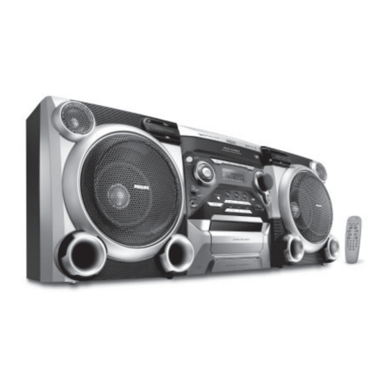
Mini System
©
Copyright 2007 Philips Consumer Electronics B.V. Eindhoven, The Netherlands
All rights reserved. No part of this publication may be reproduced, stored in a retrieval system or
transmitted, in any form or by any means, electronic, mechanical, photocopying, or otherwise without
the prior permission of Philips.
Published by SL0706 Service Audio
Version 1.0
TABLE OF CONTENTS
Specifi cations .............................................................. 1-1
Measurement Setup .................................................... 1-2
Service Aids, Safety Instruction, etc ..................1-3 to 1-6
Block Diagram ................................................................ 2
Wiring Diagram ............................................................... 3
Front Board & USB Board .............................................. 4
Cpu/Wma Board ............................................................ 5
Main Board & Power Board ............................................ 6
Amp (Low Power) Board ................................................ 7
Mechanical Exploded View & Parts List ......................... 8
Printed in The Netherlands Subject to modifi cation.
FWM377/
Page
CLASS 1
LASER PRODUCT
GB
05/12/55
3141 785 31630
Advertisement
Table of Contents

Related Manuals for Philips FWM377/05/12/55


Summary of Contents for Philips FWM377/05/12/55
- Page 1 LASER PRODUCT © Copyright 2007 Philips Consumer Electronics B.V. Eindhoven, The Netherlands All rights reserved. No part of this publication may be reproduced, stored in a retrieval system or transmitted, in any form or by any means, electronic, mechanical, photocopying, or otherwise without the prior permission of Philips.
- Page 2 SPECIFICATION TAPE PLAYER AMPLIFIER Frequency response RMS output power Normal tape (type I) ..125 – 8000 Hz (8 dB) 1KHz (Low channel-both channels driven) ..............60 W per channel Signal-to-noise ratio 10KHz (High channel-both channels driven) ..Normal tape (type I) ......... 48 dB A .............
-
Page 3: Measurement Setup
MEASUREMENT SETUP Tuner FM Bandpass LF Voltmeter 250Hz-15kHz e.g. PM2534 e.g. 7122 707 48001 RF Generator e.g. PM5326 S/N and distortion meter e.g. Sound Technology ST1700B Use a bandpass filter to eliminate hum (50Hz, 100Hz) and disturbance from the pilottone (19kHz, 38kHz). Tuner AM (MW,LW) Bandpass LF Voltmeter... - Page 4 SERVICE AIDS ESD Equipment: Service Tools: Anti-static table mat - large 1200x650x1.25mm ...4822 466 10953 Universal Torx driver holder .........4822 395 91019 anti-static table mat - small 600x650x1.25mm ..4822 466 10958 Torx bit T10 150mm ...........4822 395 50456 Anti-static wristband ..........4822 395 10223 Torx driver set T6-T20 .........4822 395 50145 Ω) Connectorbox (1M...
-
Page 5: Laser Product
WAARSCHUWING WARNING Alle IC’s en vele andere halfgeleiders zijn All ICs and many other semi-conductors are gevoelig voor electrostatische ontladingen susceptible to electrostatic discharges (ESD). (ESD). Careless handling during repair can reduce life Onzorgvuldig behandelen tijdens reparatie kan drastically. de levensduur drastisch doen verminderen. When repairing, make sure that you are Zorg ervoor dat u tijdens reparatie via een connected with the same potential as the mass... - Page 6 To avoid wear-out of tips switch off un-used equipment, or reduce heat. • Mix of lead-free solder alloy / parts with leaded solder alloy / parts is possible but PHILIPS recommends strongly to avoid mixed solder alloy types (leaded and lead-free).
- Page 7 SET BLOCK DIAGRAM...
- Page 8 SET WIRING DIAGRAM...
- Page 9 FRONT & USB BOARD TABLE OF CONTENTS Front PCB - Layout Top View .......... 6-2 Front PCB - Layout Bottom View ........6-3 Front & USB PCB - Circuit Diagram ......... 6-4 USB PCB - Layout ............6-5...
- Page 10 PCB LAYOUT - FRONT BOARD (TOP VIEW)
- Page 11 PCB LAYOUT - FRONT BOARD (BOTTOM VIEW)
- Page 12 CIRCUIT DIAGRAM - FRONT BOARD...
- Page 13 PCB LAYOUT - USB BOARD...
- Page 14 CPU/WMA BOARD TABLE OF CONTENTS CPU/WMA PCB - Layout Top View ......... 5-2 CPU/WMA PCB - Layout Bottom View ......5-3 CPU/WMA PCB - Circuit Diagram ......5-4 to 5-10...
- Page 15 PCB LAYOUT - CPU/WMA BOARD (TOP VIEW)
- Page 16 PCB LAYOUT - CPU/WMA BOARD (BOTTOM VIEW)
- Page 17 CIRCUIT DIAGRAM - CPU/WMA BOARD WMA5250 Module&USB2.0 Host FB1 2K7@100MHz FB2 2K7@100MHz 1.2V FB3 2K7@100MHz MAIN_VCC FB=Ferrite Bead Package 0603 0.1uF 0.1uF 0.1uF 0.1uF 0.1uF 0.1uF 0.1uF 680pF 0.1uF 680pF MAIN_VCC 4.7uF 47uF/6.3V 4.7uF 680pF A[23:1] A[23:1] 100R /RESET RSTI# SE=Servo A23 pull down : boot from on-chip boot ROM,...
- Page 18 CIRCUIT DIAGRAM - CPU/WMA BOARD KH29LV800CTTC-70G(OPT47) 16M(1MX16bit)SDRAM A[1:20] D[16:31] D[16:31] A[1:20] I/O0 I/O1 I/O2 I/O3 I/O4 I/O5 I/O6 I/O7 I/O8 I/O9 IO10 I/O10 IO11 I/O11 IO12 I/O12 MAIN_VCC IO13 I/O13 IO14 I/O14 IO15/A1 I/O15 VCCQ VCCQ MAIN_VCC VCCQ SD_UDQM LDQM VCCQ BYTE SD_WE...
- Page 19 CIRCUIT DIAGRAM - CPU/WMA BOARD WMA5250 Module&USB2.0 Host FB1 2K7@100MHz FB2 2K7@100MHz 1.2V FB3 2K7@100MHz MAIN_VCC FB=Ferrite Bead Package 0603 0.1uF 0.1uF 0.1uF 0.1uF 0.1uF 0.1uF 0.1uF 680pF 0.1uF 680pF MAIN_VCC 4.7uF 47uF/6.3V 4.7uF 680pF A[23:1] A[23:1] 100R /RESET RSTI# SE=Servo A23 pull down : boot from on-chip boot ROM,...
- Page 20 CIRCUIT DIAGRAM - CPU/WMA BOARD 2K5@100MHz USB_5V USB HOST Module USB_IN_5V DIP pitch1.25MM J6-1 FND338P Q2 2SB1132R /Q6 BC807 FB10 FB11 100K Indication USB_LED BC817-25 USB_/OFF D[31:16] USB_3V3 FB12 2K5@100MHz USB_VCC DGND0 H-PSW2-N H-PSW1-N DGND5 XTAL2 XTAL1 H_suspend DGND1 isp1160BM 6MHz H_wakeup TESET1...
- Page 21 CIRCUIT DIAGRAM - CPU/WMA BOARD WMA5250 Module&USB2.0 Host FB1 2K7@100MHz FB2 2K7@100MHz 1.2V FB3 2K7@100MHz MAIN_VCC FB=Ferrite Bead Package 0603 0.1uF 0.1uF 0.1uF 0.1uF 0.1uF 0.1uF 0.1uF 680pF 0.1uF 680pF MAIN_VCC 4.7uF 47uF/6.3V 4.7uF 680pF A[23:1] A[23:1] 100R /RESET RSTI# SE=Servo A23 pull down : boot from on-chip boot ROM,...
- Page 22 CIRCUIT DIAGRAM - CPU/WMA BOARD WMA 5250 Module &USB2.0 HOST Change lists date: 19-10-2006 changed R94 from 1K to 0R add R19 to 10K for stereo_detection TO AMP BOARD add R034 to 22R changed C84 form 100p to 2.2uF interface added R34 1K in 6MHz crystal input pin changed C78 from 1uF to 2.2uF changed R16 from 1k to 4k7...
- Page 23 5-10 5-10 CIRCUIT DIAGRAM - CPU/WMA BOARD AD convert IC6 WM8738 NOTE: SE = servo 74LVC157 TO 5250 CHIP DVDD DGND R200 100R AUDIO_CLK SE_DATA ADC_DATA SDATO MCLK DAC_BLCK BCLK LRCLK DAC_LRCK ADC_DATA DATAIN R107 100K R108 100K SE_BLCK NOHP DAC_BLCK BLCKIN AGND...
- Page 24 MAIN & POWER BOARD TABLE OF CONTENTS Main & HF Power PCB - Layout Top View ...... 6-2 Main & HF Power PCB - Layout Bottom View ....6-3 HF Power PCB - Circuit Diagram ........6-4 Main & Super Power PCB - Circuit Diagram ....6-5 Super Power PCB - Layout Diagram ........
- Page 25 PCB LAYOUT - MAIN & HF POWER BOARD (TOP VIEW)
- Page 26 PCB LAYOUT - MAIN & HF POWER BOARD (BOTTOM VIEW)
- Page 27 CIRCUIT DIAGRAM - HF POWER BOARD...
- Page 28 CIRCUIT DIAGRAM - MAIN & SUPER POWER BOARD...
- Page 29 PCB LAYOUT - SUPER POWER BOARD (ONLY FOR /12/05) PCB LAYOUT - SUPER POWER BOARD (ONLY FOR /55)
- Page 30 CIRCUIT DIAGRAM - TAPE PART...
- Page 31 AMP (LOW POWER) BOARD TABLE OF CONTENTS AMP (Low Power) PCB - Layout Top View ...... 7-2 AMP (Low Power) PCB - Layout Bottom View ....7-3 AMP (Low Power) PCB - Circuit Diagram ......7-4 Tuning Part - Circuit Diagram ........... 7-5...
- Page 32 PCB LAYOUT - AMP (LOW POWER) BOARD (TOP VIEW)
- Page 33 PCB LAYOUT - AMP (LOW POWER) BOARD (BOTTOM VIEW)
- Page 34 CIRCUIT DIAGRAM - AMP (LOW POWER) BOARD...
- Page 35 CIRCUIT DIAGRAM - TUNING PART...
- Page 37 MECHANICAL & ACCESSORIES PARTS LIST 994000004588 KEYS DECORTIVE RING 996510001306 REMOTE CONTROL 994000004589 POWER BUTTON BASE 996510001307 SPK BOX L+R 994000001192 AM LOOP ANTENNA LAN-031 994000004591 RING POWER 996510001323 3CD BD ASS'Y (55) 996510001344 DBB LIGHT GUIDE 996510001324 3CDC MECHA CASING ASS'Y 994000004374 CASS DECK CS-21SC-820DT 994000003669...
-
Page 38: Main Board
E.CAP 4700UF 25V +-20% (PH) Z801 994000001196 BRIDGE RECT 8A GBU8D-E3/72 D303 996500042437 CH-DIODE SS14 SMA/DO-214AC D613 994000002446 RECTIFIER BRIDGE RS402 IC301 994000001237 IC (PHILIPS) SAA6581T IC302 994000001201 IC NJM4556AM FRONT (KEY) BOARD D402 994000001234 LED LAMP 3MM (RED) IC505 994000004533 IC YD7312 D403... - Page 39 994000001352 BIRDIE COIL IFT (BLK) 6131 994000001479 VARICAP DIODE ISV228 5119 996500042433 I.F.T 7mm #KS2599 (BLK) 7101 994000001321 IC (Philips) TEA5757H/V1 5121 994000004352 CRYSTAL 75KHZ 12.5PF DT-381 7112 996500039345 TRANSISTORS 2W 8050D 5123 996500042435 I.F.T 7mm #7M1A2146 (B) AUX701 994000001221...
- Page 40 ELECTRICAL PARTSLIST CPU BD ASS'Y 996510000319 TRANSISTORS FDN338P 996510001317 TRANSISTOR 2SB1132R 996510000314 TRANSISTOR 2SD1664R 994000004551 CRYSTAL 16.9344MHZ +-20PPM 996510000333 CRYSTAL 6.000MHz 994000004615 CRYSTAL 32.768KHZ 12.5PF Note: Only these parts mentioned in the list are normal service parts.
Need help?
Do you have a question about the FWM377/05/12/55 and is the answer not in the manual?
Questions and answers