National Instruments SCXI-1121 User Manual
Four-channel isolated universal transducer module for signal conditioning
Hide thumbs
Also See for SCXI-1121:
- User manual (146 pages) ,
- Calibration procedure (21 pages) ,
- Getting started (158 pages)

Subscribe to Our Youtube Channel
Related Manuals for National Instruments SCXI-1121


Summary of Contents for National Instruments SCXI-1121
- Page 1 SCXI ™ SCXI-1121 User Manual Four-Channel Isolated Universal Transducer Module for Signal Conditioning SCXI-1121 User Manual September 1999 Edition Part Number 320426C-01...
- Page 2 Switzerland 056 200 51 51, Taiwan 02 2377 1200, United Kingdom 01635 523545 For further support information, see the Technical Support Resources appendix. To comment on the documentation, send e-mail to techpubs@natinst.com. © Copyright 1992, 1999 National Instruments Corporation. All rights reserved.
-
Page 3: Important Information
Warranty The SCXI-1121 is warranted against defects in materials and workmanship for a period of one year from the date of shipment, as evidenced by receipts or other documentation. National Instruments will, at its option, repair or replace equipment that proves to be defective during the warranty period. -
Page 4: Table Of Contents
Connector-and-Shell Assembly ...2-22 SCXI-1320, SCXI-1328, and SCXI-1321 Terminal Blocks...2-24 Rear Signal Connector...2-37 Rear Signal Connector Signal Descriptions ...2-38 Analog Output Signal Connections...2-39 Digital I/O Signal Connections ...2-40 Timing Requirements and Communication Protocol...2-42 Communication Signals ...2-42 © National Instruments Corporation SCXI-1121 User Manual... - Page 5 Multiple-Module Multiplexed Scanning ... 3-19 Multiple-Chassis Scanning ... 3-20 Chapter 4 Register Descriptions Register Description ... 4-1 Register Description Format ... 4-1 SCXI-1121 Registers ... 4-1 Slot 0 Register Descriptions... 4-5 Chapter 5 Programming Programming Considerations ... 5-1 Notation... 5-1 Register Writes...
- Page 6 Example 3...5-16 Appendix A Specifications Appendix B Rear Signal Connector Appendix C SCXIbus Connector Appendix D SCXI-1121 Front Connector Appendix E SCXI-1121 Cabling Appendix F Revision A and B Photo and Parts Locator Diagrams Appendix G Technical Support Resources Glossary Index ©...
- Page 7 Figure 2-12. SCXI-1328 Parts Locator Diagram... 2-37 Figure 2-13. SCXI-1321 Parts Locator Diagram... 2-38 Figure 2-14. SCXI-1121 Rear Signal Connector Pin Assignment ... 2-39 Figure 2-15. SCANCLK Timing Requirements ... 2-43 Figure 2-16. Slot-Select Timing Diagram ... 2-44 Figure 2-17.
- Page 8 Cover Removal...E-11 Figure F-1. Revision A and B SCXI-1121 Signal Conditioning Module ...F-1 Figure F-2. Revision A and B SCXI-1121 General Parts Locator Diagram ...F-2 Figure F-3. Revision A and B SCXI-1121 Detailed Parts Locator Diagram ...F-3 Tables Table 2-1.
-
Page 9: About This Manual
4 to 20 mA sources or 0 to 20 mA process-current sources where high common-mode voltages exist. The SCXI-1121 operates as four isolated input channels and four isolated excitation channels. Each channel is isolated and independently configurable via jumpers. -
Page 10: Related Documentation
• • • • • • SCXI-1121 User Manual AT-MIO-16 User Manual (part number 320476-01) AT-MIO-16D User Manual (part number 320489-01) AT-MIO-16F-5 User Manual (part number 320266-01) AT-MIO-16X User Manual (part number 320488-01) AT-MIO-64F-5 User Manual (part number 320487-01) Lab-LC User Manual (part number 320380-01) -
Page 11: Introduction
This cold-junction reference (CJR) is either multiplexed along with the four input channels or connected by jumpers to a different channel of the data acquisition board. With the SCXI-1121, the SCXI chassis can serve as a fast-scanning signal conditioner for laboratory testing, production testing, and industrial process monitoring. -
Page 12: What Your Kit Should Contain
NI-DAQ maintains a consistent software interface among its different versions so you can switch between platforms with minimal modifications to your code. You can also use the SCXI-1121, together with the PC, AT, and MC data acquisition boards, with NI-DAQ software for DOS/Windows/ LabWindows/CVI. NI-DAQ software for DOS/Windows/... - Page 13 DOS/Windows/LabWindows is on high-density 5.25 in. and 3.5 in. diskettes. You can use the SCXI-1121, together with the Lab-LC or NB Series data acquisition boards, with LabVIEW for Macintosh, a software system that features interactive graphics, a state-of-the-art user interface, and a powerful graphical programming language.
-
Page 14: Optional Equipment
SCXI-1346 shielded multichassis cable adapter SCXI-1347 SCXI shielded cable assembly SCXI-1349 SCXI shielded cable assembly SCXI-1350 multichassis adapter SCXI process-current resistor kit Standard ribbon cable SCXI-1121 User Manual Equipment 0.5 m 1.0 m with 1 m cable with 2 m cable... -
Page 15: Custom Cables
National Instruments for this connector is as follows: • The mating connector for the SCXI-1121 front connector is a 32-pin DIN C female connector. National Instruments uses a polarized connector to prevent inadvertent upside-down connection to the SCXI-1121. -
Page 16: Unpacking
Chapter 1 Introduction Unpacking Your SCXI-1121 module is shipped in an antistatic package to prevent electrostatic damage to the module. Several components on the module can be damaged by electrostatic discharge. To avoid such damage in handling the module, take the following precautions. -
Page 17: Configuration And Installation
SCXI-1121 into the SCXI chassis, signal connections to the SCXI-1121, and cable wiring. Module Configuration The SCXI-1121 contains 49 jumpers that are shown in the parts locator diagrams in Figures 2-1 and 2-2. © National Instruments Corporation Figure 2-1. SCXI-1121 General Parts Locator Diagram... -
Page 18: Figure 2-2. Scxi-1121 Detailed Parts Locator Diagram
Configuration and Installation The jumpers are used as follows: • • SCXI-1121 User Manual Figure 2-2. SCXI-1121 Detailed Parts Locator Diagram Fixed jumpers – On Revision A and B modules, jumper W32 is unused and should not be connected. –... -
Page 19: Jumper W38
Further configuration of the board is software controlled and will be discussed later in this chapter. Digital Signal Connections The SCXI-1121 has three jumpers dedicated for communication between the data acquisition board and the SCXIbus. These jumpers are W32, W38, and W44. -
Page 20: Jumper W38
Using Jumpers W32 and W38 Set jumpers W32 and W38 as follows: If the SCXI-1121 is not cabled to a data acquisition board, the positions of these jumpers do not matter, so leave them in their factory default positions (both in position 1). -
Page 21: Table 2-1. Digital Signal Connections, Jumper Settings
W38 in its factory default position (position 1). On all but one of the SCXI-1121s that are cabled to the data acquisition board, move jumper W32 to position 3. It does not matter which of the SCXI-1121 modules that are cabled to the data acquisition board has jumper W32 set to position 1. -
Page 22: Analog Configuration
Chapter 2 Configuration and Installation Analog Configuration The SCXI-1121 has 45 analog configuration jumpers. Before starting, notice that the jumper configurations for each input channel and each excitation channel are similar only the jumper numbers differ. Therefore, when you learn how to set up one channel pair (input and excitation), you can set up the other channel pairs as well. -
Page 23: Table 2-2. Jumper W33 Settings
Position AB-R2 enables the Pseudodifferential Reference mode and connects the analog reference to the OUTREF pin on the rear signal connector. Select this mode when the SCXI-1121 has to operate with data acquisition boards that have a nonreferenced single-ended (NRSE) input. It is not recommended to use differential-input data acquisition boards when jumper W33 is in the AB-R2 position. -
Page 24: Input Channel Jumpers
Table 2-4. Refer to Figure 2-2 for the jumper locations on your module. To determine the overall gain of a given channel use the following formula: SCXI-1121 User Manual Table 2-3. Gain Jumper Allocation Input Channel First Gain... -
Page 25: Filter Jumpers
Set both jumpers in the same mode for correct operation of the excitation channel. Refer to Table 2-6 for setting up your module in the mode you want. Your SCXI-1121 is shipped to you in the Voltage mode. © National Instruments Corporation Table 2-5. -
Page 26: Table 2-6. Voltage And Current Mode Excitation Jumper Setup
W14 and W15 W22 and W23 W34 and W35 W46 and W47 Excitation Level Each excitation channel of your SCXI-1121 has two different current or voltage levels. You can set a given channel to one of the following level modes: • •... -
Page 27: Table 2-7. Maximum Load Per Excitation Channel
After selecting the excitation mode of operation desired—Voltage or Current—as described in the previous section, use Table 2-8 to set your SCXI-1121 for the level of operation. Your SCXI-1121 is shipped with the Voltage mode set to 3.333 V. Excitation... -
Page 28: Table 2-9. Completion Network Jumpers
Chapter 2 Configuration and Installation Using the Internal Half-Bridge Completion Your SCXI-1121 includes half-bridge completion for half-bridge and quarter-bridge setups. The completion network consists of two 4.5 k ± 0.05% ratio tolerance resistors with a temperature coefficient of 5 ppm/°C. These resistors are connected in series. To enable the network, you must set two jumpers for each input/excitation channel pair. - Page 29 Table 2-9. Completion Network Jumpers (Continued) Channel Jumpers W27 and W28 W39 and W40 © National Instruments Corporation Chapter 2 Enable Completion • • • • • • • • 2-13 Configuration and Installation Disable Network (Factory Setting) • •...
-
Page 30: Hardware Installation
Turn off the computer that contains the data acquisition board or disconnect it from your SCXI chassis. Turn off the SCXI chassis. Do not insert the SCXI-1121 into a chassis that is turned on. Insert the SCXI-1121 into the board guides. Gently guide the module into the back of the slot until the connectors make good contact. -
Page 31: Signal Connections
If the device is damaged, turn the device off and do not use until service-trained personnel can check its safety. If necessary, return the device to National Instruments for service and repair to ensure that its safety is not compromised. -
Page 32: Front Connector
SCXI device can create a shock or fire hazard or can damage any or all of the boards connected to the SCXI chassis, the host computer, and the SCXI device. National Instruments is not liable for any damages or injuries resulting from incorrect signal connections. -
Page 33: Figure 2-3. Scxi-1121 Front Connector Pin Assignment
CH0+ EX0+ EGND0 CH1+ EX1+ EGND1 CH2+ EX2+ EGND2 CH3+ EX3+ EGND3 SCAL +5 V CGND Figure 2-3. SCXI-1121 Front Connector Pin Assignment 2-17 Configuration and Installation Signal Name CH0– EX0+ CH1– EX1– CH2– EX2– CH3– EX3– RSVD RSVD MTEMP... -
Page 34: Front Connector Signal Descriptions
EX3– CH3+ CH3– EGND2 EX2+ EX2– SCXI-1121 User Manual Description Chassis Ground—This pin is tied to the SCXI chassis. Direct Temperature Sensor—This pin connects the temperature sensor to the MCH4+ when the terminal block is configured for direct temperature connection. - Page 35 C8, which are digital controls. These analog signals can be divided into three groups—the analog input channels, the excitation channels, and the temperature sensor. © National Instruments Corporation Chapter 2 Description Positive Input Channel 2—This pin is connected to the input channel 2 positive input.
-
Page 36: Analog Input Channels
Figure 2-5 shows how to connect a floating signal. Figures 2-6 and 2-7 show how to connect AC-coupled signals. Figure 2-4. Ground-Referenced Signal Connection with High Common-Mode Voltage Figure 2-5. Floating Signal Connection Referenced to Chassis Ground for Better SCXI-1121 User Manual – High –... -
Page 37: Figure 2-6. Floating Ac-Coupled Signal Connection
To determine the maximum offset introduced by the biasing resistor, use the following equation: The input signal range of an SCXI-1121 input channel is ±5 V/ G referenced to its negative input, where G first-stage and second-stage gains. In addition, the input channels are overvoltage protected to 250 V 4.5 m... -
Page 38: Excitation Channels
Exceeding the maximum input voltage rating (250 V and negative terminals and between any terminal and earth ground) can damage the SCXI-1121, the SCXIbus, and the DAQ board. National Instruments is not liable for any damages or injuries resulting from such signal connections. -
Page 39: Figure 2-8. Assembling And Mounting The Scxi-1330 Connector-And-Shell Assembly
Slide the selected module out of the SCXI chassis. Remove the module cover. Place one jack screw on the SCXI-1121 as indicated in Figure 2-8. While holding the jack screw in place, insert the lock washer and then the nut. Notice that you might need long-nose pliers to insert the washer and nut. -
Page 40: Scxi-1320, Scxi-1328, And Scxi-1321 Terminal Blocks
SCXI-1121 input connector. The terminal blocks have 18 screw terminals for easy connection. Four pairs of screw terminals are for signal connection to the four inputs of the SCXI-1121, four pairs are for the excitation channels, and one pair of screw terminals connects to the chassis ground. -
Page 41: Table 2-10. Trimmer Potentiometer And Corresponding Channel
Each channel has an independent nulling resistor. You can therefore mix your ranges to accommodate each channel requirement. Table 2-11 lists the nulling resistors and their corresponding channels. © National Instruments Corporation Table 2-10. Trimmer Potentiometer and Corresponding Channel Channel Number Configure your bridge to the selected channel. -
Page 42: Table 2-11. Nulling Resistors And Corresponding Channel
1/4 W resistor lead size. To determine your nulling range, use the following formula (refer to Figure 2-9 for visual help): where For example, assuming: SCXI-1121 User Manual Table 2-11. Nulling Resistors and Corresponding Channel Channel Number --------- - nullingrange is the nominal strain-gauge resistance value. -
Page 43: Figure 2-9. Nulling Circuit
Using the SCXI-1321 with RTDs and Thermistors When using this terminal block with RTDs or thermistor-type transducers and with the SCXI-1121 excitation set in the Current mode, you must disable the nulling circuit of the channel of interest. You can do this in two steps: ©... -
Page 44: Table 2-12. Jumper Settings Of The Nulling Circuits
Shunt calibration circuits are independent from each other but are controlled together. In other words, when SCAL is set to 1 on the SCXI-1121, all the shunt switches close when SCAL is cleared to 0, all the switches open. At startup or reset, all switches are open. This shunt calibration circuitry configuration places a shunting resistor in parallel with the strain gauge as shown in Figure 2-10. -
Page 45: Figure 2-10. Shunt Circuit
GF = 2, the equivalent strain change introduced by the R resistor is –199 µ . Determine the change as follows: Replacing the strained voltage with V equation produces an equivalent –199 µ of change. © National Instruments Corporation SCAL SCAL SCXI-1321 Figure 2-10. - Page 46 Chapter 2 Configuration and Installation Terminal Block Temperature Sensor To accommodate thermocouples with the SCXI-1121, the terminal block has an onboard temperature sensor for cold-junction compensation. You can connect this temperature sensor in two ways: • • Note Use an average of a large number of samples to obtain the most accurate reading.
-
Page 47: Terminal Block Jumper Configuration
In both MTS and DTS modes, the reference to the temperature sensor signal is the SCXI-1121 analog ground that is connected to MCH0– in the MTS mode and to MCH4– in the DTS mode. Notice that MCH4– is continuously connected to the SCXI-1121 ground, whereas MCH0– is switched through the output multiplexer. -
Page 48: Table 2-13. Jumper Settings On The Scxi-1320 Terminal Block
Configuration and Installation Tables 2-13, 2-14, and 2-15 show the jumper settings on the SCXI-1320, SCXI-1328, and SCXI-1321 terminal blocks. Jumper Jumper Jumper SCXI-1121 User Manual Table 2-13. Jumper Settings on the SCXI-1320 Terminal Block Position MTEMP DTEMP MTEMP DTEMP Table 2-14. - Page 49 To connect the safety earth ground to the strain-relief tab, run an earth ground wire in the cable from the signal source to the terminal block. National Instruments is not liable for any damages or injuries resulting from inadequate safety earth ground connections.
-
Page 50: Figure 2-11. Scxi-1320 Parts Locator Diagram
Chapter 2 Configuration and Installation Figure 2-11. SCXI-1320 Parts Locator Diagram SCXI-1121 User Manual 2-34 www.natinst.com... -
Page 51: Figure 2-12. Scxi-1328 Parts Locator Diagram
Chapter 2 Configuration and Installation Figure 2-12. SCXI-1328 Parts Locator Diagram © National Instruments Corporation 2-35 SCXI-1121 User Manual... -
Page 52: Figure 2-13. Scxi-1321 Parts Locator Diagram
Chapter 2 Configuration and Installation Terminal Block Installation To connect the terminal block to the SCXI-1121 front connector, perform the following steps: SCXI-1121 User Manual Figure 2-13. SCXI-1321 Parts Locator Diagram Connect the SCXI-1121 front connector to its mating connector on the terminal block. -
Page 53: Rear Signal Connector
Rear Signal Connector If you are using the SCXI-1121 with a National Instruments data acquisition board Note and cable assembly, you do not need to read the remainder of this chapter. If you are using the SCXI-1180 feedthrough panel, the SCXI-1343 rear screw terminal adapter, or the SCXI-1351 one-slot cable extender with the SCXI-1121, you should read this section. -
Page 54: Rear Signal Connector Signal Descriptions
MOSI is being sent to a module or Slot 0. Scan Clock—This indicates to the SCXI-1121 that a sample has been taken by the data acquisition board and causes the SCXI-1121 to change channels. See the Timing Requirements and... -
Page 55: Analog Output Signal Connections
W33 is in position AB-R2. Pins 3 through 12 are the analog output channels of the SCXI-1121. Pins 3 and 4 or MCH0± are a multiplexed output of all four input channels and the temperature sensor output. -
Page 56: Digital I/O Signal Connections
The digital output signal is pin 26. • The digital input and output signals of the SCXI-1121 match the digital I/O lines of the MIO-16 board. When used with an SCXI-1341, SCXI-1342, or SCXI-1344 cable assembly, the SCXI-1121 signals match the digital lines of the Lab-NB/Lab-PC/Lab-PC+/Lab-LC boards and the PC-LPM-16 board, respectively. -
Page 57: Table 2-16. Scxibus To Scxi-1121 Rear Signal Connector To Data Acquisition Board Pin Equivalences
Table 2-16. SCXIbus to SCXI-1121 Rear Signal Connector to Data Acquisition Board Pin Equivalences SCXI-1121 Rear Signal SCXIbus Line Connector MOSI SERDATIN D*/A DAQD*/A INTR* SLOT0SEL* SPICLK SERCLK MISO SERDATOUT The digital timing signals are pins 36 and 43. •... -
Page 58: Timing Requirements And Communication Protocol
SCXI-1000 is address 0. For information on changing the address of your chassis, consult the SCXI-1000/1001 User Manual. An SCXI-1000 chassis will respond to any chassis number. SCXI-1121 User Manual high Figure 2-15. SCANCLK Timing Requirements Register... -
Page 59: Figure 2-16. Slot-Select Timing Diagram
_ wait SLOT0SEL* high to SS* enabled ss _ en To write the 16-bit slot-select number to Slot 0, follow these steps: © National Instruments Corporation Chassis ID = 9 Figure 2-16. Slot-Select Timing Diagram Initial conditions: SERDATIN = don't care... -
Page 60: Figure 2-17. Serial Data Timing Diagram
After the Slot-Select line to an SCXI-1121 has been asserted, you can write to its Configuration Register and read from its Module ID Register by following the protocols given below. The contents of the Module ID Register are reinitialized by deasserting Slot-Select. After the 32 bits of data are read from the Module ID Register, further data will be zeros until reinitialization occurs. -
Page 61: Figure 2-18. Configuration Register Write Timing Diagram
Figure 2-18 illustrates a write to the SCXI-1121 Configuration Register of the binary pattern: 10000011 00001111 To read from the Module ID Register, follow these steps: © National Instruments Corporation Pull SLOT0SEL* low to deassert the SS* line and establish conditions for writing a new slot-select number to the Slot 0 Slot-Select Register. -
Page 62: Figure 2-19. Scxi-1121 Module Id Register Timing Diagram
Chapter 2 Configuration and Installation Figure 2-19 illustrates a read of the SCXI-1121 Module ID Register. SLOT0SEL* SERCLK SERDATOUT 0 0 0 0 byte 0 = 2 delay For further details on programming these signals, refer to Chapter 5, Programming. -
Page 63: Theory Of Operation
Theory of Operation This chapter contains a functional overview of the SCXI-1121 module and explains the operation of each functional unit making up the SCXI-1121. Functional Overview The block diagram in Figure 3-1 illustrates the key functional components of the SCXI-1121. - Page 64 • • • The SCXI-1121 consists of four isolated amplifier channels with gains of 1, 2, 5, 10, 20, 50, 100, 200, 500, 1,000, and 2,000, and four isolated excitation channels with voltage or current excitation. The SCXI-1121 also has a digital section for automatic control of channel scanning, for temperature selection, and for MUXCOUNTER clock selection.
-
Page 65: Scxibus Connector
SCXIbus Connector Figure 3-2 shows the pin assignments for the SCXIbus connector. © National Instruments Corporation GUARD GUARD GUARD AB0+ GUARD GUARD GUARD GUARD GUARD GUARD RESET* MISO V– V– CHSGND CHSGND +5 V SPICLK TRIG0 Figure 3-2. SCXIbus Connector Pin Assignment... -
Page 66: Scxibus Connector Signal Descriptions
D2,A3, B3, C3, D3, A4, D4, A5, B5, C5, D5, A6, D6 C13-C17, A21, B21, C21, A20, B20, C20, D20 A22, B22, C22, D22 A23, D23 SCXI-1121 User Manual Signal Name GUARD Guard—Shields and guards the analog bus lines from noise. AB0+ Analog Bus 0+ —Positive analog bus 0 line. -
Page 67: Table 3-1. Scxibus Equivalents For The Rear Signal Connector
SERCLK SERDATOUT The SCXI-1121 module converts the data acquisition board signals to open-collector signals on the backplane of the SCXI chassis. In order for the data acquisition board to talk to a slot, the board must first assert the SS* for that slot. -
Page 68: Digital Interface
Signal Controls The digital interface circuitry is divided into a data acquisition section and an SCXIbus section. The SCXI-1121 connects to the SCXIbus via a ribbon-cable header. The digital interface circuitry buffers the digital signals from the data acquisition board and from the SCXIbus and sends signals back and forth between the data acquisition board and the SCXIbus. -
Page 69: Digital Control Circuitry
SS* is enabled and D*/A indicates data transfer (D*/A low). The Configuration Register provides temperature channel selection and channel selection, and configures the SCXI-1121 for scanning options. All the control bits are fed into a latch before being routed to the rest of the module. -
Page 70: Analog And Timing Circuitry
Analog and Timing Circuitry The SCXIbus provides analog power (±18.5 VDC) that is regulated on the SCXI-1121 to ±15 VDC, a guard, an analog bus (AB0±), and a chassis ground (CHSGND). AB0± buses the SCXI-1121 output to other modules or receives outputs from other modules via the SCXIbus. Refer to the... -
Page 71: Figure 3-5. Analog Input Block Diagram
© National Instruments Corporation Input Channel 0 – – Input Channel 1 – – Input Channel 2 – – Input Channel 3 – – MTEMP DTEMP Figure 3-5. Analog Input Block Diagram Chapter 3 Theory of Operation To Output –... - Page 72 All the amplifier input channels are overvoltage-protected to 240 V power on or off. The isolated amplifiers fulfill two purposes on the SCXI-1121 module. They convert a small signal riding on a high common-mode voltage into a single-ended signal with respect to the SCXI-1121 chassis ground. With...
-
Page 73: Excitation Output Channels
Chapter 2, Excitation Output Channels In addition to the four input channels, the SCXI-1121 contains four fully isolated excitation channels, each corresponding to an input channel. For instance, input channel 0 corresponds to excitation channel 0. Each excitation channel consists of a voltage/current source with overvoltage protection and current limiting. -
Page 74: Offset Null Adjust
We will refer to the measuring instrument as a digital multimeter (DMM). Each channel on the SCXI-1121 has two potentiometers dedicated for calibration. For the amplifier channels, one potentiometer is used to null the output offset; the other is used to null the input offset. On the excitation channels, one potentiometer is used to adjust the voltage reference, while the other is used to adjust the current source. -
Page 75: Excitation Adjust
After following the previous procedure through step 4, follow these steps: © National Instruments Corporation Adjust the input potentiometer of the channel of interest until the output is 0 ± 6 mV. -
Page 76: Table 3-2. Calibration Potentiometer Reference Designators
The DMM you are using should provide you with the required resolution and accuracy to achieve the calibration levels indicated in the paragraphs above. Annual or semi-annual calibration is recommended to maintain the accuracy level. SCXI-1121 User Manual Amplifier Channel Output Null 3-14... -
Page 77: Analog Output Circuitry
Hardware Scan Control Analog Reference The SCXI-1121 output circuitry consists of a buffered-output multiplexer and channel-select hardware. The channel-select hardware consists of a two-bit counter, MUXCOUNTER. This counter is needed when the board is operating in the Multiplexed-Output Mode. The counter output is sent to the multiplexer address pins to determine which of the four channels is to be connected to MCH0. - Page 78 Notice that even when you select the Multiplexed-Output mode, the SCXI-1121 drives the rear signal connector pins 5 through 12. The SCXI-1121 outputs on the rear signal connector are short-circuit protected.
-
Page 79: Scanning Modes
Single-Module Parallel Scanning Single-Module parallel scanning is the simplest scanning mode. Directly cable the SCXI-1121 to the data acquisition board as shown in Figure 3-7. In this configuration, each analog signal has its own channel. Timing signals are not necessary for this type of scanning because the module provides all channels to the data acquisition board at all times. -
Page 80: Figure 3-8. Single-Module Multiplexed Scanning (Direct)
In this mode, the SCXI-1121 is not directly cabled to the data acquisition board. Instead, you connect another module to the data acquisition board, and the analog output of the SCXI-1121 is sent over Analog Bus 0, through the intermediate module, and then to the data acquisition board. The SCXI-1121 receives its MUXCOUNTER clock from TRIG0, which is sent by the intermediate module, as illustrated in Figure 3-9. -
Page 81: Multiple-Module Multiplexed Scanning
SCXI-1000 or SCXI-1001 Chassis SCANCON X SCANCON B SCANCON A SLOT 0 SCXI Module SLOT A © National Instruments Corporation SCANCLK MCH0 Other Module Analog Bus 0 Figure 3-9. Single-Module Multiplexed Scanning (Indirect) TRIG0 SCXI Module... -
Page 82: Figure 3-11. Multiple-Chassis Scanning
See Appendix E, information on the necessary cable accessories for multichassis scanning. Data Acquisition Board Cable Assembly Input Ch. N Input Ch. 1 Input Ch. 0 Timing Output SCXI-1121 User Manual Multichassis Multichassis Adapter Adapter Cable Assembly Chassis 1 Chassis 2 Figure 3-11. -
Page 83: Register Descriptions
Configuration Register, the Slot 0 registers, and multiplexer addressing. Note If you plan to use a programming software package such as NI-DAQ, LabWindows, or LabVIEW with your SCXI-1121 board, you do not need to read this chapter. Register Description Register Description Format The register description chapter discusses each of the SCXI-1121 registers and the Slot 0 registers. -
Page 84: Module Id Register
Additional data transfers will result in all zeros being sent on the MISO line. The Module ID Register is reinitialized to its original value each time the SCXI-1121 is deselected by the SS* signal on the backplane. -
Page 85: Configuration Register
When SS* is asserted (low) and D*/A indicates data (low), the register will shift in the data present on the MOSI line, bit 15 first, and then latch it when the SCXI-1121 is deselected by the SS* signal on the backplane. The Configuration Register initializes to all zeros when the SCXI chassis is reset or first turned on. - Page 86 SCANCLKEN Scan Clock Enable—This bit determines whether SCANCONEN Scan Control Enable—This bit, when high, enables the AB0EN SCXI-1121 User Manual Channel Select—These bits determine the channel number (zero to three) that is loaded into the MUXCOUNTER to determine the analog channel to be read during a single read, or the starting channel on the module for a scanned data acquisition.
-
Page 87: Slot 0 Register Descriptions
SCANCONEN bit is cleared. If the selected channel output or MTEMP is driving the output buffer, it will drive Analog Bus 0 if AB0EN is set. If nothing is driving the output buffer, the SCXI-1121 output will saturate. Chapter 4 Register Descriptions... -
Page 88: Slot-Select Register
CHS3 CHS2 CHS1 Name 15-9 CHS<4..0> SL<3..0> SCXI-1121 User Manual CHS0 Description Don’t care bits. Chassis Bit 4 through 0—These bits determine which chassis is selected. On the SCXI-1000 chassis, these bits are don’t cares. Slot Bit 3 through 0—These bits determine which slot in the selected chassis is selected. -
Page 89: Hardscan Control Register (Hscr)
8-bit Bit Map: RSVD Name RSVD ONCE HSRS* LOAD* © National Instruments Corporation ONCE HSRS* LOAD* Description Reserved. Forced Retransmit—This bit, when clear, causes the scan list in the FIFO to be reinitialized to the first entry, thus allowing the scan list to be reprogrammed in two steps instead of having to rewrite the entire list. - Page 90 Chapter 4 Register Descriptions SCANCONEN Scan Control Enable—When set, this bit enables the CLKEN SCXI-1121 User Manual SCANCON lines. When clear, all SCANCON lines are disabled (high). Clock Enable—When set, this bit enables TRIG0 as a clock for the hardscan circuitry. When clear, TRIG0 is disabled.
-
Page 91: Fifo Register
Bit Map: MOD0 CNT6 CNT5 Name 15-11 10-7 CNT<6..0> © National Instruments Corporation Register Writes section of Chapter 5, Programming, using 14 as the CNT4 CNT3 Description Don’t care bits—Unused. MOD<3..0>Module Number—The value of these bits plus on determines the number of the slot to be accessed for this scan entry. -
Page 92: Programming
SCXI-1121 and Slot 0. Note If you plan to use a programming software package such as NI-DAQ, LabWindows, or LabVIEW with your SCXI-1121 board, you do not need to read this chapter. Programming Considerations Programming the SCXI-1121 involves writing to the Configuration Register. -
Page 93: Register Writes
Register to select the appropriate slot. For timing specifics, refer to the Timing Requirements and Communication Protocol Configuration and to the different National Instruments data acquisition boards are given in Table 5-1. See also Appendix E, Register, the FIFO Register, and the HSCR are write-only registers. -
Page 94: Initialization
For a timing illustration of a Configuration Register write, see Figure 2-18, Configuration Register Write Timing write to configure an SCXI-1121 that is directly cabled to an MIO-16 for multiple-module multiplexed scanning with a start channel of 3. Initialization The SCXI-1121 powers up with its Configuration register cleared to all zeros. -
Page 95: Single-Channel Measurements
Remember to account for the gains of both the SCXI-1121 and the data acquisition board when calculating the actual voltage present at the input of the SCXI-1121. -
Page 96: Indirect Measurements
To measure one of the four differential input channels to the SCXI-1121, perform the following steps: To shunt calibrate one of the four differential input channels, perform the following steps: To measure the voltage on the MTEMP line, perform the following steps:... - Page 97 Analog Bus 0 to the data acquisition board. See Chapter 2, To measure one of the four differential input channels to the SCXI-1121, perform the following steps: To perform a shunt calibration on one of the four differential input channels...
-
Page 98: Scanning Measurements
You should follow the instructions in the following sections: • • • © National Instruments Corporation Perform all data acquisition board programming to the point of enabling the data acquisition. Perform all module programming. Program the Slot 0 hardscan circuitry. - Page 99 • • • • • • • • • • SCXI-1121 User Manual AT-MIO-16X User Manual – Continuous Channel Scanning Data Acquisition – Interval Channel Scanning Data Acquisition AT-MIO-64F-5 User Manual – Continuous Channel Scanning Data Acquisition – Interval Channel Scanning Data Acquisition Lab-LC User Manual –...
- Page 100 Check your MIO board user manual for limitations in the data acquisition board scan list format. © National Instruments Corporation Clear the A/D Circuitry and Reset the Mux Counter in the MIO board user manual (except for the AT-MIO-16X and the AT-MIO-64F-5).
-
Page 101: Module Programming
If the SCXI-1121 has a filter setting at 10 kHz, the delay should be at least 1 msec. If the SCXI-1121 has the filter set at 4 Hz, the delay should be at least 1 sec. Single-Module Parallel Scanning... - Page 102 Single-Module Multiplexed Scanning (Direct) To perform simple channel scanning, you must cable the SCXI-1121 to a data acquisition board. See Chapter 2, more information. To program the module for scanned channel measurements, write the binary pattern Register. CC represents the starting channel number.
- Page 103 Note If this module is an SCXI-1121 and is not going to be scanned (it is just being used as an interface), write a zero to bit 2 (SCANCONEN) in the Configuration Register. The start channel bits become don't care bits.
-
Page 104: Programming The Slot 0 Hardscan Circuitry
© National Instruments Corporation Counter 1 and SCANDIV section, and program the thirteenth and fourteenth modules Channel Scanning from the SCXI-1121 via Another Module Register Descriptions. Skip this section if you are doing Write binary to the HSCR. -
Page 105: Acquisition Enable, Triggering, And Servicing
SLOT0SEL* line to temporarily deassert the appropriate SS* line. If consecutive scan list entries access an SCXI-1121, the module will reload the MUXCOUNTER with the starting channel after each entry. Thus, two entries with counts of two for one module will yield different behavior than one entry with a count of four. -
Page 106: Scanning Examples
SCXI-1121 in Slot 4 is cabled to the data acquisition board. You want to scan channels 1 through 3 on the SCXI-1121 in Slot 1, channels 0 and 1 on the SCXI-1121 in Slot 4, and channels 3 and 2 on the SCXI-1121 in Slot 3. -
Page 107: Example 3
Programming Example 3 You want to scan four channels on an SCXI-1121 in Slot 4 of Chassis 1, then two channels of an SCXI-1121 in Slot 11 of Chassis 2, one channel of an SCXI-1121 in Slot 3 in Chassis 3, and three channels of an SCXI-1121 in Slot 8 of Chassis 3. - Page 108 11. Select Slot 14 in Chassis 3. 12. Write 13. Toggle SLOT0SEL*. 14. Write 15. Toggle SLOT0SEL*. 16. Write 17. Select Slot 0 in Chassis 0. © National Instruments Corporation Chassis 2 Slot Entry Number Count 3. Programming the Slot 0 Hardscan Select Slot 14 in Chassis 1.
-
Page 109: Specifications
Specifications This appendix lists the specifications for the SCXI-1121. These are typical at 25 °C unless otherwise stated. The operating temperature range is 0 to 50 °C. Analog Input Gain (jumper-selectable)... 1, 2, 5, 10, 20, 50, 100, 200, 500, Output range... - Page 110 Input protection (continuous) ...250 V Output protection ...Continuous short-to-ground Power dissipation...7.5 W maximum Includes the combined effects of the SCXI-1121 and the AT-MIO-16F-5 Module tested following the UL1244 standard to twice the working voltage +1000 SCXI-1121 User Manual Input (gain = 1,000) 4 Hz filter ...100 nV...
- Page 111 Located on the SCXI-1320, SCXI-1328, and SCXI-1321 terminal blocks Includes the combined effects of the temperature sensor accuracy and the temperature difference between the temperature sensor and any screw terminal. © National Instruments Corporation Accuracy ... 1.0 °C over 0 to 55 °C Output ... 10 mV/°C Accuracy ...
- Page 112 Designed in accordance with IEC61010-1, UL 3111-1, and CAN/CSA C22.2 No. 1010.1 for electrical measuring and test equipment. Approved at altitudes up to 2000 meters; Installation Category II; Pollution Degree 2. SCXI-1121 User Manual T = T is the temperature in kelvin ------------------------------------------------------------- - –3...
-
Page 113: Figure B-1. Scxi-1121 Rear Signal Connector Pin Assignment
Rear Signal Connector This appendix describes the pinout and signal names for the SCXI-1121 50-pin rear signal connector, including a description of each connection. Figure B-1 shows the pin assignments for the SCXI-1121 rear signal connector. © National Instruments Corporation... - Page 114 MOSI is being sent to a module or Slot 0. Scan Clock—This indicates to the SCXI-1121 that a sample has been taken by the data acquisition board and causes the SCXI-1121 to change channels.
-
Page 115: Scxibus Connector
SCXIbus Connector This appendix describes the pinout and signal names for the SCXI-1121 96-pin SCXIbus connector, including a description of each connection. © National Instruments Corporation SCXI-1121 User Manual... -
Page 116: Figure C-1. Scxibus Connector Pin Assignment
Appendix C SCXIbus Connector Figure C-1 shows the pin assignments for the SCXI-1121 SCXIbus connector. SCXI-1121 User Manual GUARD GUARD GUARD AB0+ GUARD GUARD GUARD GUARD GUARD GUARD RESET* MISO V– V– CHSGND CHSGND +5 V SPICLK TRIG0 Figure C-1. SCXIbus Connector Pin Assignment... - Page 117 A22, B22, C22, A23, D23 +5 V SPICLK MOSI © National Instruments Corporation Description Guard—Shields and guards the analog bus lines from noise. Analog Bus 0+ —Positive analog bus 0 line. Used to multiplex several modules to one analog signal.
- Page 118 Further information is given in Chapter 3, SCXI-1121 User Manual Description TRIG0—General-purpose trigger line used by the SCXI-1121 to send SCANCLK to other modules or receive SCANCLK from other modules. Open collector. I/O. Slot Select—When low, enables module communications over the SCXIbus.
- Page 119 SCXI-1121 Front Connector This appendix describes the pinout and signal names for the SCXI-1121 front connector, including a description of each connection. © National Instruments Corporation SCXI-1121 User Manual...
-
Page 120: Figure D-1. Scxi-1121 Front Connector Pin Assignment
Appendix D SCXI-1121 Front Connector Figure D-1 shows the pin assignments for the SCXI-1121 front connector. SCXI-1121 User Manual Signal Column Number Name CH0+ EX0+ EGND0 CH1+ EX1+ EGND1 CH2+ EX2+ EGND2 CH3+ EX3+ EGND3 SCAL +5 V CGND Figure D-1. SCXI-1121 Front Connector Pin Assignment... - Page 121 EX3– CH3+ CH3– EGND2 EX2+ © National Instruments Corporation Description Chassis Ground—This pin is tied to the SCXI chassis. Direct Temperature Sensor—This pin connects the temperature sensor to the MCH4+ when the terminal block is configured for direct temperature connection.
- Page 122 Appendix D SCXI-1121 Front Connector Signal Name EX2– CH2+ CH2– EGND1 EX1+ EX1– CH1+ CH1– EGND0 EX0+ EX0– CH0+ CH0– Further information is given in Chapter 2, SCXI-1121 User Manual Description Negative Excitation Output 2—This pin is connected to the excitation channel 2 negative output.
-
Page 123: Scxi-1340 Cable Assembly
SCXI-1340 Cable Assembly The SCXI-1340 cable assembly connects an MIO-16 board to an SCXI-1121 module. The SCXI-1340 consists of a 50-conductor ribbon cable that has mounting bracket at one end and a 50-pin female connector at the other end. The female connector connects to the I/O connector of the MIO-16 board. -
Page 124: Table E-1. Scxi-1121 And Mio-16 Pinout Equivalences
The SCXI-1340 has the following advantages over the ribbon cable: • • • • Table E-1 lists the pin equivalences of the MIO-16 and the SCXI-1121. 1–2 24, 33 SCXI-1121 User Manual The SCXI-1340 has strain relief so that you cannot accidentally disconnect the cable. -
Page 125: Scxi-1340 Installation
No other pins are connected on the SCXI-1121. SCXI-1340 Installation Follow these steps to install the SCXI-1340: Check the installation. After step 1, the order of these steps is not critical however, it is easier to locate the correct position for the mounting bracket with a module installed in the chassis. -
Page 126: Figure E-1. Scxi-1340 Installation
Lab board to the rear connector of the adapter board. The adapter board converts the signals from the Lab board I/O connectors to a format compatible with the SCXI-1121 rear signal connector pinout at the front connector of the SCXI-1341 or SCXI-1344. The adapter board also... -
Page 127: Table E-2. Scxi-1341 And Scxi-1344 Pin Translations
W1. Table E-2 lists the SCXI-1341 and SCXI-1344 pin translations. Note If you are using the Lab-PC+, configure the board for single-ended inputs. Lab Board Pin 13, 50 © National Instruments Corporation Table E-2. SCXI-1341 and SCXI-1344 Pin Translations Lab Board Signal SCXI-1121 Pin ACH0 ACH1... -
Page 128: Scxi-1342 Pc-Lpm-16 Cable Assembly
Appendix E SCXI-1121 Cabling All other pins of the Lab board pinout are not sent to the SCXI-1121 rear signal connector. SCXI-1341 and SCXI-1344 Installation Follow these steps to install the SCXI-1341 or SCXI-1344: Check the installation. SCXI-1342 PC-LPM-16 Cable Assembly The SCXI-1342 PC-LPM-16 cable assembly connects a PC-LPM-16 board to an SCXI-1121 module. - Page 129 PC-LPM-16 Pin PC-LPM-16 Signal 19, 50 © National Instruments Corporation Table E-3. SCXI-1342 Pin Translations Rear Signal Connector Pin AIGND ACH0 ACH8 ACH1 ACH9 ACH2 ACH10 ACH3 ACH11 ACH4 ACH12 ACH5 ACH13 ACH6 ACH14 ACH7 ACH15 DGND 24, 33 DIN6...
-
Page 130: Scxi-1342 Installation
Appendix E SCXI-1121 Cabling All other pins of the PC-LPM-16 pinout are not sent to the SCXI-1121 rear signal connector. SCXI-1342 Installation Follow these steps to install the SCXI-1342: Check the installation. SCXI-1180 Feedthrough Panel The SCXI-1180 feedthrough panel provides front-panel access to the signals of any data acquisition board that uses a 50-pin I/O connector. -
Page 131: Figure E-2. Scxi-1180 Rear Connections
Rear Connector Ribbon Cable to Front Panel Check the installation. © National Instruments Corporation Make sure that the computer and the SCXI chassis are turned off. Remove the front filler panel of the slot where you will insert the SCXI-1180. -
Page 132: Figure E-3. Scxi-1180 Front Panel Installation
50-pin connector on the SCXI-1180 feedthrough panel. SCXI-1302 Wiring Procedure To wire the SCXI-1302 terminal block, you must remove the cover, connect all the wiring, and replace the cover. The procedure for this is as follows: SCXI-1121 User Manual Ribbon Cable to Rear and Breakout Connectors... -
Page 133: Scxi-1302 Installation
Pry Open SCXI-1302 Installation Follow these steps to install the SCXI-1302: © National Instruments Corporation Snap the cover back in place. Reinsert the rear grounding screw. The terminal block is now ready to be connected to the front panel connector. -
Page 134: Scxi-1351 One-Slot Cable Extender
You can use a 1 m cable to connect the MIO board to the first chassis. SCXI-1121 User Manual Make sure that the computer and the SCXI chassis are turned off. Install the SCXI module in the chassis. -
Page 135: Scxi-1350 Installation
7, respectively, on the rear connector. SCXI-1350 Installation Follow these steps to install the SCXI-1350: © National Instruments Corporation Make sure that the computer and all the SCXI chassis are turned off. Insert all the modules in all the chassis. -
Page 136: Scxi-1343 Rear Screw Terminal Adapter
SCXI-1343 Rear Screw Terminal Adapter You use the SCXI-1343 universal adapter to adapt custom wiring to the SCXI-1121. The SCXI-1343 has screw terminals for the analog output connections and solder pads for the rest of the signals. A strain-relief clamp is on the outside of the rear panel. - Page 137 © National Instruments Corporation Table E-4. SCXI-1343 Pin Connections (Continued) Rear Signal Connector Pin SCXI-1121 Use MCH4– No Connect No Connect No Connect No Connect No Connect No Connect OUTREF No Connect No Connect No Connect No Connect 24, 33...
- Page 138 Appendix E SCXI-1121 Cabling SCXI-1121 User Manual Table E-4. SCXI-1343 Pin Connections (Continued) Rear Signal Connector Pin SCXI-1121 Use No Connect No Connect No Connect No Connect RSVD No Connect No Connect No Connect No Connect No Connect No Connect...
-
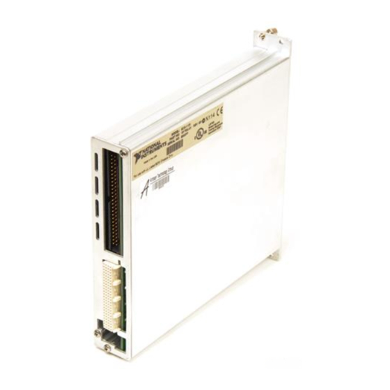
Page 139: Revision A And B Photo And Parts Locator Diagrams
Revision A and B Photo and Parts Locator Diagrams This appendix contains a photograph of the Revision A and B SCXI-1121 signal conditioning module and the general and detailed parts locator diagrams. Figure F-1 shows the SCXI-1121 module. Figures F-2 and F-3 show the general and detailed parts locator diagrams of the Revision A and B SCXI-1121. -
Page 140: Figure F-2. Revision A And B Scxi-1121 General Parts Locator Diagram
Figure F-2. Revision A and B SCXI-1121 General Parts Locator Diagram... -
Page 141: Figure F-3. Revision A And B Scxi-1121 Detailed Parts Locator Diagram
Figure F-3. Revision A and B SCXI-1121 Detailed Parts Locator Diagram... -
Page 142: Technical Support Resources
Technical Support Resources This appendix describes the comprehensive resources available to you in the Technical Support section of the National Instruments Web site and provides technical support telephone numbers for you to use if you have trouble connecting to our Web site or if you do not have internet access. -
Page 143: Germany 089 741 31 30, Greece 30 1 42 96 427, Hong Kong 2645 3186, India
Web sites from If you have trouble connecting to our Web site, please contact your local National Instruments office or the source from which you purchased your National Instruments product(s) to obtain support. For telephone support in the United States, dial 512 795 8248. For... - Page 144 0 enable bit AB2+ positive analog bus 2 line signal AB2– negative analog bus 2 line signal ACH# data acquisition board analog input channel number analog-to-digital © National Instruments Corporation Value –12 –9 – 6 –3 Glossary-1 SCXI-1121 User Manual...
- Page 145 CHSGND chassis ground signal cold-junction reference CLKEN clock enable bit CLKOUTEN scanclock output enable bit CLKSELECT scanclock select bit count bit D*/A data/address line signal digital-to-analog DAQD*/A data acquisition board data/address line signal decibels SCXI-1121 User Manual Glossary-2 www.natinst.com...
- Page 146 EX#– negative excitation output number signal Fahrenheit FIFO first-in-first-out FOUTEN* forced output enable bit forced retransmit bit GBWP gain bandwidth product GUARD guard signal hexadecimal HSCR hardscan control register © National Instruments Corporation Glossary-3 Glossary SCXI-1121 User Manual...
- Page 147 MCH#+ positive analog output channel number signal MCH#– negative analog output channel number signal MISO master-in slave-out signal module number bit MOSI master-out slave-in signal most significant bit SCXI-1121 User Manual Glossary-4 www.natinst.com...
- Page 148 RESET* reset signal root mean square referenced single-ended (input) RSVD reserved bit/signal resistance temperature detector RTEMP read temperature bit referred to input referred to output RTSI real time system integration © National Instruments Corporation Glossary-5 Glossary SCXI-1121 User Manual...
- Page 149 SERDATOUT serial data out signal slot bit SLOT0SEL* slot 0 select signal serial peripheral interface SPICLK serial peripheral interface clock signal slot select signal tempco temperature coefficient TRIG0 trigger 0 signal SCXI-1121 User Manual Glossary-6 www.natinst.com...
- Page 150 Underwriters Laboratory volts positive analog supply signal V– negative analog supply signal volts direct current volts input high volts input low volts output high volts output low volts, root mean square watts © National Instruments Corporation Glossary-7 Glossary SCXI-1121 User Manual...
- Page 151 2-9 gain jumpers, 2-8 jumper W33, 2-6 to 2-7 analog input channels block diagram, 3-9 signal connections, 2-20 to 2-22 © National Instruments Corporation AC-coupled, with high common-mode voltage (figure), 2-21 exceeding input range and common-mode input range (warning), 2-22...
- Page 152 Index cable assemblies. See SCXI-1121 cabling. cables, custom, 1-5 calibration, 3-11 to 3-14 equipment requirements, 3-11 to 3-12 excitation adjust, 3-13 to 3-14 offset null adjust, 3-11 potentiometer reference designators (table), 3-14 CGND signal (table), 2-18, D-3 CH0+ signal (table), 2-19, D-4...
- Page 153 1-5 D*/A signal description (table), 3-4, C-3 SCXIbus equivalents for rear signal connector (table), 3-5 SCXIbus to SCXI-1121 rear signal connector to DAQ board pin equivalences (table), 2-41 DAQD*/A signal. See also communication signals. description (table), 2-38, B-2...
- Page 154 5-55-6 indirect multiplexed scanning, single-module, 5-11 to 5-12 channel scanning from other modules, 5-11 channel scanning from SCXI-1121 via another module, 5-11 to 5-12 initialization of registers, 5-4 input channel jumpers, 2-8 to 2-13 excitation jumpers, 2-9 to 2-13...
- Page 155 2-12 to 2-13 INTR* signal description (table), 3-4, C-3 SCXIbus equivalents for rear signal connector (table), 3-5 SCXIbus to SCXI-1121 rear signal connector to DAQ board pin equivalences (table), 2-41 jumpers fixed jumpers, 2-2 settings for nulling circuits (table), 2-28...
- Page 156 3-18 indirect, 3-18 to 3-19 programming, 5-11 to 5-12 Multiplexed-Output mode, 3-16 MUXCOUNTER, 3-15 to 3-16 National Instruments Web support, G-1 to G-2 NI-DAQ software, 1-2 for Macintosh, 1-3 notation, for programming, 5-1 nulling circuitry, SCXI-1321 terminal block, 2-25 to 2-27...
- Page 157 2-37 to 2-46 analog output, 2-39 communication signals, 2-42 to 2-46 digital I/O, 2-40 to 2-41 pin assignments (figure), 2-37, B-1 SCXIbus to SCXI-1121 to DAQ board pin equivalences (table), 2-41 signal descriptions (table), 2-38, B-2 timing requirements and communication protocol, 2-42...
- Page 158 3-19 multiplexed scanning, 3-17 to 3-18 single-module multiplexed scanning, 3-18 to 3-19 single-module parallel scanning, 3-17 SCXI-1121. See also configuration; installation; theory of operation. block diagram, 3-1 custom cables, 1-5 kit contents, 1-2 major components, 3-2 optional equipment (table), 1-4...
- Page 159 SCXI-1328 terminal block. See SCXI-1320 and SCXI-1328 terminal blocks. SCXI-1340 cable assembly description, E-1 to E-2 installation, E-3 to E-4 SCXI-1121 and MIO-16 pinout equivalences (table), E-2 to E-3 SCXI-1341 Lab-NB, Lab-PC, or Lab-PC+ cable assembly, E-4 to E-6 description, E-4 to E-6...
- Page 160 Index SERCLK signal. See also communication signals. description (table), 2-38, B-2 register writes, 5-2 to 5-3 SCXIbus to SCXI-1121 rear signal connector to DAQ board pin equivalences (table), 2-41 timing requirements (figure), 2-44 SERDATIN signal. See also communication signals. description (table), 2-38, B-2...
- Page 161 SCXIbus to SCXI-1121 rear signal connector to DAQ board pin equivalences (table), 2-41 Slot-Select Register description, 4-6 register writes, 5-2 to 5-4 software, optional, 1-2 to 1-3 software-related resources, G-2 specifications analog input, A-1 to A-2 cold-junction sensor, A-3 to A-4...
- Page 162 Index Web support from National Instruments, G-1 to G-2 online problem-solving and diagnostic resources, G-1 software-related resources, G-2 Worldwide technical support, G-2 Wxx jumpers. See jumpers. SCXI-1121 User Manual Index-12 www.natinst.com...
Need help?
Do you have a question about the SCXI-1121 and is the answer not in the manual?
Questions and answers