Harman Kardon AVR146 Service Manual
5 x 30w 5.1 channel a/v receiver
Hide thumbs
Also See for AVR146:
- Settings manual (3 pages) ,
- Product view (1 page) ,
- Owner's manual (60 pages)
Table of Contents
Advertisement
harman/kardon
5 X 30W 5.1 CHANNEL A/V RECEIVER
ESD WARNING.....................................2
LEAKAGE TESTING...............................3
BASIC SPECIFICATIONS.......................4
PACKAGING........................................5
FRONT PANEL CONTROLS.....................6
REAR PANEL CONNECTIONS................8
REMOTE CONTROL FUNCTIONS..........10
CONNECTIONS/INSTALLATION.............13
OPERATION.......................................23
TROUBLESHOOTING GUIDE.................29
REMOTE & PROCESSOR RESETS..........30
Released 2007
Discontinued XXXX
AVR146
SERVICE MANUAL
CONTENTS
harman/kardon, Inc.
250 Crossways Park Dr.
Woodbury, New York 11797
DISASSEMBLY......................................31
UNIT EXPLODED VIEW..........................35
EXPLODED VIEW PARTS LIST...............36
AMP BIAS ADJUSTMENT......................37
BLOCK DIAGRAM................................38
PCB DRAWINGS.................................39
ELECTRICAL PARTS LIST.....................48
SEMICONDUCTOR PINOUTS................78
SCHEMATICS.....................................164
WIRING DIAGRAM..............................172
Rev0 6/2007
Advertisement
Table of Contents

Related Manuals for Harman Kardon AVR146


Summary of Contents for Harman Kardon AVR146
-
Page 1: Table Of Contents
AVR146 5 X 30W 5.1 CHANNEL A/V RECEIVER SERVICE MANUAL CONTENTS ESD WARNING……………………………….2 DISASSEMBLY…...…………………………..31 LEAKAGE TESTING……………….…..…..3 UNIT EXPLODED VIEW…………..…….…..35 BASIC SPECIFICATIONS…………………..4 EXPLODED VIEW PARTS LIST……………36 PACKAGING…………………………….……5 AMP BIAS ADJUSTMENT……………….…37 FRONT PANEL CONTROLS………..…..…..6 BLOCK DIAGRAM…………………………..38 REAR PANEL CONNECTIONS………….…8 PCB DRAWINGS……………………………39 REMOTE CONTROL FUNCTIONS……….10... -
Page 2: Esd Warning
AVR146 Some semiconductor (solid state) devices can be damaged easily by static electricity. Such components commonly are called Electrostatically Sensitive (ES) Devices. Examples of typical ES devices are integrated circuits and some field effect transistors and semiconductor "chip" components. -
Page 3: Leakage Testing
AVR146 SAFETY PRECAUTIONS The following check should be performed for the continued protection of the customer and service technician. LEAKAGE CURRENT CHECK Measure leakage current to a known earth ground (water pipe, conduit, etc.) by connecting a leakage current tester... -
Page 4: Basic Specifications
All features and specifications are subject to change without notice. Transient Intermodulation Distortion (TIM) Unmeasurable Harman Kardon and Logic 7 are trademarks of Harman International Industries, Incorporated, registered in the United States and/or other countries. Designed to Entertain and are trademarks of Harman International Slew Rate 40V/µsec... -
Page 5: Packaging
AVR146 1. Instruction manual ass'y - Accessories 2. Package Drawing MANUAL ASS'Y CARD WARRANTY POLY BAG AM LOOP ANTENNA ASS'Y SNOW PAD (L) SNOW PAD (R) FM 1 POLE ANT(UL) MANUAL INSTRUCTION BATTERY ASS'Y AVR146 REMOCON BOX ,OUT CARTON TRANSMITTER ASS'Y... -
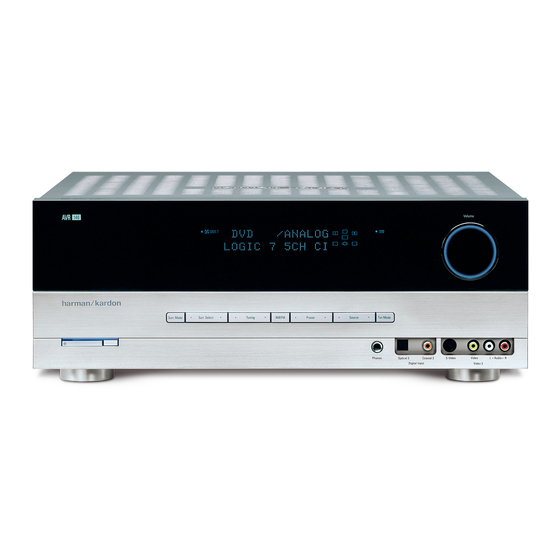
Page 6: Front Panel Controls
AVR146 FRONT-PANEL CONTROLS Main Power Switch: Tuning: This mechanical switch turns the power supply Press either side of this button to tune a radio station. on or off. It is usually left pressed in (On position), and cannot be turned... - Page 7 AVR146 Source Message Display Indicators Surround Mode Speaker/Channel Volume Indicators Input Indicators Power Surround Tuning Preset Stations Headphone Digital Video 3 Jack Audio Inputs Indicator Mode Analog Audio (Optical 3 and Main Power Inputs Tuner Band Source Standby/On Surround...
-
Page 8: Rear Panel Connections
REAR-PANEL CONNECTIONS AM and FM Antenna Terminals: The Bridge/DMP Input: Connect the included AM and Connect the optional Harman Kardon Bridge FM antennas to their respective terminals for radio reception. to this input for use with your iPod (not included). Make... - Page 9 AVR146 Video 1 Video Component Video 2 HDMI HDMI Monitor Video Monitor Input 1 Input 2 FM Antenna Inputs Inputs Outputs Outputs Video 1 DVD A/V HDMI Component Video The Bridge/ Outputs Inputs AM Antenna Inputs (1 & 2)
-
Page 10: Remote Control Functions
AVR146 REMOTE CONTROL FUNCTIONS The AVR 146 remote is capable of controlling up to ten devices, including IR Transmitter Lens: As buttons are pressed on the remote, the AVR itself and an iPod docked in the optional The Bridge accessory. - Page 11 AVR146 IR Transmitter Lens Power On Mute Program Indicator Power Off Input Selectors AVR Selector 6-Channel Input Selector AM/FM Test Tone TV/Video Sleep Volume Controls DSP Surround Not Used On-Screen Display Speaker Setup Channel Level Navigation Digital Input Delay...
- Page 12 AVR146 REMOTE CONTROL FUNCTIONS Speaker Setup: press of a button will cycle to the next available variant of that mode. Press this button to configure speaker sizes, that is, Not all modes or mode groups are available with all sources.
-
Page 13: Connections/Installation
AVR146 CONNECTIONS There are different types of audio and video connections used to Bare wire cables are installed as follows (see Figure 2): connect the receiver to the speakers and video display, and to connect 1. Unscrew the terminal cap until the pass-through hole in the collar the source devices to the receiver. -
Page 14: Audio Connections
Figure 7 – Multichannel Analog Audio Coaxial digital audio jacks are usually color-coded in orange. Although Harman Kardon receivers also include a proprietary, dedicated audio they look similar to analog jacks, they should not be confused, and you connection called “The Bridge/DMP”. If you own an iPod with a dock... - Page 15 AVR146 CONNECTIONS AVR 146 processing any of the data. Although this enables the AVR 146 to be compatible with virtually any HDMI-capable source device and video Component display, it requires a separate audio connection for each source since video cable the AVR 146 doesn’t have access to the audio data in the HDMI stream.
- Page 16 AVR146 INSTALLATION You are now ready to connect your various components to your receiver. Step Three – Connect the Antennas Before beginning, make sure that all components, including the AVR 146, Connect the FM and AM antennas to their terminals. See Figure 18.
- Page 17 AVR146 INSTALLATION We recommend connecting your various sources using the connections NOTE: It’s possible for a source to use none of the connections shown in Table 2 below in order to simplify programming your receiver named for that source. For example, you might connect your and remote control.
- Page 18 AVR146 INSTALLATION inputs. Do not connect any video output on the television set Video 1 Source to any video input on the receiver. See Step Five for information Since this source includes audio and video recording output jacks, it is on connecting the receiver’s video monitor outputs to the...
- Page 19 Interface) input, you may use an HDMI-to-DVI adapter (not included). Bridge With Harman Kardon’s optional The Bridge, you can play audio, video Figure 24 – HDMI and Coaxial 2 Inputs or still images stored on your iPod (not included), use your AVR 146 remote control to operate the iPod, and even charge the iPod while it’s...
- Page 20 The AVR 146’s remote is factory-programmed to control an iPod press the ridged depression and slide the cover towards the top of docked in The Bridge and many Harman Kardon DVD and CD players. the remote. If you have other source devices in your system, follow these steps to...
- Page 21 Alternatively, want to program into the HDMI 2 mode, i.e., DVD, VCR/PVR or you may wish to consider purchasing Harman Kardon’s optional TC 30 CBL/SAT. Then follow the directions in Step 4, below.
- Page 22 AVR146 INSTALLATION Step Nine – Turn On the AVR 146 Two steps are required the first time you turn on the AVR 146. 1. Gently press the Master Power Switch until the word OFF is no longer visible. The Power Indicator above the two power switches should light up in amber, indicating that the AVR is in Standby mode and is ready to be turned on.
-
Page 23: Operation
AVR146 OPERATION Now that you have installed your system components and completed To turn the receiver off, press either the Standby/On Switch on the at least a basic configuration of your receiver, you are ready to begin front panel, or press the AVR Button and the OFF Button on the remote. -
Page 24: Mute Function
AVR146 OPERATION The AVR 146 is designed to reproduce audio with a minimum amount NOTE: The AVR 146 does not have a conventional balance of distortion, which may lead you to think that your hearing and the control. The speaker output level calibration process compen- equipment can handle higher volumes. -
Page 25: Channel Direct Inputs
AVR146 OPERATION The source name will appear in the upper line of the front-panel display. If no signal is present at the component video input, then the S-video or If you retitled the source, only the new title will appear. Otherwise, the composite video input for the source will be selected. -
Page 26: Using The Tuner
AVR146 OPERATION Example 2: In this example, your multichannel disc player is equipped with an HDMI output. Connect it as follows: a) Connect the player’s coaxial digital audio output to the Coaxial 2 input on the AVR. This input is assigned by default to the HDMI 1 source. - Page 27 AVR146 OPERATION Recording Table 4 – Using The Bridge iPod Function Remote Control Key Front-Panel Button Two-channel analog and digital audio signals, as well as composite Play Play ( › Tuner Mode and S-video signals, are normally available at the appropriate recording...
-
Page 28: Selecting A Surround Mode
AVR146 OPERATION Selecting a Surround Mode Surround mode selection can be as simple or sophisticated as your individual system and tastes. Feel free to experiment with the many available surround modes on the AVR 146, and you may find a few that become your favorites for certain sources or program types. -
Page 29: Troubleshooting Guide
• Amplifier is in protection mode • Contact your local Harman Kardon service center due to internal problems No sound from surround or • Incorrect surround mode • Select a mode other than Stereo center speakers •... -
Page 30: Remote & Processor Resets
Surround Mode Button for at least 5 seconds until the RESET message appears in the display. If the receiver still does not function correctly after a processor reset, contact an authorized Harman Kardon service center for assistance. Service centers may be located by visiting our Web site at www.harmankardon.com. -
Page 31: Disassembly
AVR146 DISASSEMBLY AVR146 1. Removing the Top Cabinet 3. Removing the Rear Panel Remove the Screws Remove the Screws 16 17 18 14 15 21 22 4. Removing the Main PCB Remove the Screws 2. Removing the Front Panel... - Page 32 AVR146 AVR146 DISASSEMBLY PROCEDURE TOP-CABINET (21) REMOVAL 1. Remove 13 screws (S1,S7) and then remove the Top-cabinet. FRONT PANEL ASS’Y REMOVAL 1. Remove the Top-cabinet, referring to the previous step1. 2. Disconnect card cable between connector (CN72-17P) on Fip PCB (37-1) and connector (CN72) on Input PCB (39-1).
- Page 33 AVR146 TUNER MODULE (42) REMOVAL 1. Remove the Top-cabinet, referring to the previous step1. 2. Disconnect the card cable between connector (CON1-13P) on the Tuner module (42) and connector (CN13) on the Input PCB (39-1). 3. Remove 2 screws (S8) and then remove the Tuner Module (42).
- Page 34 AVR146 12. Disconnect the card cable between connector (CN72) on the Input PCB (39-1) and connector (CN72-17p) on the Fip PCB (37-1) 13. Remove 11 screws (S8,S15) and then remove the Input PCB (39-1). 12 POWER TRANS (36) & POWER PCB ASS’Y (40) REMOVAL 1.
-
Page 35: Unit Exploded View
AVR146 AVR146 EXPLODED VIEW 39-2 40-3 40-4 40-1 40-5 39-1 40-2 38-2 38-1 40-2 DESCRIPTION PARTS NO. Q,ty Weright ORNAMENT,VOLUME CGU1A318Z CAP,VOLUME CGX1A338MBC63 HOLDER,VOLUME CMH1A214 INDICATOR,VOLUME CGL1A222 WINDOW ASS'Y CGUAVR146 WINDOW,FIP CGU2A399Y BADGE,MODEL CGB1A177Z SHEET,VOLUME CMZ2A090 FILTER,FIP CMZ1A088 BDAGE,HARMAN/KARDON... -
Page 36: Exploded View Parts List
AVR146... -
Page 37: Amp Bias Adjustment
AVR146 AMPLIFIER SECTION BIAS ADJUSTMENT Measurement condition .No input signal or volume position is minimum. Standard value .Ideal current = 48mA (± 5%) .Ideal DC Voltage = 25.92mV (± 5%) DC EVM CUP11911* (MAIN PCB) CN61 CN64 CN63 CN65... - Page 38 AVR146...
-
Page 39: Pcb Drawings
AVR146 harman/kardon AVR146... - Page 40 AVR146...
- Page 41 AVR146...
- Page 42 AVR146...
- Page 43 AVR146...
- Page 44 AVR146...
- Page 45 AVR146...
- Page 46 AVR146...
- Page 47 AVR146...
-
Page 48: Electrical Parts List
AVR146 AVR146 Electrical Parts List Ref. Designator Part Number Description FRONT PCB ASSY CUP11910-1 Capacitors C714 HCBS1H151KBT CAP , CERAMIC 150UF 50V K C716 CCEA1AH331T CAP , ELECT 330UF 10V C723 HCBS1H104ZFT CAP , CERAMIC 0.1UF 50V Z C728... - Page 49 AVR146 Ref. Designator Part Number Description FRONT PCB ASSY CUP11910-1 Miscellaneous L702 HLQ02C100KT COIL , AXAIL 10uH BK71 CMD1A209 BRACKET , FLT A4-92-1739 BK72 CMD1A209 BRACKET , FLT A4-92-1739 BK73 CMD1A209 BRACKET , FLT A4-92-1739 BN81 CWB2C908200BM WIRE ASS'Y...
- Page 50 AVR146 Ref. Designator Part Number Description PCB , FRONT PANEL KEY CUP11910-2 Miscellaneous S702 HST1A020ZT SW , TACT 1A020 S703 HST1A020ZT SW , TACT 1A020 S704 HST1A020ZT SW , TACT 1A020 S705 HST1A020ZT SW , TACT 1A020 S706 HST1A020ZT...
- Page 51 AVR146 Ref. Designator Part Number Description PCB , VR JACK CUP11910-6 BN10 CWZAVR230BN10 WIRE ASS'Y (SHIELD) WIRE BN41 CWZAVR130BN41 WIRE ASS'Y (SHIELD) WIRE JK85 CJJ9M003Z JACK , S-VIDEO S-VIDEO JACK JK86 CJJ4S023Y JACK , BOARD BOARD JACK JW84 CWE8202110RV...
- Page 52 AVR146 Ref. Designator Part Number Description PCB , PHONE JACK CUP11910-5 R911 CRD20TJ221T RES , CARBON 220 OHM 1/5W J R912 CRD20TJ221T RES , CARBON 220 OHM 1/5W J R913 CRD20TJ102T RES , CARBON 1K OHM 1/5W J R915...
- Page 53 AVR146 Ref. Designator Part Number Description MAIN PCB/HEATSINK (CUP11911Z) C685 CCEA1HH100T CAP , ELECT 10UF 50V C726 CCKT1H221KB CAP , CERAMIC 220PF 50V C900 HCQI1H473JZT CAP , MYLAR 0.047UF 50V C901 HCQI1H473JZT CAP , MYLAR 0.047UF 50V C905 CCFT1H223ZF CAP , CERAMIC 0.022UP 50V...
- Page 54 AVR146 Ref. Designator Part Number Description MAIN PCB/HEATSINK (CUP11911Z) D911 CVD1SS133MT DIODE 1SS133 D912 CVD1SS133MT DIODE 1SS133 D914 CVD1SS133MT DIODE 1SS133 D917 CVD1SS133MT DIODE 1SS133 D953 CVD1SS133MT DIODE 1SS133 D954 CVD1N4003SRT RECT , DIODE 1N4003 D955 CVD1N4003SRT RECT , DIODE...
- Page 55 AVR146 Ref. Designator Part Number Description MAIN PCB/HEATSINK (CUP11911Z) Q951 HVTKRC107MT TRANSISTOR NPN KRC107M Q952 HVTKRA107MT KRA107M TRANSISTOR PNP Q960 HVTKRC107MT TRANSISTOR NPN KRC107M Q961 HVTKTA1024YT KTA1024YT TRANSISTOR PNP Q991 HVTKRC107MT TRANSISTOR NPN KRC107M Q992 HVTKRA107MT TRANSISTOR PNP KRA107M...
- Page 56 AVR146 Ref. Designator Part Number Description MAIN PCB/HEATSINK (CUP11911Z) R556 CRD20TJ273T RES , CARBON 27K OHM 1/5W J R557 CRD20TJ273T RES , CARBON 27K OHM 1/5W J R558 CRD20TJ273T RES , CARBON 27K OHM 1/5W J R559 CRD20TJ273T RES , CARBON...
- Page 57 AVR146 Ref. Designator Part Number Description MAIN PCB/HEATSINK (CUP11911Z) R637 CRD25FJ180T RES , CARBON 18 OHM 1/4W J R638 CRD25FJ180T RES , CARBON 18 OHM 1/4W J R639 CRD25FJ180T RES , CARBON 18 OHM 1/4W J R640 CRD25FJ180T RES , CARBON...
- Page 58 AVR146 Ref. Designator Part Number Description MAIN PCB/HEATSINK (CUP11911Z) R910 CRD20TJ105T RES , CARBON 1M OHM 1/5W J R911 CRD25TJ680T RES , CARBON 68 OHM 1/4W J R912 CRD20TJ332T RES , CARBON 3.3K OHM 1/5W J R917 CRD25TJ393T RES , CARBON...
- Page 59 AVR146 Ref. Designator Part Number Description MAIN PCB/HEATSINK (CUP11911Z) CN62 CJP02GA01ZY WAFER, STRAIGHT, 2PIN WAFER CN63 CJP02GA01ZY WAFER, STRAIGHT, 2PIN WAFER CN64 CJP02GA01ZY WAFER, STRAIGHT, 2PIN WAFER CN65 CJP02GA01ZY WAFER, STRAIGHT, 2PIN WAFER CN91 CJP02GA89ZY WAFER WAFER CN92 KJP02KA060ZY...
- Page 60 AVR146 Ref. Designator Part Number Description PCB , POWER TRANS CUP11916-3,4 C121 HCBS1H103ZFT CAP , CERAMIC 0.01UF 50V C123 CCFT1H473ZF CAP , CERAMIC 0.047UF 50V ZF C125 CCFT1H473ZF CAP , CERAMIC 0.047UF 50V ZF C126 CCFT1H473ZF CAP , CERAMIC 0.047UF 50V ZF...
- Page 61 AVR146 Ref. Designator Part Number Description PCB , POWER TRANS CUP11916-3,4 R917 CRD20TJ153T RES , CARBON 15K OHM 1/5W J R918 CRD20TJ153T RES , CARBON 15K OHM 1/5W J R919 CRD20TJ153T RES , CARBON 15K OHM 1/5W J R920...
- Page 62 AVR146 Ref. Designator Part Number Description PCB , BIAS TR CUP11916-2 JK78 CJJ4S022Z JACK , BOARD JACK C851 CCEA1HH100T CAP , ELECT 10UF 50V C852 CCEA1HH100T CAP , ELECT 10UF 50V C853 CCEA1HH100T CAP , ELECT 10UF 50V C854...
- Page 63 AVR146 Ref. Designator Part Number Description PCB , REGULATOR CUP11916-5,6 IC90 HVIL7815CP I.C, REGULATOR(+15V) IC91 HVIL7915CP I.C, REGULATOR(-15V) IC93 HVIL7905CP I.C, REGULATOR(-5V) IC94 HVIL7805CP I.C, REGULATOR(+5V) IC95 HVINJM7812FA I.C , REGULATOR(+12V) PCB , INPUT CUP11912-1 Capacitors C201 CCUS1H221JA CAP , CHIP...
- Page 64 AVR146 Ref. Designator Part Number Description PCB , INPUT CUP11912-1 C326 CCUS1H561JA CAP , CHIP 560PF C327 CCUS1H561JA CAP , CHIP 560PF C328 CCUS1H561JA CAP , CHIP 560PF C329 CCUS1H561JA CAP , CHIP 560PF C330 CCUS1H561JA CAP , CHIP...
- Page 65 AVR146 Ref. Designator Part Number Description PCB , INPUT CUP11912-1 C727 CCUS1H104KC CAP , CHIP 0.1UF C729 CCUS1H104KC CAP , CHIP 0.1UF C731 CCUS1H104KC CAP , CHIP 0.1UF C733 CCUS1H104KC CAP , CHIP 0.1UF C734 CCUS1H102KC CAP , CHIP...
- Page 66 AVR146 Ref. Designator Part Number Description PCB , INPUT CUP11912-1 C371 CCEA1HH100T CAP , ELECT 10UF 50V C372 CCEA1HH100T CAP , ELECT 10UF 50V C373 CCEA1HH100T CAP , ELECT 10UF 50V C374 CCEA1HH100T CAP , ELECT 10UF 50V C375...
- Page 67 AVR146 Ref. Designator Part Number Description PCB , INPUT CUP11912-1 IC20 CVINJW1197FC2 IC , SW(WITH VOLUME) IC21 HVINJM2068MDTE1 I.C , DUAL OP AMP IC22 HVINJM2068MDTE1 I.C , DUAL OP AMP IC23 HVINJM2068MDTE1 I.C , DUAL OP AMP IC25 HVINJM2068MDTE1 I.C , DUAL OP AMP...
- Page 68 AVR146 Ref. Designator Part Number Description PCB , INPUT CUP11912-1 RN87 CRJ104DJ330T RES , 4ARRAY (1608*4) 33 OHM/1608*4 RN88 CRJ104DJ103T RES , 4ARRAY (1608*4) 10K OHM/1608*4 RN89 CRJ104DJ103T RES , 4ARRAY (1608*4) 10K OHM/1608*4 RN90 CRJ104DJ330T RES , 4ARRAY (1608*4)
- Page 69 AVR146 Ref. Designator Part Number Description PCB , INPUT CUP11912-1 R273 CRJ10DJ102T RES , CHIP 1K OHM R274 CRJ10DJ102T RES , CHIP 1K OHM R275 CRJ10DJ102T RES , CHIP 1K OHM R276 CRJ10DJ102T RES , CHIP 1K OHM R281...
- Page 70 AVR146 Ref. Designator Part Number Description PCB , INPUT CUP11912-1 R382 CRJ10DJ561T RES , CHIP 560 OHM R383 CRJ10DJ561T RES , CHIP 560 OHM R384 CRJ10DJ561T RES , CHIP 560 OHM R385 CRJ10DJ561T RES , CHIP 560 OHM R386...
- Page 71 AVR146 Ref. Designator Part Number Description PCB , INPUT CUP11912-1 R778 CRJ10DJ103T RES , CHIP 10K OHM R782 CRJ10DJ272T RES , CHIP 2.7K OHM R783 CRJ10DJ272T RES , CHIP 2.7K OHM R784 CRJ10DJ473T RES , CHIP 47K OHM R785...
- Page 72 AVR146 Ref. Designator Part Number Description IPOD PCB(CUP11912-2) C436 CCUS1H120JA CAP, CHIP 12PF C440 CCUS1H223KC CAP , CHIP 0.022UF C445 HCEC1CRV2220T CAP , ELEC (SMD) 22UF/16V Semiconductors D400 CVD1SS355T CHIP , DIODE 1SS355T D401 CVD1SS355T CHIP , DIODE 1SS355T...
- Page 73 AVR146 Ref. Designator Part Number Description PCB , VIDEO CUP11917 C463 CCUS1H223KC CAP , CHIP 0.022UF C466 CCUS1H223KC CAP , CHIP 0.022UF C468 CCUS1H223KC CAP , CHIP 0.022UF C471 CCUS1H223KC CAP , CHIP 0.022UF C473 CCUS1H223KC CAP , CHIP 0.022UF...
- Page 74 AVR146 Ref. Designator Part Number Description PCB , VIDEO CUP11917 C474 CCEA1CH101T CAP , ELECT 100UF 16V C503 CCEA1HH100T CAP , ELECT 10UF 50V C505 CCEA1HH100T CAP , ELECT 10UF 50V C514 CCEA1HH100T CAP , ELECT 10UF 50V C515...
- Page 75 AVR146 Ref. Designator Part Number Description PCB , VIDEO CUP11917 Q551 HVTKTD1304T TRANSISTOR , CHIP (MUTE) NPN KTD1304 Q552 HVTKRA104S TRANSISTOR, CHIP PNP KRA104S Q555 HVTKTD1304T TRANSISTOR , CHIP (MUTE) NPN KTD1304 Q556 HVTKRA104S TRANSISTOR, CHIP PNP KRA104S Q501...
- Page 76 AVR146 Ref. Designator Part Number Description PCB , VIDEO CUP11917 R540 CRJ10DJ101T RES , CHIP 100 OHM R541 CRJ10DJ181T RES , CHIP 180 OHM R542 CRJ10DJ392T RES . CHIP 3.9K OHM R543 CRJ10DJ1R8T RES , CHIP 1.8 OHM R545...
- Page 77 AVR146 Ref. Designator Part Number Description PCB , VIDEO CUP11917 CN43 CJP03GA01ZY WAFER WAFER CN45 CJP07GA117ZY WAFER WAFER JK40 CJJ9P003Z JACK , (S-VIDEO + CVBS) JACK JK41 CJJ9R001Z JACK , (S-VIDEO + CVBS) JACK JK62 CJJ4R045Z JACK , BOARD...
-
Page 78: Semiconductor Pinouts
AVR146... - Page 79 AVR146...
- Page 80 AVR146...
- Page 81 AVR146...
- Page 82 AVR146...
- Page 83 AVR146...
- Page 84 AVR146...
- Page 85 AVR146...
- Page 86 AVR146...
- Page 87 AVR146...
- Page 88 AVR146...
- Page 89 AVR146...
- Page 90 AVR146...
- Page 91 AVR146...
- Page 92 AVR146...
- Page 93 AVR146 Excel Semiconductor inc. ES29LV800E 8Mbit(1M x 8/512K x 16) CMOS 3.0 Volt-only, Boot Sector Flash Memory GENERAL FEATURES • Minimum 100,000 program/erase cycles per sector • 20 Year data retention at 125 • Single power supply operation - 2.7V -3.6V for read, program and erase operations SOFTWARE FEATURES •...
- Page 94 AVR146 Excel Semiconductor inc. GENERAL PRODUCT DESCRIPTION The ES29LV800 is completely compatible with the The ES29LV800 is a 8 megabit, 3.0 volt-only flash JEDEC standard command set of single power sup- memory device, organized as 1M x 8 bits (Byte ply Flash.
-
Page 95: Block Diagram
AVR146 Excel Semiconductor inc. PRODUCT SELECTOR GUIDE Family Part Number ES29LV800 Voltage Range 2.7 ~ 3.6V Speed Option Max Access Time (ns) CE# Access (ns) OE# Access (ns) FUNCTION BLOCK DIAGRAM RY/BY# Timer/ Vcc Detector DQ0-DQ15(A-1) Counter Analog Bias... - Page 96 AVR146 Excel Semiconductor inc. PIN DESCRIPTION Description A0-A18 19 Addresses DQ0-DQ14 15 Data Inputs/Outputs DQ15 (Data Input/Output, Word Mode) DQ15/A-1 A-1 (LSB Address Input, Byte Mode) Chip Enable Output Enable Write Enable RESET# Hardware Reset Pin, Active Low BYTE#...
-
Page 97: Connection Diagram
AVR146 Excel Semiconductor inc. CONNECTION DIAGRAM BYTE# DQ15/A-1 48-Pin Standard TSOP DQ14 DQ13 DQ12 RESET# ES29LV800 DQ11 RY/BY# DQ10 48-Ball FBGA (6 x 8 mm) (Top View, Balls Facing Down) DQ15/ BYTE# DQ14 DQ13 DQ12 RESET# DQ10 DQ11... -
Page 98: Ordering Information
AVR146 HY57V161610E 2 Banks x 512K x 16 Bit Synchronous DRAM DESCRIPTION THE Hynix HY57V161610E is a 16,777,216-bits CMOS Synchronous DRAM, ideally suited for the main memory and graphic appli- cations which require large memory density and high bandwidth. HY57V161610E is organized as 2banks of 524,288x16. - Page 99 AVR146 HY57V161610E PIN CONFIGURATION DQ15 DQ15 DQ14 DQ14 VSSQ VSSQ DQ13 DQ13 DQ12 DQ12 VDDQ VDDQ DQ11 DQ11 DQ10 DQ10 VSSQ VSSQ VDDQ VDDQ 50pin TSOP II 50pin TSOP II VDDQ VDDQ 400mil x 825mil 400mil x 825mil LDQM LDQM 0.8mm pin pitch...
- Page 100 AVR146 HY57V161610E FUNCTIONAL BLOCK DIAGRAM 1Mx16 Synchronous DRAM Self Refresh Counter Refresh Refresh Interval Timer Counter 512Kx16 Bank 0 Address[0:10] Sense AMP & I/O gates Column Decoder Address Precharge Register Row Active BA(A11) Column Addr. Column Active Latch & Counter...
- Page 101 AVR146 HY57V161610E COMMAND TRUTH TABLE A10/ Command CKEn-1 CKEn A0~A9 Note Mode Register Set OP code No Operation Bank Active Row Address Read Column Address Read with Auto precharge Write Column Address Write with Auto precharge Precharge All Bank...
- Page 102 AVR146 Philips Semiconductors Product specification Hex inverter 74HCU04 FEATURES • Output capability: standard • I category: SSI GENERAL DESCRIPTION The 74HCU04 is a high-speed Si-gate CMOS device and is pin compatible with low power Schottky TTL (LSTTL). It is specified in compliance with JEDEC standard no. 7A.
- Page 103 AVR146 Philips Semiconductors Product specification Hex inverter 74HCU04 PIN DESCRIPTION PIN NO. SYMBOL NAME AND FUNCTION 1, 3, 5, 9, 11, 13 1A to 6A data inputs 2, 4, 6, 8, 10, 12 1Y to 6Y data outputs ground (0 V) positive supply voltage Fig.1 Pin configuration.
- Page 104 AVR146 74ACT04 HEX INVERTER HIGH SPEED: t = 5.0ns (TYP.) at V = 5V LOW POWER DISSIPATION: = 2µA(MAX.) at T =25°C COMPATIBLE WITH TTL OUTPUTS = 2V (MIN.), V = 0.8V (MAX.) 50Ω TRANSMISSION LINE DRIVING CAPABILITY TSSOP...
- Page 105 AVR146 NJM2595 5-INPUT 3-OUTPUT VIDEO SWITCH GENERAL DESCRIPTION PACKAGE OUTLINE The NJM2595 is a 5-input 3-output video switch. Its switches select one from five signals received from VTR,TV,DVD, TV-GAME and others. The NJM2595 is designed for audio items, such as AV amplifier and others.
- Page 106 AVR146 NJM2595 EQUIVALENT CIRCUIT PIN No. PIN NAME INSIDE EQUIVALENT CIRCUIT VOLTAGE Vin1 Vin2 Vin3 Vin4 Vin5 Vout1 Vout2 Vout3 2.1k Vout...
- Page 107 AVR146 NJM2595 EQUIVALENT CIRCUIT PIN No. PIN NAME INSIDE EQUIVALENT CIRCUIT VOLTAGE TEST CIRCUIT Vout2.2 Vout2.1 Vout3.2 Vout3.1 75 Ω 75 Ω 75 Ω 75 Ω 0.1µF Vin1 Vin2 75 Ω 75 Ω 100µF 10µF 10µF 1 10µF 10µF 10µF...
- Page 108 AVR146...
- Page 109 AVR146...
- Page 110 AVR146...
- Page 111 AVR146...
- Page 112 AVR146...
- Page 113 AVR146...
- Page 114 AVR146...
- Page 115 AVR146...
- Page 116 AVR146...
- Page 117 AVR146...
- Page 118 AVR146...
- Page 119 AVR146...
- Page 120 AVR146 HCF4053B TRIPLE 2-CHANNEL ANALOG MULTIPLEXER/DEMULTIPLEXER LOW "ON" RESISTANCE : 125Ω (Typ.) OVER 15V p.p SIGNAL-INPUT RANGE FOR = 15V HIGH "OFF" RESISTANCE : CHANNEL LEAKAGE ± 100pA (Typ.) at V = 18V BINARY ADDRESS DECODING ON CHIP HIGH DEGREE OF LINEARITY : < 0.5% DISTORTION TYP.
- Page 121 AVR146 HCF4053B INPUT EQUIVALENT CIRCUIT PIN DESCRIPTION PIN No SYMBOL NAME AND FUNCTION 11, 10, 9 A, B, C Binary Control Inputs Inhibit Inputs 12, 13, 2, 1, ax,ay,bx,by,cx,cy Input/ IN/OUT 5, 3 Output OUT/IN ax or ay OUT/IN...
- Page 122 AVR146...
- Page 123 AVR146...
- Page 124 AVR146...
- Page 125 AVR146...
- Page 126 AVR146...
- Page 127 AVR146...
- Page 128 AVR146...
- Page 129 AVR146...
- Page 130 AVR146...
- Page 131 AVR146...
- Page 132 AVR146...
- Page 133 AVR146...
- Page 134 AVR146...
- Page 135 AVR146 AK4589 2/8-Channel Audio CODEC with DIR PVSS PVDD X'tal Clock Oscillato r 8 to 3 Recovery Clock MCKO1 Generator Input MCKO2 Selector LRCK2 DAIF A udio BICK2 Decode r SDTO2 DAUX2 A VDD A VSS DVDD Error &...
- Page 136 AVR146 ASAHI KASEI [AK4589] オーダリングガイド -10 ∼ +70°C AK4589VQ 80pin LQFP(0.5mm pitch) 評価ボード AKD4589 ピン配置 TEST1 INT1 BOUT TVDD DVDD AVSS DVSS AVDD VREFH XT I VCOM (Top View) TEST3 MCKO2 MCKO1 ROUT1+ COUT ROUT1- UOUT LOUT1+ VOUT LOUT1-...
- Page 137 AVR146 ASAHI KASEI [AK4589] AK4588 との相違点 Functions AK4588 AK4589 DAC 出力 シングルエンド 差動 DAC S/(N+D) 90dB 94dB DAC S/N 106dB 114dB Typ ±2.7Vpp DAC Output voltage Typ 3.0Vpp DAC AOUT AOUT=0.6xVREFH AOUT=0.54xVREFH Load Resistance 5k ohm 2k ohm ±1.0 Frequency Response 80kHz +0/-0.6...
- Page 138 AVR146 ASAHI KASEI [AK4589] ピン/機能 Pin Name Function INT1 Interrupt 1 Pin Block-Start Output Pin for Receiver Input BOUT “H” during first 40 flames. TVDD Output Buffer Power Supply Pin, 2.7V∼5.25V DVDD Digital Power Supply Pin, 4.75V∼5.25V DVSS Digital Ground Pin...
- Page 139 AVR146 ASAHI KASEI [AK4589] Pin Name Function Power-Down Mode Pin When “L”, the AK4589 is powered-down, all digital output pins go “L”, all registers are reset. When CAD1/0 pins are changed, the AK4589 should be reset by PDN pin.
- Page 140 AVR146 ASAHI KASEI [AK4589] Pin Name Function AVDD Analog Power Supply Pin, 4.75V∼5.25V Analog Ground Pin, 0V AVSS Receiver Channel 0 Pin (Internal biased pin. Internally biased at PVDD/2) No Connect pin No internal bonding. This pin should be connected to PVSS.
- Page 141 AVR146 ASAHI KASEI [AK4589] 使用しないピンの処理について 使用しない入出力ピンは下記の設定を行い、適切に処理して下さい。 Classification Pin Name Setting Analog RX0-7, LOUT1-4, ROUT1-4, LIN, RIN These pins should be open. INT0-1, BOUT, XTO, MCKO1-2, COUT, UOUT, These pins should be open. VOUT, SDTO1-2, CDTO, DZF1-2, TX1-0 Digital These pins should be connected to DVSS.
- Page 142 AVR146 Video Switch · 75Ω driver · Y/C mix MM1501 MITSUMI Video Switch · 75Ω driver · Y/C mix Monolithic IC MM1501 Series Outline This IC extends the series of ICs for video/audio signal switching, with a 2-input 1-output single video switch, video signal/chroma signal 75Ω...
-
Page 143: Block Diagram
AVR146 Video Switch · 75Ω driver · Y/C mix MM1501 MITSUMI Block Diagram MM1501 MM1502 MM1503 MM1504 MM1505 MM1506... - Page 144 AVR146 Video Switch · 75Ω driver · Y/C mix MM1501 MITSUMI MM1507 MM1508 MM1509 MM1510 MM1511 MM1512...
- Page 145 AVR146...
- Page 146 AVR146...
- Page 147 AVR146...
- Page 148 AVR146 M24C64 M24C32 64Kbit and 32Kbit Serial I²C Bus EEPROM FEATURES SUMMARY Two-Wire I C Serial Interface Figure 1. Packages Supports 400kHz Protocol Single Supply Voltage: – 4.5 to 5.5V for M24Cxx – 2.5 to 5.5V for M24Cxx-W –...
- Page 149 AVR146 M24C64, M24C32 SUMMARY DESCRIPTION These I C-compatible electrically erasable pro- Table 2. Signal Names grammable memory (EEPROM) devices are orga- E0, E1, E2 Chip Enable nized as 8192 x 8 bits (M24C64) and 4096 x 8 bits (M24C32).
- Page 150 AVR146 M24C64, M24C32 SIGNAL DESCRIPTION Serial Clock (SCL). This input signal is used to rial Data (SDA) to V (Figure 4. indicates how strobe all data in and out of the device. In applica- the value of the pull-up resistor can be calculated).
- Page 151 AVR146 M24C64, M24C32 MEMORY ORGANIZATION The memory is organized as shown in Figure Figure 6. Block Diagram High Voltage Control Logic Generator I/O Shift Register Address Register Data and Counter Register 1 Page X Decoder AI06899 7/26...
- Page 152 AVR146 M24C64, M24C32 DEVICE OPERATION The device supports the I C protocol. This is sum- Data (SDA) Low to acknowledge the receipt of the marized in Figure 5.. Any device that sends data eight data bits. on to the bus is defined to be a transmitter, and Data Input any device that reads the data to be a receiver.
- Page 153 AVR146 M24C64, M24C32 Figure 7. Write Mode Sequences with WC=1 (data write inhibited) NO ACK BYTE WRITE DEV SEL BYTE ADDR BYTE ADDR DATA IN NO ACK PAGE WRITE DEV SEL BYTE ADDR BYTE ADDR DATA IN 1 DATA IN 2...
- Page 154 AVR146 M24C64, M24C32 Page Write The bus master sends from 1 to 32 bytes of data, each of which is acknowledged by the device if The Page Write mode allows up to 32 bytes to be Write Control (WC) is Low. If Write Control (WC) is...
- Page 155 AVR146 M24C64, M24C32 Figure 9. Write Cycle Polling Flowchart using ACK WRITE Cycle in Progress START Condition DEVICE SELECT with RW = 0 Returned First byte of instruction with RW = 0 already decoded by the device Next Operation is...
- Page 156 AVR146 M24C64, M24C32 Figure 10. Read Mode Sequences NO ACK CURRENT ADDRESS DEV SEL DATA OUT READ NO ACK RANDOM ADDRESS DEV SEL * BYTE ADDR BYTE ADDR DEV SEL * DATA OUT READ NO ACK SEQUENTIAL CURRENT DEV SEL...
- Page 157 AVR146 LOW VOL TAGE DETECTOR × 5VT SERIES × PIN CONFIGURATION TO-92 • SOT-89 SOT-23-5 • • (mark side) (mark side) (mark side) PIN DESCRIPTION TO-92 SOT-89 SOT-23-5 • • • Pin No. Symbol Pin No. Symbol Pin No.
- Page 158 AVR146 VOL TAGE DETECTOR × 5VL SERIES × PIN CONFIGURATION TO-92 SOT-89 SOT-23-5 • • • (mark side) (mark side) (mark side) PIN DESCRIPTION TO-92 SOT-89 SOT-23-5 • • • Pin No Symbol Pin No Symbol Pin No Symbol...
- Page 159 AVR146 1A LOWDROP OUT VOLTAGE REGULATOR (ADJUSTABLE & FIXED) LM1117 FEATURES SOT-223 PKG (FRONT VIEW) ● Output Current up to 1 A ● Low Dropout Voltage ( 700mV at 1A Output Current ) PIN FUNCTION ● Three Terminal Adjustable or Fixed 1.5V, 1.8V, 2.5V, 2.85V, 1.
- Page 160 AVR146 NJM2391 LOW DROPOUT VOLTAGE REGULATOR GENERAL DESCRIPTION PACKAGE OUTLINE The NJM2391 is low dropout voltage regulators featuring high precision voltage. It is suitable for Notebook PCs, PC cards and hard disks where 3.3V need to be generated from 5V supply.
- Page 161 AVR146 TRANSISTOR, REGULATOR IC BLOCK DIAGRAM TO-92L TO-92M TO-92 TO-220 1. Emitter 1. Emitter 1. Emitter 1. GND 2. Collector 2. Collector 2. Collector 2. INPUT 3. Base 3. Base 3. Base 3. OUTPUT 12 3 1 2 3...
- Page 162 AVR146 ULTRA-SMALL PACKAGE HIGH-PRECISION VOLTAGE DETECTOR Rev.3.2 S-808xxC Series Pin Configurations Table 7 SC-82AB Top view Pin No. Pin name Pin description Voltage detection output pin Voltage input pin No connection GND pin *1. The NC pin is electrically open.
-
Page 163: Absolute Maximum Ratings
AVR146 ULTRA-SMALL PACKAGE HIGH-PRECISION VOLTAGE DETECTOR Rev.3.2 S-808xxC Series S-80842CNY Table 11 TO-92 Bottom view Pin No. Pin name Pin description Voltage detection output pin Voltage input pin GND pin Figure 8 Absolute Maximum Ratings 1. Detection Voltage Typ. 1.4 V or Less Products Table 12 (Ta = 25 °... -
Page 164: Schematics
AVR146... - Page 165 AVR146...
- Page 166 AVR146...
- Page 167 AVR146...
- Page 168 AVR146...
- Page 169 AVR146...
- Page 170 AVR146...
- Page 171 AVR146...
-
Page 172: Wiring Diagram
AVR146...
Need help?
Do you have a question about the AVR146 and is the answer not in the manual?
Questions and answers