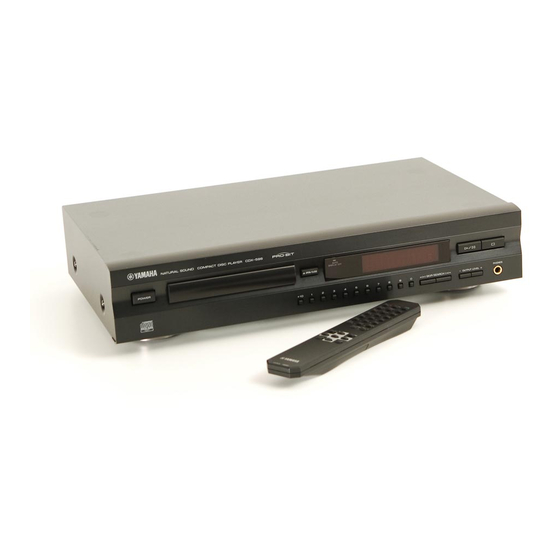
Yamaha CDX-596 Service Manual
Hide thumbs
Also See for CDX-596:
- Owner's manual (28 pages) ,
- Product catalog (44 pages) ,
- Owner's manual (164 pages)
Table of Contents
Advertisement
TEXT/
This manual has been provided for the use of authorized YAMAHA Retailers and their service personnel.
It has been assumed that basic service procedures inherant to the industry, and more specifically YAMAHA Products, are already
known and understood by the users, and have therefore not been restated.
WARNING:
-
+
OUTPUT LEVEL
IMPORTANT:
The data provided is believed to be accurate and applicable to the unit(s) indicated on the cover. The research, engineering, and
service departments of YAMAHA are continually striving to improve YAMAHA products. Modifications are, therefore, inevitable
and specifications are subject to change without notice or obligation to retrofit. Should any discrepancy appear to exist, please contact
the distributor's Service Division.
WARNING:
IMPORTANT:
4
0
0
CONTENTS
TO SERVICE PERSONNEL ....................................... 1-2
REAR PANELS .............................................................. 3
SPECIFICATIONS .......................................................... 4
INTERNAL VIEW ........................................................... 4
DISASSEMBLY PROCEDURES ................................ 5,6
STANDARD OPERATION CHART ............................ 6,7
TEST MODE ................................................................ 7,8
ERROR MESSAGE ................................................... 9,10
DISPLAY DATA ........................................................... 11
1 0 0 7 0 8
COMPACT DISC PLAYER
CDX-596
SERVICE MANUAL
SERVICE MANUAL
SERVICE MANUAL
IMPORTANT NOTICE
Failure to follow appropriate service and safety procedures when servicing this product may result in personal
injury, destruction of expensive components and failure of the product to perform as specified. For these reasons,
we advise all YAMAHA product owners that all service required should be performed by an authorized
YAMAHA Retailer or the appointed service representative.
The presentation or sale of this manual to any individual or firm does not constitute authorization, certification or
recognition of any applicable technical capabilities, or establish a principle-agent relationship of any form.
Static discharges can destroy expensive components. Discharge any static electricity your body may have accumu-
lated by grounding yourself to the ground buss in the unit (heavy gauge black wires connect to this buss).
Turn the unit OFF during disassembly and parts replacement. Recheck all work before you apply power to the unit.
IC DATA .................................................................. 12-16
BLOCK DIAGRAM ....................................................... 17
PRINTED CIRCUIT BOARD ................................... 18-21
IC BLOCK .................................................................... 22
WAVEFORMS .............................................................. 23
SCHEMATIC DIAGRAM .............................................. 24
PARTS LIST ............................................................ 25-33
REMOTE CONTROL TRANSMITTER ......................... 34
CDX-596
Advertisement
Table of Contents

Related Manuals for Yamaha CDX-596


Summary of Contents for Yamaha CDX-596
-
Page 1: Table Of Contents
This manual has been provided for the use of authorized YAMAHA Retailers and their service personnel. It has been assumed that basic service procedures inherant to the industry, and more specifically YAMAHA Products, are already known and understood by the users, and have therefore not been restated. -
Page 2: To Service Personnel
CDX-596 TO SERVICE PERSONNEL 1. Critical Components Information. Components having special characteristics are marked and must be replaced with parts having specifications equal to those originally installed. Meter impedance should be equivalent to 1500 ohm shunted by 0.15µF. Leakage current must not exceed 0.5mA. - Page 3 CDX-596 G, B models CLASS 1 LASER PRODUCT G, B models English THIS PRINTING (SEE POSITION SHOWN IN THE ILLUSTRATION) INFORMS THE USER THAT THE APPARATUS CONTAINS A LASER COMPONENT. THIS LABEL (SEE POSITION SHOWN IN THE ILLUSTRATION) WARNS THAT ANY FURTHER PROCEDURE WILL BRING THE USER INTO EXPOSURE WITH THE LASER BEAM.
-
Page 4: Rear Panels
CDX-596 REAR PANELS A model G, B models... -
Page 5: Specifications
CDX-596 SPECIFICATIONS DIMENSION Output Level 1kHz, 0dB 2.0 ± 0.5Vrms Signal to Noise Ratio (EIAJ) 115dB Dynamic Range 100dB Harmonic Distortion+Noise (1kHz) 0.0025% Frequency Response 2Hz — 20kHz ±0.5dB Power Requirements B, G models 230V AC 50Hz A model 240V AC 50Hz... -
Page 6: Disassembly Procedures
CDX-596 DISASSEMBLY PROCEDURES (Remove parts in disassembly order as numbered.) 1. Removal of Top Cover Top Cover a. Remove 4 screws ( ) and 3 screws ( ) in Fig. 1. b. Lift the Top Cover at the rear and move it rear-ward. -
Page 7: Standard Operation Chart
CDX-596 Pick-up Head Gear A Check that the disc table height is as specified below. Disc Table Sled Shaft 19.4 ± 0.2mm Fig. 5 Stopper STANDARD OPERATION CHART POWER ON If a disc is not loaded, "0:00" appears in the time indicator. -
Page 8: Test Mode
CDX-596 Tracking gain rough ADJ Tracking balance ADJ (only tray OPEN/CLOSE) Focus balance ADJ Focus gain ADJ Tracking gain ADJ * TOC READ - * Data f etch cycle - TRACK NO. “1” is searched. After searching the beginning, PLAY starts. - Page 9 CDX-596 (2) Shown below are the panel key and remote control transmitter functions in the TEST mode. Function List of Panel keys Note) "Traverse servo" means the same as "feed servo". PANEL KEY FUNCTION OPEN/CLOSE Tray open/close. FOON, TRON, SPON, TVON(FEON).
-
Page 10: Error Message
CDX-596 ERROR MESSAGE (1) When operation is terminated in an abnormal condition (stop or open), pressing STOP on the remote control while pressing STOP on the panel will set to the error message display enable mode. (2) Shown below is an example of display. ("E-73" as an example) (3) This function stays effective till the power is turned OFF. - Page 11 CDX-596 c) Operates as if no disc loaded. (although loaded) 2) Troubleshooting from System Malfunctions a) Tray fails to come out/go in. Does tray Poor tray loading. load properly? Poor mechanism Tray starts to operation. move but stops. Wire caught.
-
Page 12: Display Data
CDX-596 DISPLAY DATA V300 : 14-BT-56GN &0 PATTERN AREA PIN CONNECTION Pin No. Connection F1 NP 14G 13G 12G 11G 10G 9G 8G 7G 6G 5G 4G 3G 2G NX NX NX NX 1G IC P35 P34 P33 P32 P31 P30 P29 P28 Pin No. -
Page 13: Ic Data
CDX-596 IC DATA IC100: YSZ914B-F DAFC PROBIT DELAY BIT SHIFT OUTPUT 44 43 42 41 40 39 38 37 36 35 34 INPUT LEVEL DET COUNTER CALCULATOR RESET MUTE0 LENG MUTE1 SYNC/LR BCKI TEST 128Fs DELAY BIT SHIFT MUTE0 OUTPUT... - Page 14 CDX-596 IC3 : MN35511AL Signal Process Controller (SPC) & D/A Converter 60 59 58 57 56 55 54 53 52 51 50 49 48 47 46 45 44 43 42 41 VCOF2 LDON AVSS1 OUT1C /RFDET OUT1D TRCRS OUT2D OUT2C...
- Page 15 CDX-596 r e f e r r a t i a f r s a i r o f o l c l i f r e t r o f l i f r e t r o f...
- Page 16 CDX-596 IC300 : uPD78076GF-088 System Control P16/ANI6 P17/ANI7 P130/ANO0 P131/ANO1 REF1 P70/SI2/R P71/SO2/T P72/SCK2/ASCK P36/BUZ P35/PCL P20/SI1 P34/TI2 P21/SO1 P33/TI1 P22/SCK1 P32/TO2 P23/STB P31/TO1 P24/BUSY P30/TO0 P25/SI0/SB0 P103 P26/SO0/SB1 P102 P27/SCK0 P101/TI6/TO6 P80/A0 P100/TI5/TO5 P81/A1 P67/ASTB PORT0 P01-P03 TO0/P30 16-bit TIMER/...
- Page 17 CDX-596 t i w l o r r o f t i w i g i l a t i k c I T / l o r I T / i g i – l o r t i w n i - –...
-
Page 18: Block Diagram
CDX-596 BLOCK DIAGRAM... -
Page 19: Printed Circuit Board
PRINTED CIRCUIT BOARD (Foil side) To : MAIN (2) To : MAIN (5) MAIN P.C.B. (1) OPTICAL PICK-UP KSM-213CCM • Semiconductor Location Ref. No. Location IC300 D100 D101 D200 D201 D202 30 31 D203 IC100 D204 D205 FCS+ TRK+ TRK- D206 FCS- D207... - Page 20 PRINTED CIRCUIT BOARD (Foil side) To : MAIN (1) MAIN P.C.B. (2) • Semiconductor Location Ref. No. Location D300 D301 D302 D303 69 70 D304 IC302 IC302 OPEN/CLOSE (STOP) (PLAY) 48 49 OUTPUT LEVEL STOP/SEARCH MAIN P.C.B. (4) W200 POWER MAIN P.C.B.
-
Page 21: Ic Block
CDX-596 IC BLOCK IC1 : AN8882SB IC2 : AN8785SB Digital Servo Head Amp PU Driver ENV DET Amp. RF-A GC EQCTL CBDO Thermal RFDET Protection Circuit Amp. COFTR Standby OFTR OFTR Band gap Amp. Reset Circuit FEOUT Amp. 1.25V V REF2 V REF2 Amp. -
Page 22: Waveforms
CDX-596 WAVEFORMS Point (EFM : Pin10 of IC1) Point (Pin59 of IC3) V : 0.2V/div H : 0.5 µsec/div V : 1V/div H : 50 nsec/div AC range 1 : 1 probe DC range 1 : 1 probe Point (Pin10 of IC300) -
Page 23: Schematic Diagram
SCHEMATIC DIAGRAM D/A CONVERTER DIGITAL SERVO HEAD AMP -5.7 -5.7 -5.6 -5.6 DAFC 1.4 2.7 2.5 -5.6 -5.6 -5.7 MUTING LINE AMP & LPF HEADPHONE SPC & DAC PHONES DRIVER -9.9 -11.0 -10.3 EEPROM COAXIAL DIGITAL AUDIO OUT OPTICAL MUTE CONTROL DAFC RST -0.1 -0.1... -
Page 24: Parts List
CDX-596 P ARTS LIST WARNING Components having special characteristics are marked and must be replaced with parts having specifications equal to those originally installed. ELECTRICAL PARTS Carbon resistors (1/6W or 1/4W) are not included in the ELECTRICAL PARTS List. For the part Nos. of the carbon resistors, refer to the last page. - Page 25 CDX-596 Schm Schm Ref. PART NO. Description Ref. PART NO. Description V5004600 P.C.B. MAIN(A) * C41 V4749000 C.EL 150uF 6.3V V5004700 P.C.B. MAIN(BG) * C42 V4749000 C.EL 150uF 6.3V V2731000 CN.FMN VJ599100 C.CE.TUBLR 0.1uF VB390200 CN.BS.PIN VJ599100 C.CE.TUBLR 0.1uF VB390100 CN.BS.PIN UR818100 C.EL...
- Page 26 CDX-596 Schm Schm Ref. PART NO. Description Ref. PART NO. Description C149 VJ599100 C.CE.TUBLR 0.1uF D212 VV731400 DIODE 2A02M C150 VG278600 C.CE.TUBLR 330pF D213 VV731400 DIODE 2A02M C151 VG278600 C.CE.TUBLR 330pF D214 VV731400 DIODE 2A02M C152 VJ599100 C.CE.TUBLR 0.1uF D215...
- Page 27 CDX-596 Schm Schm Ref. PART NO. Description Ref. PART NO. Description Q100 iC287820 TR 2SC2878 A,B Q101 iC287820 TR 2SC2878 A,B Q102 iC287820 TR 2SC2878 A,B Q103 iC287820 TR 2SC2878 A,B Q201 iA093320 TR 2SA933S Q,R Q202 iD040040 TR 2SD400...
-
Page 28: Exploded View
CDX-596 EXPLODED VIEW 200-1 1-40 1-23 1-40 1-21 1-20 1-31 1-40 1-40 1-22... - Page 29 CDX-596 MECHANICAL PARTS Ref. PART NO. Description Remarks Markets MF121160 FLEXIBLE FLAT CABLE 21P 160mm * 1-20 V4210800 FRONT PANEL * 1-20 V4210900 FRONT PANEL * 1-20 V4411100 FRONT PANEL * 1-21 V4211000 PANEL,SUB * 1-21 V4211100 PANEL,SUB * 1-21...
- Page 30 CDX-596 EXPLODED VIEW (CD Mechanism Unit) Stopper * The stopper is not supplied with the tray as a spare part. When replacing the tray, keep the removed stopper and reuse it. Should it be lost and a new one be necessary, order service part Main Chassis (S) and remove the stopper only from it and use it as a spare part.
- Page 31 CDX-596 MECHANICAL PARTS (CD Mechanism Unit) Ref. PART NO. Description Remarks Markets VZ573200 CD MECHANISM UNIT KSL-2130CCM CX680620 TRAY (C) 2130 264629001 CX675250 GEAR COVER (S) 262554401 CX675210 TRAY GEAR (S) 262553501 AX619150 CHUCKING PLATE (S) 262554601 EX602890 BW HEAD P-TITE SCREW 2.6x7...
- Page 32 CDX-596 EXPLODED VIEW (Drive Unit) Ref. PART NO. Description Remarks Markets NX635420 MOTOR CHASSIS ASS'Y (MB) X26258771 CX679710 MOTOR GEAR ASS'Y X26257691 AX623980 SLED SHAFT 262690801 CX679720 GEAR, A 262690701 EA020036 PAN HEAD SCREW ZMC2-Y 762125515 KX604660 LEAF SWITCH 157208511...
-
Page 33: Remote Control Transmitter
CDX-596 REMOTE CONTROL TRANSMITTER SCHEMATIC DIAGRAM U1 PT247—001 IR—LED 200K R2 180 2SD1781K 47uF/10V OSCO OSCI 3.64MHz CUSTOM CODE DATA CODE KEY No. FUNCTION (HEX) (HEX) REPEAT TEXT/ OPEN/CLOSE CLEAR STOP PLAY TIME/TEXT OUTPUT LEVEL SEARCH OUTPUT LEVEL- PEAK INDEX... - Page 34 CDX-596 Parts List for Carbon Resistors 1/4W Type Part No. 1/6W Type Part No. 1/6W Type Part No. Value Value 1/4W Type Part No. 3100 3100 7100 10 k 7100 HJ35 HF85 HF45 HF45 3180 11 k 7110 7110 HJ35...
- Page 35 CDX-596 CDX-596...
Need help?
Do you have a question about the CDX-596 and is the answer not in the manual?
Questions and answers