Sanyo VPC-FH1BK Service Manual
Hide thumbs
Also See for VPC-FH1BK:
- Instruction manual (211 pages) ,
- Safety manual (4 pages) ,
- Quick manual (2 pages)
Table of Contents
Advertisement
SERVICE MANUAL
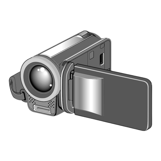
Dual Camera
Contents
1. OUTLINE OF CIRCUIT DESCRIPTION ............................... 3
2. DISASSEMBLY ................................................................... 12
3. ELECTRICAL ADJUSTMENT ............................................. 18
4. USB STORAGE INFORMATION REGISTRATION ............ 25
5. TROUBLESHOOTING GUIDE ............................................ 26
6. PARTS LIST ........................................................................ 28
RoHS
•This product does not contain any hazardous substances prohibited by the RoHS
Directive.
WARNING
•You are requested to use RoHS compliant parts for maintenance or repair.
•You are requested to use lead-free solder.
(This product has been manufactured using lead-free solder. Be sure to follow the
warning given on page 2 when carrying out repair work.)
CAUTION : Danger of explosion if battery is incorrectly replaced.
Replace only with the same or equivalent type recommended by the
manufacturer.
Discard used batteries according to the manufacturer's instructions.
NOTE : 1. Parts order must contain model number, part number, and description.
2. Substitute parts may be supplied as the service parts.
3. N. S. P. : Not available as service parts.
Design and specification are subject to change without notice.
SG317/U, EX, GX, U2, EX2, GX2 (R)
FILE NO.
VPC-FH1BK
(Product Code : 168 176 02)
(U.S.A.) (Canada) (Taiwan) (General)
VPC-FH1EXBK
(Product Code : 168 176 03)
(Europe) (U.K.) (South America)
(China) (Australia) (Hong Kong)
(Russia) (Middle East) (Africa)
(General) (Korea) (Taiwan)
VPC-FH1GXBK
(Product Code : 168 176 04)
(South America) (China)
(Australia) (Hong Kong)
(General) (Korea) (Taiwan)
VPC-FH1
(Product Code : 168 176 06)
(U.S.A.) (Canada) (Taiwan) (General)
VPC-FH1EX
(Product Code : 168 176 07)
(Europe) (U.K.) (South America)
(China) (Australia) (Hong Kong)
(Russia) (Middle East) (Africa)
(General) (Korea) (Taiwan)
VPC-FH1GX
(Product Code : 168 176 08)
(South America) (China)
(Australia) (Hong Kong)
(General) (Korea) (Taiwan)
REFERENCE No. SM5310779
Advertisement
Chapters
Table of Contents

Related Manuals for Sanyo VPC-FH1BK


Summary of Contents for Sanyo VPC-FH1BK
-
Page 1: Table Of Contents
FILE NO. SERVICE MANUAL Dual Camera VPC-FH1BK (Product Code : 168 176 02) (U.S.A.) (Canada) (Taiwan) (General) VPC-FH1EXBK (Product Code : 168 176 03) (Europe) (U.K.) (South America) (China) (Australia) (Hong Kong) (Russia) (Middle East) (Africa) (General) (Korea) (Taiwan) VPC-FH1GXBK... - Page 2 PRODUCT SAFETY NOTICE The components designated by a symbol ( ! ) in this schematic diagram designates components whose value are of special significance to product safety. Should any component designated by a symbol need to be replaced, use only the part designated in the Parts List.
-
Page 3: Outline Of Circuit Description
OUTLINE OF CIRCUIT DESCRIPTION 1-1. CMOS CIRCUIT DESCRIPTION 1. IC Configuration The CMOS peripheral circuit block basically consists of the following ICs. IC911 (IMX039LQR) CMOS imager H driver, V driver, serial communication circuit built-in CDS/PGA built-in Gain + 18 dB (step pitch 0.1 dB) 10 bit/12 bit A/D converter built-in 2. - Page 4 1-2. CP1 and VF1 CIRCUIT DESCRIPTION 1. Circuit Description 2. Outline of Operation 1-1. Digital clamp When the shutter opens, the reset signals (ASIC and CPU) The optical black section extracts averaged values from the and the serial signals (“take a picture” commands) from the 8- subsequent data to make the black level of the sensor output bit microprocessor are input and operation starts.
- Page 5 4. Lens drive block 5. Video Clip Recording and Playback 4-1. Focus drive 5-1. Recording The 16-bit serial data signals (LENS_SDI) and (LENS_SCLK The signal from the camera block is input to IC101 (ASIC). The and LENS_EN) which are output from the ASIC (IC101) are data that is input to the ASIC is input to SDRAM, and converts used to drive (FOCUS A +, FOCUS A -, FOCUS B + and FO- this data to encoded MPEG4 data, after which it is written in...
- Page 6 1-3. PWA POWER CIRCUIT DESCRIPTION 1. Outline 3. Digital 3.25 V Power Output This is the main power circuit, and is comprised of the follow- VDD3 is output. Feedback for the VDD3 is provided to the ing blocks. swiching controller (Pin (F3) of IC501) so that PWM control Switching controller (IC501) can be carried out.
- Page 7 1-4. ST1 STROBE CIRCUIT DESCRIPTION 1. Charging Circuit 2. Light Emission Circuit When UNREG power is supplied to the charge circuit and the When FLCTL signal is input from the ASIC, the stroboscope CHG signal from microprocessor becomes High (3.3 V), the emits light.
- Page 8 1-5. SYA CIRCUIT DESCRIPTION 1. Configuration and Functions For the overall configuration of the SYA block, refer to the block diagram. The SYA block centers around a 8-bit microprocessor (IC301), and controls camera system condition (mode). The 8-bit microprocessor handles the following functions. 1.
- Page 9 BAT_TMP Battery temperature detection BAT_OFF Battery OFF detection signal input ZSREQ Serial communication request signal S1 key input KEY_1st IR_IN Remote controller input ZRESET Microprocessor reset input XCIN 32 k oscillation input XCOUT 32 k oscillation output Power VSS1 Power XOUT Power VDD1...
- Page 10 4. Power Supply Control The 8-bit microprocessor controls the power supply for the overall system. The following is a description of how the power supply is turned on and off. When the battery is attached, a regulated 3.2 V voltage is normally input to the 8-bit microprocessor (IC301) by IC302, so that clock counting and key scanning is carried out even when the power switch is turned off, so that the camera can start up again.
- Page 11 MEMO – 11 –...
-
Page 12: Disassembly
2. DISASSEMBLY 2-1. REMOVAL OF CABINET BOTTOM, CABINET TOP, CABINET BACK, TB4 BOARD AND CABINET FRONT When assembling, When assembling, assemble order. tighten the screws order. A → B a → b → c When assembling, assemble order. A → B When assembling, tighten the screws order. - Page 13 1. Cover battery 50. Dec joint 2. Spacer bottom 42. Sheild tape mic 51. Dec line joint 3. Spacer LCD 52. Two screws 1.7 x 4 4. Spacer LCD front 53. Screw 1.7 x 3 5. Two screws 1.7 x 2 54.
- Page 14 2-2. REMOVAL OF TB1 BOARD, TB5 BOARD, LENS, ST1 BOARD, CP1 BOARD AND TB3 BOARD When assembling, tighten the screws order. a → b → c 21 22 When assembling, tighten the screws order. A → B 24, 26 When assembling, tighten the screws order.
- Page 15 1. Shield tape VF1 49. Spacer holder TB1 2. Screw 1.7 x 3 50. Three screws 1.7 x 2.5 3. Heat sink left 51. TB3 board 4. Heat sink tape top 52. Chassis right 5. Three screws 1.7 x 3 6.
- Page 16 2-3. REMOVAL OF TB2 BOARD, VF1 BOARD AND LCD 1. Screw 1.7 x 2 15. Spacer LCD FPC 18. Screw 1.7 x 2 21. Two screws 1.7 x 3 2. Screw 1.7 x 3 16. Remove the solder. 19. TB2 board 22.
- Page 17 2-4. BOARD LOCATION TB4 board TB1 board TB5 board TB3 board VF1 board CP1 board TB2 board ST1 board – 17 –...
-
Page 18: Electrical Adjustment
Download the calibration software and the firmware 3-4. Setup from the following URL. 1. System requirements http://www.digital-sanyo.com/overseas/service/ Windows 2000 or XP or Vista Place the DscCalDi.exe file, camapi32.dll file and IBM R -compatible PC with pentium processor QrCodeInfo.dll file together into a folder of your USB port choice. - Page 19 3-6. The adjustment item which in necessary in part exchange CMOS Black Lens CMOS Lens Lens Mecha Point And Adjust- White Point Factory Adjust- Adjust- Shutter White Point Language storage Reset ment Defect Adjust- Cord Defect Detect Setting ment ment Adjust- information Setting...
- Page 20 2. Lens Adjustment (Infinity) Adjustment value determination is effectuated using below val- ues. The adjustment values fulfill the conditions below, they are de- termined as within specifications. Adjustment value determination AF_TEMP_AD_I: ATADI ATADI: adjustment value of focus temperature A/D (250<=ATADI<=893) PZ_BR: PBR PBR: adjustment value of zoom backrush pulse (0<=PBR<=10)
- Page 21 3. Lens Adjustment (1m) Adjustment value determination AF_TEMP_AD: ATAD ATAD: adjustment value of focus temperature A/D (250<=ATAD<=893) AF_WIDE: ZW ZW: adjustment value of focus at zoom position wide (–300<=ZW<=300) AF_MID1: ZM1 ZM1: adjustment value of focus at zoom position middle1 (–300<=ZM1<=300) AF_MID2: ZM2 ZM2: adjustment value of focus at zoom position middle2...
- Page 22 5. WB Adjustment 3. Double-click on the DscCalDi.exe. 4. Input “32” in the Cal Mode, and click Ok at the right side. 5. Click the OK. 6. Input “30” in the Cal Mode, and click Ok at the right side. 7.
- Page 23 3-9. Factory Code Setting Adjustment value determination wc0=128 ± 2, wc1=128 ± 2, wc2<=255 1. Check the "Factory Code" display within the Setting group. wnc0=128 ± 2, wnc1=128 ± 2, wnc2<=255 2. For U.S.A., Canada and NTSC general area Adjustment values other than the above are irrelevant. If "FC_SANYO_U"...
- Page 24 3-13. Firmware uploading procedure 1. Uploading the firmware should be carried out if the version number (COMPL PWB XX-X) on the replacement circuit board is lower than the version of the distributed firmware. For XX-X, enter the name of the circuit board containing the firmware.
-
Page 25: Usb Storage Information Registration
18.) 2. Double-click on the DscCalDi.exe. 3. Click on the Get button in the USB storage window and check the USB storage data. VID: SANYO PID: FH1 Serial: Rev. : 1.00 4. -
Page 26: Troubleshooting Guide
5. TROUBLESHOOTING GUIDE POWER LOSS INOPERTIVE TAKING INOPERATIVE PUSH SHUTTER PUSH THE POWER BUTTON SW FOR A WHILE IC301-51, 23 IC301-43 CHECK S3003 (KEY_1st, KEY_2nd) CHECK SW UNIT (SCAN OUT1) LEVEL INPUT PULSE INPUT IC501-F6 (PON) CHECK IC301, IC101, IC302-7 5.3 V IC503-4 (PAON2) CHECK IC501 PWA BLOCK... - Page 27 MEMO – 27 –...
-
Page 28: Parts List
636 124 5289 INSTRUCTION MANUAL,CAMERA SOFT GB, CAMERA (English) 9056 636 121 1925 INSTRUCTION MANUAL,Xacti library(English) 636 124 5890 CARTON INNER-SG317/EX, EXCEPT VPC-FH1BK,VPC-FH1 636 124 5883 CARTON INNER-SG317/U, VPC-FH1BK,VPC-FH1 636 077 8139 CUSHION SHEET-SX774/KRO 636 122 9326 REINFORCE PAD,A-SG314/J 636 119 2361... - Page 30 LOCATION PARTS NO. DESCRIPTION LOCATION PARTS NO. DESCRIPTION 636 121 4964 COVER DC-SG314/J, CABINET & CHASSIS PARTS 1 VPC-FH1BK,VPC-FH1EXBK,VPC-FH1GXBK 636 125 8289 LABEL CAUTION-SG217/U 636 124 8006 COVER DC-SG317/J2, 636 125 6056 ASSY,CABI BOTTOM-SG317, VPC-FH1,VPC-FH1EX,VPC-FH1GX VPC-FH1BK,VPC-FH1EXBK,VPC-FH1GXBK 411 178 9403 SCR S-TPG PAN PCS 1.7X4.0,...
- Page 31 Cabinet 1 SG317/J PARTS LIST 1...
- Page 32 636 121 5336 ASSY,JOINT-SG314/J 636 106 6310 ASSY,SHIELD WIRE CP1-VF1 636 127 4586 SHIELD TAPE VF1-SG317 636 127 2667 ASSY,COVER LCD B SV-SG317, VPC-FH1BK,VPC-FH1EXBK,VPC-FH1GXBK 636 127 2681 ASSY,COVER LCD B SV-SG317, VPC-FH1,VPC-FH1EX,VPC-FH1GX 636 122 6950 COMPL PWB,TB-2 636 124 8181 COVER JOINT-SG317/J,...
- Page 33 85 114 Cabinet 2 SG317/J PARTS LIST 1...
- Page 34 ELECTRICAL PARTS Note: 1. Materials of Capacitors and Resistors are abbreviated as follows ; Resistors Capacitors MT-FILM Metallized Film Resistor MT-POLYEST Metallized Polyester Capacitor MT-GLAZE Metallized Glaze Resistor MT-COMPO Metallized Composite Capacitor OXIDE-MT Oxide Metallized Film Resistor TA-SOLID Tantalum Solid Capacitor AL-SOLID Aluminum Solid Capacitor NP-ELECT...
- Page 35 LOCATION PARTS NO. DESCRIPTION LOCATION PARTS NO. DESCRIPTION D5204 307 248 0701 DIODE MA21D3800 C1302 303 381 8109 CERAMIC 1U K 6.3V D5301 307 248 0701 DIODE MA21D3800 C1303 303 381 8109 CERAMIC 1U K 6.3V (OSCILLATORS) C1304 303 409 3406 CERAMIC 0.1U K 16V X1102...
- Page 36 LOCATION PARTS NO. DESCRIPTION LOCATION PARTS NO. DESCRIPTION C5206 303 433 1102 CERAMIC 1U K 10V R1501 301 224 9306 MT-GLAZE 1K JA 1/16W C5207 303 433 1102 CERAMIC 1U K 10V R1502 301 263 2009 MT-GLAZE 8.2K DC 1/16W C5208 303 433 1102 CERAMIC...
- Page 37 LOCATION PARTS NO. DESCRIPTION LOCATION PARTS NO. DESCRIPTION R5058 301 240 9601 MT-GLAZE 680K JA 1/16W F5008 323 031 1502 FUSE 32V 1A R5059 301 224 8903 MT-GLAZE 100K JA 1/16W (JACK) R5062 301 224 9009 MT-GLAZE 10K JA 1/16W JK501 645 086 0430 SOCKET,DC 3P...
- Page 38 LOCATION PARTS NO. DESCRIPTION LOCATION PARTS NO. DESCRIPTION (RESISTORS) COMPL PWB,TB-2 R1701 301 226 1506 MT-GLAZE 0.000 ZA 1/16W 636 122 6950 R1702 301 228 4505 MT-GLAZE 2.2 JA 1/16W R1703 301 224 8903 MT-GLAZE 100K JA 1/16W (SWITCH) (CONNECTORS) S6501 645 092 3159 SWITCH,PUSH 1P-1TX1...
-
Page 39: Circuit Diagrams & Printed Wiring Boards
CIRCUIT DIAGRAMS & PRINTED WIRING BOARDS TABLE OF CONTENTS OVERALL WIRING & BLOCK DIAGRAMS Page OVERALL WIRING .............................C3 OVERALL CIRCUIT ............................C4 POWER CIRCUIT...............................C4 IMAGE SENSOR CIRCUIT ..........................C5 LENS CIRCUIT ..............................C5 MAIN CIRCUIT ..............................C6 SYSTEM CONTROL CIRCUIT ......................... C7 STROBE CIRCUIT .............................C7 CIRCUIT DIAGRAMS CP1 BOARD (PWA) POWER ..........................C8 CA1 BOARD IMAGE SENSOR ........................ - Page 40 NOTES: 1. All resistance values in "OHMS" unless otherwise noted. (K=1,000 ; M=1,000,000) 2. All capacitance values in "µF" unless otherwise noted. p=pico farad ; n=nano farad ; µ ,u or U=micro farad 3. All inductance values in "µH" unless otherwise noted. µ...
-
Page 41: Overall Wiring & Block Diagrams
OVERALL WIRING & BLOCK DIAGRAMS OVERALL WIRING SPEAKER FLASH REFLECTOR LENS TRANS TRIGGER CN105 CN541 AL3.2V AL3.2V AL3.2V AL3.2V JW183 FLCTL FLCTL MIC(R) ZCHGDONE ZCHGDONE YELLOW BOOST5V BOOST5V JW184 BOOST5V BOOST5V A_GND IR_VDD IR_VDD IR_IN IR_IN GRAY IR_GND IR_GND JW181 MIC(L) WHITE UNREGST... -
Page 42: Overall Circuit
POWER CIRCUIT OVERALL CIRCUIT TO DMA USB_VBUS LENS UNIT CHG_CNT IC521 12,13 x10 F1.8 POWER_IN, DC_IN BATTERY CHARGE TO SYA TIME OUT BAT+ BAT+SY Q5010,Q5011 CN951 TO SYA USB_VBUS TO DMA CA1 BOARD CP1 BOARD USB_5VON TO DMA L5301 IC911 9ch-LVDS IC951 TO TCA,SYA... -
Page 43: Image Sensor Circuit
IMAGE SENSOR CIRCUIT LENS CIRCUIT LENS_TEMP IC101 A2.7V D1.8V I/O1.8V ZPI_AD FPI_AD SYSTEM ASIC VDD3 CN951 LENS_BLOCK TO DMA IC101 IC951 LENS DRIVER IRIS CONTROLLER THERMISTOR VM1,VM2,VM3, BOOST5V VM4,VCC VDD3 DCKP SCKIP0 ZOOM_PI IC952 OPVDD,ADVDD,DAVDD, DCKM SCKIN0 3.3V DVD33,ADVRH IC911 TO SYA IC301 Z_SENSE VDD1.8... -
Page 44: Main Circuit
MAIN CIRCUIT 48MHz IC111 ADCK CCDEN,CCDSD,CCDCK CLOCK GENERATOR 74.17582MHz, TGHD,TGVD 148.352MHz XCLR CN104 BOARD SCKIN0,SCKIP0 (LVDS) X1102 SDIP[0:7],SDIN[0:7] (LVDS) 48.000MHz PWA BLOCK POWER SUPPLY PAON1,PAON2,PAON3,BLON LENS_RESETN LENS SCLK,LENS EN, LENS SDI SHUTTER+,PS IC951 LENS SDO FPIOUT,ZPIOUT STATE1,STATE2 LENS DRIVER LENS CN951 CLK24M UNIT... -
Page 45: System Control Circuit
SYSTEM CONTROL CIRCUIT STROBE CIRCUIT BOOST 5V CHARGING CIRCUIT VDD2 ST_CHG ALWAYS 3.2V ST_CHG_ON BACKUP3.2V TO DMA VDD3 ZCHGDONE T5401 D5402 C5401 ZCHG_DONE VDD1 POWER FILTER OSCILLATION RECTIFIER C5412 IC302 TIMEOUT TRANSFORMER CIRCUIT BLOCK ZRESET TIMEOUT CN541 BATTERY BACKUP CHG_CNT VSS2 UNREGST 16:20... -
Page 46: Circuit Diagrams
CIRCUIT DIAGRAMS CP1 BOARD (PWA) POWER F5004 2A32V TO DMA UNREGST F47K2R0C3LFND TO SYA UNREGSY 1608 F5001 1608 1AV4J11B8060N 2A32V MJC-040-D1-2 L5001 D5007 FBMH1608HL300 JK501 RB060M-30 POWER IN UNREG F47K2R0C3LFND L5004 1608 Q5202 VDD1.2 SI3473DV R5208 1AV4L2WN2R0MG 1K;1/16J TO DMA 5.2X5.2 MA21D38 H=3.0... -
Page 47: Ca1 Board Image Sensor
MAIN CIRCUIT WAVEFORMS CA1 BOARD IMAGE SENSOR TEST POINT WAVEFORM LOCATION IC101 PIN AL25 XOUT 1V/div 10ns/div CN911 DGND DGND XCLR IC101 DGND SDIP7 SDIP7 PIN AE31 SDIN7 SDIN7 SDIP6 SDIP6 D4CKIN SDIN6 SDIN6 SDIP5 SDIP5 1V/div SDIN5 SDIN5 10ns/div SDIP4 SDIP4 TOUT8... -
Page 48: Cp1 Board (Dma) Main
CP1 BOARD (DMA) MAIN C1308 D1-17600/SG317-U CLK24M VOLTAGE: VIEW MODE, LCD ON TO PWA VDD3 VDD1.8 R1304 VA131 F5007 L1302 C1310 0.1;B 10K;1/16J AVR-M1608C120MT 2A32V FBMH1608HL300 USB_VDD L1301 IC132 1608 USB D(-) TC7WH32FK DACK C1311 QTC7WH32FK--K R1305 6.2K;1/16D DREQ USB D(+) IC131 EXC24CF900 ZAV_JACK... - Page 49 CP1 BOARD (DMA) MAIN [UPPER-LEFT] D1-17600/SG317-U VOLTAGE: VIEW MODE, LCD ON VDD1.8 VDD1.2 VDD3 AD25 AC25 AL26 AJ17 AE25 AE24 AE14 AA21 AA18 AA17 AA14 AA13 C1063 0.1;B C1051 0.1;B C1057 0.1;B C1064 0.1;B C1052 0.1;B C1058 C1065 0.1;B C1053 0.1;B 0.1;B C1066...
- Page 50 CP1 BOARD (DMA) MAIN [UPPER-RIGHT] C1308 CLK24M B5 VSS CLKIN TO PWA VDD3 D7 CVDD LVDD VDD1.8 C1310 R1304 VA131 F5007 L1302 H5 CD2 0.1;B 10K;1/16J AVR-M1608C120MT 2A32V FBMH1608HL300 USB_VDD G5 CD1 1608 L1301 USB D(-) IC132 H4 CD0 TC7WH32FK C1311 QTC7WH32FK--K DACK...
- Page 51 FLCTL EV3HB ZCHGDONE ZCHGDONE ST_CHG BOOST5V BOOST5V BOOST5V QEV3HB------N IR_VDD TO SYA SW3.2V IR_IN IR_IN IR_GND CP1 BOARD (DMA) MAIN [LOWER-LEFT] SYSTEM ASIC UNREGST UNREGST ZUSB_DET UNREGST TO PWA UNREGST HOTLINE ZBOOT_COMREQ H=1.35 UNREGST ASIC_SDO UNREGST ASIC_SDI TO ST1 CN541 ASIC_SCK MRST IR_IN...
- Page 52 EV3HB VDDQ DQP29 DQP29 DQS31 DQS16 DQ31 DQ16 DQP30 DQP30 C1038 0.1;B DQP31 VSSQ DQP31 DQS17 VDDQ DQ17 DAP0 DAP0 DQS18 EV3HB------N DQS29 DQ29 DQ18 DAP1 DAP1 DQS30 DAP2 DQ30 VSSQ DAP2 DQS19 VSSQ DQ19 DAP3 DAP3 DQS27 DQS20 CP1 BOARD (DMA) MAIN [LOWER-RIGHT] DQ27 DQ20 DAP4...
-
Page 53: Cp1 Board (Dmb) Hdmi
CP1 BOARD (DMB) HDMI VDD1.8 TO DMB D2-17600/SG317-U C1907 1608 CN191 TMDS SHLD2 C1908 L1901 TMDS DATA2+ 0.1;B DLP2ADN900HL4 TMDS DATA2- VSSA TMDS SHLD1 TX2+ TMDS DATA1+ TX2- TMDS DATA1- A_I2CSDATA A_I2CSDATA VDDA(TMDS)(1V8) TMDS SHLD0 A_I2CSCLK A_I2CSCLK Tx1+ TMDS DATA0+ L1902 Tx1- DLP2ADN900HL4... -
Page 54: Cp1 Board (Tca) Lens
CP1 BOARD (TCA) LENS BOOST5V TO PWA F1-17600/SG317-U 3.3V REG IC952 XC6221S04XG QXC6221S04XGP VOUT TO SYA VDD3 R9505 ZPI_AD CN951 0;1/16Z ZOOM_PI_E Z_SENSE RB951 ZOOM_PI_K PILED ZOOM_PI_AC VDD3 VDD3 VDD1.8 TO PWA HALL_IN+ HALL_IN+ HALL_OUT- HALL_OUT+ HALL_OUT+ HALL_OUT- HALL_IN- HALL_IN- LENS_SCLK C4 MCLK R9502... -
Page 55: Cp1 Board (Sya) System Control
CP1 BOARD (SYA) SYSTEM CONTROL TO DMA AL3.2V AL3.2V BOOST5V BOOST5V BOOST5V UNREGSY TO PWA UNREGSY SW3.2V SW3.2V TO DMA Y1-17600/SG317-U IR_IN TO DMA ZSREQ VOLTAGE: VIEW MODE, LCD ON R3005 10K;1/16D BAT_TEMP TO PWA SW3.2ON DC_IN TO PWA UP0431300 Q3003 AL3.2V AL3.2V... -
Page 56: Tb5 Board Av Treminal
ST1 BOARD STROBE TB5 BOARD AV TERMINAL STROBE UNIT FLASH REFLECTOR TO TB1 CN632 CN641 T5-17600/SG317-U T5401 VOLTAGE: STROBE AFTER CHARGE TTRN-0530H-018-T S1-17600/SG317-U LINE2 JW541 AWG30 Pb_GND BROWN D5402 2.0X1.25 Pb_OUT RE0208DA 1AV4L17B0450N STROBE CHARGE Y_GND T5402 R5435 TS-F35A-3 IC541 R5431 100;1/16J 100;1/16J... -
Page 57: Tb1 Board Sd Card Socket
TB1 BOARD SD CARD SOCKET VF1 BOARD LCD CONNECTOR CN631 MEMCLK CN172 Z1-17600/SG317-U MEMCLK CN171 MEMCMD MEMCMD MEMDATA3 VDD3 VDD3 LCDRESET GREST MEMDATA3 RB171 RB171 RB171 RB171 T1-17600/SG317-U MEMDATA2 MEMDATA2 R1701 LCDD0 LCDD0 SHDB MEMDATA1 MEMDATA1 MEMDATA0 MEMDATA0 LCDD1 LCDD1 LCDEN 0;1/16Z SCEN... -
Page 58: Printed Wiring Boards (P.w.b.)
PRINTED WIRING BOARDS (P.W.B.) CP1 P.W.B. (SIDE A) CN191 CN302 C1035 BAT- IC102 VA132 VA133 VA134 R5022 R1901 C5072 R5023 L1901 L1902 R1934 R1936 R1935 C1067 C1007 VA101 R1915 C1016 Q5007 Q5008 C1032 C1033 C1005 C1038 BAT_T D5003 R1922 C1044 C1043 C1066 C1010... -
Page 59: Cp1 P.w.b. (Side B)
CP1 P.W.B. (SIDE B) Q5020 R5055 R5056 Q5019 JK501 R5059 X1901 L5001 R5087 Q5013 C1911 CN103 Q5010 C1905 C1904 D5007 R5033 R5069 D5301 C5301 R1925 R5067 R5068 C5303 R1302 C1307 R1924 C1906 Q5011 R5302 R5301 C5302 C5067 R5303 R5001 Q5021 VA302 C1303 R5304... - Page 60 CA1 P.W.B. (SIDE A) CA1 P.W.B. (SIDE B) TB3 P.W.B. (SIDE B) TB3 P.W.B. (SIDE A) C6101 R9111 C9127 C9125 C9119 R9112 C9128 C9121 C9116 R9106 C9118 C9132 IC911 C9122 C9101 C9112 CL911 C9129 C9114 C9123 C9126 CN911...
-
Page 61: Tb1 P.w.b. (Side A & B)
TB2 P.W.B. (SIDE A) TB2 P.W.B. (SIDE B) TB1 P.W.B. (SIDE A) TB1 P.W.B. (SIDE B) C1557 R1431 C1556 C1558 IC155 C1559 R1554 C1560 C1553 C1410 C1552 C1561 C1401 C1551 R1402 C1254 CN141 RB142 R1401 RB143 C1406 RB141 RB125 RB126 J3000CA C1251 SIDE-A... -
Page 62: Tb4 P.w.b. (Side A & B)
TB4 P.W.B. (SIDE A) TB4 P.W.B. (SIDE B) S6201 S6203 CN622 SG317 SG31A_TB4 J3000FA SIDE-A S6205 SIDE-B CN621 TB5 P.W.B. (SIDE A) TB5 P.W.B. (SIDE B) R6401 VA641 L6401 L6402 SG317/SG31A_TB5 SG317/SG31A_TB5 R6402 R6403 J3000GA J3000GA R6404 SIDE-A SIDE-B... - Page 63 VF1 P.W.B. (SIDE A) ST1 P.W.B. (SIDE A) VF1 P.W.B. (SIDE B) ST1 P.W.B. (SIDE B) R5433 CL560 CL561 C5434 R5432 R5435 D5404 C5435 R5431 C1701 Q5402 C5411 D5401 C5412 J3000BA SG317/31A-ST1...
- Page 65 SANYO Electric Co., Ltd. Osaka, Japan Feb./’09...
Need help?
Do you have a question about the VPC-FH1BK and is the answer not in the manual?
Questions and answers