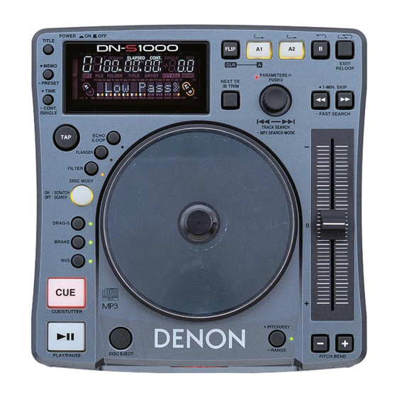
Denon DN-S1000 Service Manual
Table top single cd player
Hide thumbs
Also See for DN-S1000:
- Operating instructions manual (36 pages) ,
- Operating instructions manual (35 pages) ,
- Operating instructions manual (35 pages)
Table of Contents
Advertisement
QQ
3 7 63 1515 0
TE
L 13942296513
For purposes of improvement, specifications and
●
design are subject to change without notice.
Please use this service manual with referring to the
●
operating instructions without fail.
Some illustrations using in this service manual are
●
slightly different from the actual set.
www
.
http://www.xiaoyu163.com
SERVICE MANUAL
MODEL
TABLE TOP SINGLE CD PLAYER
x
ao
u163
y
i
http://www.xiaoyu163.com
2 9
8
For U.S.A., Canada, Europe, U.K.,
Asia, China, Taiwan R.O.C., Korea
& Japan model
DN-S1000
Q Q
3
6 7
1 3
1 5
注 意
サービスをおこなう前に、このサービスマニュアルを
必ずお読みください。本機は、火災、感電、けがなど
に対する安全性を確保するために、さまざまな配慮を
おこなっており、また法的には「電気用品安全法」に
もとづき、所定の許可を得て製造されております。
従ってサービスをおこなう際は、これらの安全性が維
持されるよう、このサービスマニュアルに記載されて
いる注意事項を必ずお守りください。
本機の仕様は性能改良のため、予告なく変更すること
●
があります。
補修用性能部品の保有期間は、製造打切後8年です。
●
修理の際は、必ず取扱説明書を参照の上、作業を行っ
●
てください。
本文中に使用しているイラストは、説明の都合上現物
●
と多少異なる場合があります。
co
.
TOKYO, JAPAN
9 4
2 8
Ver. 1
0 5
8
2 9
9 4
2 8
m
X0208V.01 DE/CDM 0408
9 9
9 9
Advertisement
Table of Contents

Related Manuals for Denon DN-S1000


Summary of Contents for Denon DN-S1000
- Page 1 3 7 63 1515 0 For U.S.A., Canada, Europe, U.K., Asia, China, Taiwan R.O.C., Korea & Japan model Ver. 1 SERVICE MANUAL DN-S1000 MODEL TABLE TOP SINGLE CD PLAYER L 13942296513 注 意 サービスをおこなう前に、このサービスマニュアルを 必ずお読みください。本機は、火災、感電、けがなど に対する安全性を確保するために、さまざまな配慮を おこなっており、また法的には「電気用品安全法」に もとづき、所定の許可を得て製造されております。 従ってサービスをおこなう際は、これらの安全性が維 持されるよう、このサービスマニュアルに記載されて...
-
Page 2: Laser Radiation
DN-S1000 3 7 63 1515 0 SAFETY PRECAUTIONS The following check should be performed for the continued protection of the customer and service technician. LEAKAGE CURRENT CHECK Before returning the unit to the customer, make sure you make either (1) a leakage current check or (2) a line to chassis resistance check. -
Page 3: Te L 13942296513
DN-S1000 DISASSEMBLY 3 7 63 1515 0 (Follow the procedure below in reverse order when reassembling.) 1. Bottom Plate (1) Remove 6 screws 57 and pull out Bottom Plate. Bottom Plate L 13942296513 2. Top Cover unit (1) Remove 6 screws 61 and 2 screws 59. - Page 4 DN-S1000 3. Shield Bracket 3 7 63 1515 0 (1) Remove 4 screws 58 and 2 screws 67. (2) Detach Shield Bracket. Shield Bracket 4. Mecha unit (1) Remove 2 screws 53 and 2 screws 55. (2) Disconnect FFC cable.
- Page 5 DN-S1000 5. Power P.W.B. 3 7 63 1515 0 (1) Remove 5 screws 58, a screws 60 and a screws 61. (2) Detach Power P.W.B. Power P.W.B. 6. Main P.W.B. L 13942296513 (1) Short-circuit the short land above. (2) Remove a screws 54 and a screws 56.
- Page 6 DN-S1000 7. CD Mecha 3 7 63 1515 0 (1) Remove 2 screws 53 and pull out Main Pwb Bracket. (2) Remove 2 screws 55 and pull out Disc Guide. Main Pwb Bracket CD Mecha Disc Guide L 13942296513 8.
- Page 7 DN-S1000 9. Disc Switch P.W.B. 3 7 63 1515 0 (1) Detach Slip mat, Anti-Static Sheet and Spring Plate. (2) Remove 4 screws 56. (3) Detach Disc Switch P.W.B. Slip Sheet Anti-Static Sheet Slip mat Spring Plate Disc Switch P.W.B.
-
Page 8: Block Diagram
DN-S1000 BLOCK DIAGRAM 3 7 6 3 1 5 1 5 0 MAIN UNIT POWER UNIT X'tal 11.2M LV393 Analog Out PCM1748 SDRAM Digital Out ABCK/ALRCK DBCK/DLRCK SERVO DSP Driver ±5VA MN6627933 AN8785BS Power Head Amp BCK/LRCK CD MECHA AN2002A 3.3V... -
Page 9: Confirming The Servo
1. Contents of Service Program 1. サービス プログラムの内容 Turn on the power while pressing both B button and the PARAMETER knob to set the service mode of DN-S1000. Turn on the power DN-S1000 は B ボタンとパラメータノブを両方押しながら、電源を投入するとサービスモードになります。DN-D6000 は CD1 のパラメータノブと while pressing both PARAMETER knob of CD1 and "LOOP B" button of CD2 to set the service mode of DN-D6000. The various CD2 の... - Page 10 DN-S1000 3 7 6 3 1 5 1 5 0 CUE button FLT all light check performed while button pressed. CUE ボタン ボタンを押している間、FLT の全点灯チェックを行います。 BEND+ button FLT all off check performed while button pressed. BEND+ ボタン ボタンを押している間、FLT の全消灯チェックを行います。 BEND- button Disc eject status set while button pressed.
- Page 11 **** E **** エラーコード 4. µcom update 4. マイコンアップデート With the DN-S1000 and DN-D6000, the system µcom and DSP can be updated from a disc. DN-S1000、DN-D6000 は、ディスクから、システムマイコン、DSP のアップデートを行うことができます。 (1) Creating the update disc (1) アップデートディスクの作成 Use the procedure described below to create the disc for updating the system microprocessor and DSP.
- Page 12 DN-S1000 3 7 63 1515 0 SEMICONDUCTORS /半導体一覧表 Only major semiconductors are shown, general semiconductors etc. are omitted to list. 主な半導体を記載しています。汎用の半導体は記載を省略しています。 1. IC’s MN102H730F (IC101) TOP VIEW MN102H730F Terminal Function L 13942296513 Pin Name Simbol I/O DET Function CS0_ CS0_ Ext.
- Page 13 DN-S1000 3 7 63 1515 0 Pin Name Simbol I/O DET Function Power (+3.3V) OSCI OSCI Oscillation input, 32.0MHz OSCO OSCO Oscillation output P57,BOSC RESERVE PC5,NMI_ Connect to Power RST_ RST_ µcom reset _MUTE Mute signal (L: Mute) RESERVE...
- Page 14 DN-S1000 3 7 63 1515 0 Pin Name Simbol I/O DET Function KIN0 DNS1000: Key scan input signal 0 EJECT DND6000: Disc eject button input signal KIN1 DNS1000: Key scan input signal 1 CDSEL DND6000: CD mecha. Select H: CD1, L: CD2...
- Page 15 DN-S1000 3 7 63 1515 0 ADSP-BF531 (IC401) PIN 1 TOP VIEW ADSP-BF531 Terminal Function Pin Name Symbol I/O DET Ext Ini Res Function VROUT2 Ext. FET drive output 2 VROUT1 VROUT1 Ext. FET drive output 1 VDDEXT VDDEXT I/O power supply (+3.3V)
- Page 16 DN-S1000 3 7 63 1515 0 Pin Name Symbol I/O DET Ext Ini Res Function VDDEXT VDDEXT I/O power supply (+3.3V) DSPF3 Programmable flag 5, Flag 3 to µcom (RESERVE) DSPF2 Programmable flag 4, Flag 2 to µcom (RESERVE) DSPF1 Programmable flag 3, Flag 1 to µcom (RESERVE)
- Page 17 DN-S1000 3 7 63 1515 0 Pin Name Symbol I/O DET Ext Ini Res Function BMODE1 BMODE1 Boot mode strap 1 BMODE0 BMODE0 Boot mode strap 0 DATA15 Ext. bus data 15 DATA14 Ext. bus data 14 100 DATA13 Ext.
- Page 18 DN-S1000 3 7 63 1515 0 Pin Name Symbol I/O DET Ext Ini Res Function 150 _ABE1 SDQM1 SDRAM data mask 1 151 _ABE0 SDQM0 SDRAM data mask 0 152 _AWE Async memory write enable 153 _ARE _ARE Async memory read enable...
- Page 19 DN-S1000 3 7 63 1515 0 MN6627933 (IC201) L 13942296513 MN6627933 Terminal Function Pin Name Function SDRAM data signal I/O 11 SDRAM data signal I/O 10 SDRAM data signal I/O 9 SDRAM data signal I/O 8 UDQM SDRAM higher rank byte data mask signal output...
- Page 20 DN-S1000 3 7 63 1515 0 Pin Name Function SDRAM chip select signal output SDRAM address signal output 3 SDRAM address signal output 2 SDRAM address signal output 1 SDRAM address signal output 0 DRVDD1 Power supply 1 for SDRAM interface I/O...
- Page 21 DN-S1000 3 7 63 1515 0 Pin Name Function MDATA µcom command data signal input µcom command load signal input *STAT Status signal output *BLKCK Subcode block clock signal output *SMCK 4.2336MHz/8.4672MHz clock signal output *PMCK 88.2kHz clock signal output...
- Page 22 DN-S1000 3 7 63 1515 0 M66005AFP (IC601) D I G D I G D I G D I G D I G D I G D i s p l a y C o d e R e g i s t e r...
- Page 23 DN-S1000 3 7 63 1515 0 AN8785SB (IC202) L: All mute [ Others ] Hiz: ch2,4 ON [ Loading ] [ Spindle ] [ Traverse ] [ Focus ] [ Tracking ] H: Active Standby PVcc2 PVcc3 PVcc1 Protection...
- Page 24 DN-S1000 3 7 63 1515 0 PCM1748 (IC106) DATA LRCK DGND PCM1748 ZEROL/NA ZEROR/ZEROA AGND Serial LRCK Output Amp and Input Low-Pass Filter DATA Enhanced Oversampling Multi-Level Digital Filter Delta-Sigma with Modulator Function Controller Output Amp and Function Control...
-
Page 25: Top View
DN-S1000 3 7 63 1515 0 64M SDRAM (IC210) 128M SDRAM (IC402) Pin Assignment Pin No. Pin Name Function Description 22, 23~26, A0~A11 Address Multiplexed pins for row and column address. 29~35 Row address: A0~A11. Column address: A0~A8. 20, 21... - Page 26 DN-S1000 2. FL DISPLAY 13-MT-99GN (FL601) 3 7 63 1515 0 Pin Connection L 13942296513 Grid Assignment u163 http://www.xiaoyu163.com...
- Page 27 DN-S1000 3 7 63 1515 0 Segment Designation Anode Connection L 13942296513 u163 http://www.xiaoyu163.com...
-
Page 28: Printed Wiring Boards
DN-S1000 PRINTED WIRING BOARDS 3 7 6 3 1 5 1 5 0 GU-3607 MAIN P.W.B. UNIT 1 3 9 4 2 2 9 6 5 1 3 COMPONENT SIDE FOIL SIDE w w w u 1 6 3... - Page 29 DN-S1000 3 7 6 3 1 5 1 5 0 GU-3608 PANEL P.W.B. UNIT 1 3 9 4 2 2 9 6 5 1 3 w w w u 1 6 3 COMPONENT SIDE http://www.xiaoyu163.com...
- Page 30 DN-S1000 3 7 6 3 1 5 1 5 0 1 3 9 4 2 2 9 6 5 1 3 w w w u 1 6 3 FOIL SIDE http://www.xiaoyu163.com...
-
Page 31: Note For Parts List
DN-S1000 3 7 63 1515 0 NOTE FOR PARTS LIST Part indicated with the mark " " are not always in stock and possibly to take a long period of time for supplying, or in some case supplying of part may be refused. -
Page 32: Parts List Of P.w.b. Unit
DN-S1000 PARTS LIST OF P.W.B. UNIT 3 7 63 1515 0 *本表に記載されている部品は、補修用部品のため製品に使用している部品とは一部、形状、寸法などが異なる場合があります Note: The symbols in the column "Remarks" indicate the following destinations. E3: U.S.A. & Canada model E2: Europe model JP: Japan model GU-3607 MAIN P.W.B. UNIT ASS'Y Ref. - Page 33 DN-S1000 3 7 63 1515 0 Ref. No. Part No. Part Name Remarks Q'ty C114 00D 254 4302 916 CE04W1A100MT(SRE) C115 00D 257 0509 929 CK73B1H102KT +1608 C116 00D 257 0512 903 CK73F1E104ZT +1608 C117 00D 254 4533 918...
- Page 34 DN-S1000 3 7 63 1515 0 Ref. No. Part No. Part Name Remarks Q'ty C239 00D 257 0510 947 CK73B1H562KT +1608 C240 00D 257 0516 909 CK73B1E223KT +1608 C241 00D 257 0501 927 CK73B1H153KT +1608 C242 00D 257 0506 919...
- Page 35 DN-S1000 3 7 63 1515 0 Ref. No. Part No. Part Name Remarks Q'ty X101 00D 399 0880 900 CSTLS32M0X53 X102 00D 399 0907 003 X'TAL(11.2896MHZ) X201 00D 399 0978 906 CSTCG25M0V53-R0 X401 00D 399 0978 906 CSTCG25M0V53-R0 L 13942296513 u163 http://www.xiaoyu163.com...
- Page 36 DN-S1000 GU-3608 PANEL P.W.B. UNIT ASS'Y 3 7 63 1515 0 Ref. No. Part No. Part Name Remarks Q'ty SEMICONDUCTORS GROUP IC601 00D 262 3228 908 M66005AFP IC602 00D 262 2745 903 BU2090F(E2) IC603 00D 262 2514 901 SN74LV138APW-EL2...
- Page 37 DN-S1000 3 7 63 1515 0 Ref. No. Part No. Part Name Remarks Q'ty CAPACITORS GROUP C601 00D 257 0512 903 CK73F1E104ZT +1608 C603,604 00D 257 0512 903 CK73F1E104ZT +1608 C605 00D 257 0506 951 CC73CH1H101JT +1608 C606 00D 257 0511 920...
- Page 38 DN-S1000 3 7 63 1515 0 Ref. No. Part No. Part Name Remarks Q'ty FH805 00D 202 0040 909 FUSE CLIP (TAPE) FL601 00D 393 8076 006 FLT(13-MT-99GN) JK751 00D 204 8664 008 3P PIN JACK JK753 00D 204 8416 007...
-
Page 39: Exploded View
DN-S1000 EXPLODED VIEW 3 7 6 3 1 5 1 5 0 Parts List 1 3 9 4 2 2 9 6 5 1 3 WARNING: Parts marked with this symbol have critical characteristics. Use ONLY replacement parts recommended by the manufacturer. -
Page 40: Parts List Of Exploded View
DN-S1000 PARTS LIST OF EXPLODED VIEW 3 7 63 1515 0 *本表に記載されている部品は、補修用部品のため製品に使用している部品とは一部、形状、寸法などが異なる場合があります。 Note: The symbols in the column "Remarks" indicate the following destinations. E3: U.S.A. & Canada model E2: Europe model JP: Japan model Ref. No. Part No. Part Name... - Page 41 DN-S1000 3 7 63 1515 0 Ref. No. Part No. Part Name Remarks Q'ty 00D 206 2085 003 AC CORD W/CON.DOM for JP 00D 415 0790 062 UL TUBE (14.3) BK for E2,JP for Ac cord 00D GEN 6760 F.CAUTION LABEL SUB...
-
Page 42: Exploded View Of Cd Mechanism
DN-S1000 EXPLODED VIEW OF CD MECHANISM 3 7 63 1515 0 L 13942296513 u163 http://www.xiaoyu163.com... -
Page 43: Parts List Of Cd Mechanism Unit
DN-S1000 PARTS LIST OF CD MECHANISM UNIT 3 7 63 1515 0 *本表に記載されている部品は、補修用部品のため製品に使用している部品とは一部、形状、寸法などが異なる場合があります。 Ref. No. Part No. Part Name Remarks Q'ty 00D 964 0012 006 SVP-CHCL 00D 964 0012 103 SVP-GD 00D 964 0012 200 SVP-ROLL 00D 964 0012 307... -
Page 44: Packing View
DN-S1000 PACKING VIEW 3 7 63 1515 0 203 ~ 208 L 13942296513 PARTS LIST OF PACKING & ACCESSORIES *本表に記載されている部品は、補修用部品のため製品に使用している部品とは一部、形状、寸法などが異なる場合があります。 Note: The symbols in the column "Remarks" indicate the following destinations. E3: U.S.A. & Canada model E2: Europe model JP: Japan model Ref. -
Page 45: Wiring Diagram
DN-S1000 WIRING DIAGRAM 3 7 6 3 1 5 1 5 0 SLOT IN CD MECHA MAIN UNIT PANEL UNIT 25P FFC STRAIGHT 25P FFC SIDE GU-3607 GU-3608-1 CD11-02 12PFFC CX121 CX251 CY251 DISC SENSOR UNIT SLED- _PDATA _PDATA... -
Page 46: Note For Schematic Diagram
DN-S1000 NOTE FOR SCHEMATIC DIAGRAM 3 7 63 1515 0 配線図について WARNING: ! 印の部品は安全を維持するために重要な部品です。 Parts marked with this symbol ! have critical characteristics. 従って交換時は必ず指定の部品を使用してください。 Use ONLY replacement parts recommended by the manufactur- 注) CAUTION: (1) 指定なき抵抗値は Ω、k は kΩ、M は MΩ を示す。... - Page 47 DN-S1000 SCHEMATIC DIAGRAMS (1/3) 3 7 6 3 1 5 1 5 0 1 3 9 4 2 2 9 6 5 1 3 w w w u 1 6 3 SIGNAL LINE SCHEMATIC DIAGRAMS (1/3) GU-3607 MAIN UNIT (1/2)
- Page 48 DN-S1000 SCHEMATIC DIAGRAMS (2/3) 3 7 6 3 1 5 1 5 0 1 3 9 4 2 2 9 6 5 1 3 w w w u 1 6 3 SIGNAL LINE SCHEMATIC DIAGRAMS (2/3) GU-3607 MAIN UNIT (2/2)
- Page 49 DN-S1000 SCHEMATIC DIAGRAMS (3/3) 3 7 6 3 1 5 1 5 0 1 3 9 4 2 2 9 6 5 1 3 SIGNAL LINE w w w SCHEMATIC DIAGRAMS (3/3) u 1 6 3 GU-3608-1 PANEL UNIT...
Need help?
Do you have a question about the DN-S1000 and is the answer not in the manual?
Questions and answers