Pioneer AVH-P6500DVD UC Service Manual
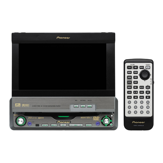
Av receiver/dvd player with 6.5 inch wide display
Hide thumbs
Also See for AVH-P6500DVD UC:
- Operation manual (109 pages) ,
- Installation manual (76 pages) ,
- Catalog (52 pages)
Table of Contents
Advertisement
Quick Links
Service
Manual
AV RECEIVER/DVD PLAYER WITH 6.5 INCH WIDE DISPLAY
AVH-P6500DVD
AVH-P6500DVD
AVH-P6550DVD
- This service manual should be used together with the following manual(s):
Model No.
Order No.
CX-3016
CRT3056
NOTE:
- Manufactured under license from Dolby Laboratories. "Dolby" and the double-D symbol are trademarks of Dolby
Laboratories. Confidential unpublished works. © 1992-1997 Dolby Laboratories. All rights reserved.
- Inverter for LCD back light becomes a high voltage.
For details, refer to "Important symbols for good services".
PIONEER CORPORATION
PIONEER ELECTRONICS (USA) INC.
PIONEER EUROPE NV
Haven 1087 Keetberglaan 1, 9120 Melsele, Belgium
PIONEER ELECTRONICS ASIACENTRE PTE.LTD. 253 Alexandra Road, #04-01, Singapore 159936
C PIONEER CORPORATION 2003
Mech. Module Remarks
MS3
DVD Mech. Module:Circuit Description, Mech.Description, Disassembly
4-1, Meguro 1-Chome, Meguro-ku, Tokyo 153-8654, Japan
P.O.Box 1760, Long Beach, CA 90801-1760 U.S.A.
AVH-P6500DVD/UC
EW
RC,RD
ORDER NO.
CRT3038
K-ZZU. APR. 2003 Printed in Japan
UC
Advertisement
Table of Contents

Related Manuals for Pioneer AVH-P6500DVD UC


Summary of Contents for Pioneer AVH-P6500DVD UC
- Page 1 PIONEER ELECTRONICS (USA) INC. P.O.Box 1760, Long Beach, CA 90801-1760 U.S.A. PIONEER EUROPE NV Haven 1087 Keetberglaan 1, 9120 Melsele, Belgium PIONEER ELECTRONICS ASIACENTRE PTE.LTD. 253 Alexandra Road, #04-01, Singapore 159936 C PIONEER CORPORATION 2003 K-ZZU. APR. 2003 Printed in Japan...
-
Page 2: Safety Information
- DVD Player Service Precautions 1. Before disassembling the unit, be sure to turn off the power. Unplugging and plugging the connectors during power-on mode may damage the ICs inside the unit. 2. To protect the pickup unit from electrostatic discharge during servicing, take an appropriate treatment (shorting-sol- der) by referring to “... - Page 3 CLASS 1 LASER PRODUCT On the top of the player. VISIBLE AND INVISIBLE LASER RADIATION WHEN OPEN. CAUTION : AVOID EXPOSURE TO BEAM. SICHTBARE UND UNSICHTBARE LASERSTRAHLUNG, WENN VORSICHT : ABDECKUNG GEÖFFNET NICHT DEM STRAHL AUSSETZEN! SYNLIG OG USYNLIG LASERSTRÅLING VED ÅBNING ADVARSEL : UNDGÅ...
- Page 4 CAUTION Danger of explosion if battery is incorrectly replaced. Replaced only with the same or equivalent type recommended by the manufacture. Discord used batteries according to the manufacture's instructions. Note : Battery • Use a CR2025 (3V) lithium battery Slide the tray out on the back of the only.
-
Page 5: Table Of Contents
CONTENTS SAFETY INFORMATION ..........2 5. ELECTRICAL PARTS LIST ...........95 1. SPECIFICATIONS............6 6. ADJUSTMENT ............129 2. EXPLODED VIEWS AND PARTS LIST .......8 6.1 JIG CONNECTION DIAGRAM ......129 2.1 PACKING...............8 6.2 DVD ADJUSTMENT .........130 2.2 EXTERIOR(1)............10 6.3 MAIN VIDEO LEVEL ADJUSTMENT ....150 2.3 EXTERIOR(2)............14 6.4 MONITOR PCB ADJUSTMENT .......152 2.4 EXTERIOR(3)............16... -
Page 6: Specifications
1. SPECIFICATIONS AVH-P6500DVD/UC... - Page 7 AVH-P6500DVD/UC...
-
Page 8: Exploded Views And Parts List
2. EXPLODED VIEWS AND PARTS LIST NOTE: - Parts marked by “*” are generally unavailable because they are not in our Master Spare Parts List. ∇ mark on the product are used for disassembly. - Screws adjacent to - For the applying amount of lubricants or glue, follow the instructions in this manual. (In the case of no amount instructions, apply as you think it appropriate.) 2.1 PACKING AVH-P6500DVD/UC... - Page 9 - PACKING SECTION PARTS LIST Part No. MarkNo. Description P6500DVD/UC P6500DVD/EW P6550DVD/RC P6550DVD/RD 1-1 Polyethylene Bag CEG1116 CEG1116 CEG1116 CEG1116 1-2 Owner’s Manual CRB1836 CRB1830 CRB1838 CRB1838 1-3 Owner’s Manual CRB1837 CRB1831 CRB1839 CRB1840 1-4 Installation Manual CRD3782 CRD3781 CRD3783 CRD3784 1-5 Card ARY1048...
-
Page 10: Exterior(1)
2.2 EXTERIOR(1) AVH-P6500DVD/UC... - Page 11 (1) EXTERIOR(1) SECTION PARTS LIST Mark No. Description Part No. Mark No. Description Part No. 1 Screw CMZ50P060FTC 56 Screw BMZ26P040FTC 2 Case 57 Sheet CNM8526 See Contrast table(2) 3 Panel CNB2828 58 Screw(M2x2) CBA1551 4 Holder CNC9510 59 Label See Contrast table(2) 5 Screw IMS26P050FTC...
- Page 12 (2) CONTRAST TABLE AVX-P6500DVD/UC , AVX-P6500DVD/EW , AVX-P6550DVD/RC and AVX-P6550DVD/RD are constructed the same except for the following: Part No. Mark No. Description P6500DVD/UC P6500DVD/EW P6550DVD/RC P6550DVD/RD Case CNB2910 CNB2910 CNB2911 CNB2911 Cord Assy CDE7177 CDE7177 Not used Not used Panel CNS7480 CNS7480...
- Page 13 AVH-P6500DVD/UC...
-
Page 14: Exterior(2)
2.3 EXTERIOR(2) AVH-P6500DVD/UC... - Page 15 - EXTERIOR(2) SECTION PARTS LIST Mark No. Description Part No. Mark No. Description Part No. 101 Screw(M2x3) CBA1082 146 Holder CNV7390 102 Screw(M2x2) CBA1250 147 Arm CNV7391 103 Screw(M2x4) CBA1277 148 Gear CNV7522 104 Screw(M2x1.5) CBA1615 149 Gear CNV7523 105 Washer CBF1038 150 Gear CNV7524...
-
Page 16: Exterior(3)
2.4 EXTERIOR(3) AVH-P6500DVD/UC... - Page 17 (1) EXTERIOR(3) SECTION PARTS LIST Mark No. Description Part No. Mark No. Description Part No. 201 Cord Assy CDE7194 237 Transistor(Q1404) 2SD2375 202 Cap CNV6727 238 Grille Unit See Contrast table(2) 203 Cord Assy 239 Touch Panel CSX1057 See Contrast table(2) 204 Fuse(10A) 240 Button(ENT,WIDE,MENU) See Contrast table(2)
-
Page 18: Dvd Mechanism Module
2.5 DVD MECHANISM MODULE AVH-P6500DVD/UC... - Page 19 - DVD MECHANISM MODULE SECTION PARTS LIST Mark No. Description Part No. Mark No. Description Part No. 1 DVD Core Unit(MS3) CWX2709 56 Arm CNV7162 2 Connector(CN1501) CKS4282 57 Arm CNV7163 3 Cover CNC9943 58 Arm CNV7164 4 Connector(CN1202) CKS4624 59 Roller CNV7165 5 Connector(CN1611)
-
Page 20: Block Diagram And Schematic Diagram
3. BLOCK DIAGRAM AND SCHEMATIC DIAGRAM 3.1 BLOCK DIAGRAM (1/2)MOTHER PCB (UC,EW model) CN803 CN151(2/2) (1/2) CCSYNC CSYNC NAVI 26PIN RGB CABLE CCREM (2/2 SWAC5R6 Q819 VCC5 Q818 VC33 IC 806 IC 803 IC 801 SRVDD BA00BC0WFP BP5451 BA00BC0WFP Q844 PANEL PCB B.U. - Page 21 MONITOR PCB CN4421 PNLYV2,PNLXV2,PNLADX2,PNLADY2 FILTER RGB AMP TOUCH SCREEN CN4461 Q4153 Q4131 Q4133 Q4132 ANR1 ROUT ANG1 ANB1 CSYNC CVBS Q4152 Q4121 Q4123 Q4122 IC 4151 CN803 GOUT 8.0V NJM2138V (2/2) 35pin Q4151 Q4113 Q4111 Q4112 BOUT LCD MODULE TWO PICTURES CONTROL IC CN4801 Q4156...
- Page 22 TUNER UNIT FM/AM TUNER UNIT 10 9 8 18 19 20 21 CN1405 LDET IC 5 IC 3 EEPROM 5.0V 3.3V CN1406 FMRF AM ANT RDSHSLK RDSLOCK MAIN ANT RDSDATA RDSCK IC 2 ROMVDD 2.5V IC 1 FM ANT 3.3V FMRF MIXER, IF AMP DET, FM MPX,...
- Page 23 MOTHER PCB(2/2) UC,EW CN701 B.REM GUIDE MIX R.REM IC 306 FLIN NJM4558V IC307 CN1405 CN152 NJM4558V SYSPW LDET ldet POWER AMP TUNPCE2 TUNSL IC304 IC308 TUNPDI NJM2068V PAL007A TUNPDO TUNPCK TUNCE rds%&k RDSHSLK RDSLOCK rdslk RDSDATA RDSCK GUIDE SOUND ROMVDD INPUT VDD5 RLIN...
- Page 24 DVD CORE UNIT (MS3) CN1101 Q1101 SODC 65LD LPC01 IC 1301 MNZS26EDCUB Q1102 78LD LPC02 Q1105 Q1104 VSHF IC 1101 AN8703FH Q1103 A,B1-4,C,RF+,RF- X1700 5MHz A0-17,D0-7 CD/DVD IC 1701 PE5395A DMIXON (1/2) DRIVER FOP,FOM,TOP,TOM IC 1201 BA5985FM CARRIGE CN1201 FSSW MOTOR COP,COM DSCSNS...
- Page 25 SDRAM IC 1501 M2V64S40DTP-6L AV CHIP IC 1502 IC 1503 TC74VCX74FT MN677531KAUB HCLK IC 1504 TC74VCX74FT CN1603 21,22 XWRH, SICOMN,SOCOMN,SCKCOMN,etc CN1701 IC 1505 TC7PA04FU VCC33 CLOCK GEN. IC 1507 SM8707FV CN1501 IECOUT CN971 CN1611 IC 1605 PCM1742KE Lch OUT IC 1602 CN203 NJM2100M Rch OUT...
-
Page 26: Overall Connection Diagram
3.2 OVERALL CONNECTION DIAGRAM TUNER UNIT RELAY PCB model MOTHER PCB DIGITAL OUTPUT MAIN UNIT SW UNIT MS3 MECHANISM MO EXTENSION VOLUME UNIT TOUCH PANEL INVERTER PCB LCD PANEL AVH-P6500DVD/UC... - Page 27 EXTENSION CONNECTOR FM/AM ANTENNA CONNECTOR (NAVI) CORD PANEL GRILLE PCB HANISM MODULE UPPER PCB MONITOR PCB SENSE PCB AVH-P6500DVD/UC...
-
Page 28: Mother Pcb(Guide Page)
3.3 MOTHER PCB(GUIDE PAGE) Note: When ordering service parts, be sure to refer to " EXPLODED VIEWS AND PARTS LIST" or "ELECTRICAL PARTS LIST". Large size SCH diagram CN4461 OPTICAL OUTPUT BUFFER Guide page > VIDEO ISOLATOR Detailed page MS3 VIDEO >... - Page 29 AUDIO SIGNAL LINE MOTHER UNIT CN3801 Consists of VIDEO SIGNAL LINE AV-BUS CABLE MOTHER PCB RELAY PCB EXTENSION PCB The > mark found on some component parts indicates the importance of the safety factor of the part. Therefore, when replacing, be sure to use parts of CN201 identical designation.
- Page 30 CN1501 AVH-P6500DVD/UC...
- Page 31 CN5901 NAVI 26PIN RGB CABLE AVH-P6500DVD/UC...
- Page 32 AVH-P6500DVD/UC...
- Page 33 AVH-P6500DVD/UC...
-
Page 34: Relay Pcb
3.4 RELAY PCB AUDIO SIGNAL LINE VIDEO SIGNAL LINE RELAY PCB CN153 CN1404 MOTHER UNIT Consists of MOTHER PCB RELAY PCB EXTENSION PCB AVH-P6500DVD/UC... -
Page 35: Extension Pcb
3.5 EXTENSION PCB EXTENSION PCB CN1603 CN201 MOTHER UNIT Consists of MOTHER PCB RELAY PCB EXTENSION PCB AVH-P6500DVD/UC... -
Page 36: Dvd Core Unit(Ms3)(Sodc)(Guide Page)
3.6 DVD CORE UNIT(MS3)(SODC)(GUIDE PAGE) RF SIGNAL FOCUS SERVO LINE TRACKING SERVO LINE CARRIAGE SERVO LINE SPINDLE SERVO LINE SPINDLE LOADING MOTOR MOTOR CXM1211 CXB8687 CARRIAGE MOTOR CXB8688 AVH-P6500DVD/UC... - Page 37 DVDCORTE UNIT(MS3) (SODC) Servo stream AVH-P6500DVD/UC...
- Page 38 PICUP UNIT(SERVICE)(DP5) AVH-P6500DVD/UC...
- Page 39 AVH-P6500DVD/UC...
- Page 40 AVH-P6500DVD/UC...
- Page 41 AVH-P6500DVD/UC...
-
Page 42: Dvd Core Unit(Ms3)(Cpu)(Guide Page)
3.7 DVD CORE UNIT(MS3)(CPU)(GUIDE PAGE) AVH-P6500DVD/UC... - Page 43 DVD CORE UNIT(MS3) (CPU) & CN203 ⁄ Clock Generalator CN971 stream System Computer AVH-P6500DVD/UC...
- Page 44 AVH-P6500DVD/UC...
- Page 45 AVH-P6500DVD/UC...
- Page 46 AVH-P6500DVD/UC...
- Page 47 AVH-P6500DVD/UC...
- Page 48 - Waveforms Note:1. The encircled number denote measuring pointes in the circuit diagram. 2. Reference voltage VHALF : 1.65V 1 FEY 2 CH1: ASF 1 CH1: FEY 500mV/div. 1ms/div. 500mV/div. 1ms/div. 200ms/div. 1ms/div. 3 CH2: RFENV 4 CH2: FD Focus search 1V/div.
- Page 49 0 CH1: STD1 4 CH1: FD 5 CH1: TEY 1V/div. 100µs/div. 500mV/div.1s/div. ! CH2: STD4 6 CH2: TD 1 CH2: FEY 5V/div. 2µs/div. 500mV/div. 100µs/div. @ CH3: STD7 Black dot EDC1 mode set up(DVD) # CH4: STENABLE G→ VHALF→ VHALF→ G→...
-
Page 50: Compound(A) And Compound Unit(B)
3.8 COMPOUND UNIT(A) AND COMPOUND UNIT(B) COMPOUND UNIT(A) Q1299 R1298 R1299 CPT231SCTD S1905 CN1202 DISC SENS DISC SENS S1903 S1902 12cm S1901 COMPOUND UNIT(B) CLAMP AVH-P6500DVD/UC... -
Page 51: Pu Unit(Reference)
3.9 PU UNIT(REFERENCE) Iop78 78LD Ishf Vshf : 4V Short round 78LD 65LD LDGND 65LD Iop65 Short round LDGND 65MD Top View VR2/ 65Rmd 65MDG Im/ 2 78MD CN1101 Vmda VR1/ 78Rmd 78MDG Im/ 2 Vref : 2.5V TEMP AVH-P6500DVD/UC... -
Page 52: Tuner Unit
3.10 TUNER UNIT CN1502 CN152 MAIN ANTENNA AVH-P6500DVD/UC... - Page 53 TUNER UNIT AUDIO SIGNAL LINE VIDEO SIGNAL LINE > > AVH-P6500DVD/UC...
-
Page 54: Inverter Pcb
3.11 INVERTER PCB CN4451 INVERTER PCB MONITOR UNIT Consists of MONITOR PCB UPPER PCB SENSE PCB INVERTER PCB LCD MODULE AVH-P6500DVD/UC... - Page 55 AVH-P6500DVD/UC...
-
Page 56: Monitor Pcb,Upper Pcb And Sense Pcb(Guide Page)
3.12 MONITOR PCB,UPPER PCB AND SENSE PCB(GUIDE PAGE) SUB DISPLAY CN5001 CN803 CN4312 SENSE PCB CN4331 UPPER PCB I J K AVH-P6500DVD/UC... - Page 57 MONITOR PCB > Multi Video Processing Separation Interface MONITOR UNIT VIDEO SIGNAL LINE Consists of MONITOR PCB UPPER PCB SENSE PCB INVERTER PCB AVH-P6500DVD/UC...
- Page 58 TOUCH SCREEN AVH-P6500DVD/UC...
- Page 59 AVH-P6500DVD/UC...
- Page 60 AVH-P6500DVD/UC...
- Page 61 LCD MODULE AVH-P6500DVD/UC...
-
Page 62: Grille Pcb
3.13 GRILLE PCB UC/RC/RD AVH-P6500DVD/UC... - Page 63 GRILLE PCB KEYBOARD UNIT Consists of Grille PCB Panel PCB AVH-P6500DVD/UC...
-
Page 64: Panel Pcb
3.14 PANEL PCB CN101 PANEL PCB RESET KEYBOARD UNIT Consists of Grille PCB Panel PCB CN5501 AVH-P6500DVD/UC... - Page 65 AVH-P6500DVD/UC...
-
Page 66: Main Unit,Sw Unit And Volume Unit
3.15 MAIN UNIT,SW UNIT AND VOLUME UNIT SW UNIT VOLUME UNIT Angle sense ANGLE SW LIFT SW CN805 N O P AVH-P6500DVD/UC... - Page 67 - Waveforms The encircled number denote measuring pointes in the circuit diagram. • CLOSE -> OPEN • MAX -> Deg.0 DOWN 1 CH1:MTR2 2 CH2:MTRSEL 5 CH1:MTR1 2 CH2:MTRSEL 3 CH3:LIFTSW 4 CH4:LFTPLS 6 CH3:ANGLSW 7 CH4:ANGLIN • OPEN -> CLOSE •...
-
Page 68: Pcb Connection Diagram
4. PCB CONNECTION DIAGRAM 4.1 MOTHER PCB NOTE FOR PCB DIAGRAMS MOTHER PCB 1.The parts mounted on this PCB include all necessary parts for several destination. For further information for CN1500 CN4461 respective destinations, be sure to check with the schematic dia- gram. - Page 69 SIDE A NAVI 26 pin RGB CABLE IC,Q,ADJ AV BUS CABLE CORD ASSY IP-BUS CORD FRONT AVH-P6500DVD/UC...
- Page 70 MOTHER PCB IC,Q AVH-P6500DVD/UC...
- Page 71 SIDE B CN5901 AVH-P6500DVD/UC...
-
Page 72: Relay Pcb And Extension Pcb
4.2 RELAY PCB AND EXTENSION PCB RELAY PCB SIDE B RELAY PCB SIDE A CN1404 CN153 EXTENSION PCB EXTENSION PCB SIDE B SIDE A CN201 CN1603 AVH-P6500DVD/UC... - Page 73 AVH-P6500DVD/UC...
-
Page 74: Dvd Core Unit(Ms3)
4.3 DVD CORE UNIT(MS3) DVD CORE UNIT(MS3) IC,Q ADJ PICKU (SERVIC RFOUT CN971 AVH-P6500DVD/UC... - Page 75 SIDE A PICKUP UNIT (SERVICE)(DP5) CN1701 GND1 COMPO GNDV CN203 AVH-P6500DVD/UC...
- Page 76 DVD CORE UNIT(MS3) AVH-P6500DVD/UC...
- Page 77 SIDE B IC,Q AVH-P6500DVD/UC...
-
Page 78: Compound Unit(A) And Compound Unit(B)
4.4 COMPOUND UNIT(A) AND COMPOUND UNIT(B) COMPOUND UNIT(A) COMPOUND UNIT(B) Q1299 R1298 CLAMP R1299 S1905 DISC SENS S1904 DISC SENS S1903 S1902 12cm S1901 CN1202 AVH-P6500DVD/UC... - Page 79 AVH-P6500DVD/UC...
-
Page 80: Tuner Unit
4.5 TUNER UNIT SIDE A TUNER UNIT CN152 IC,Q MAIN ANTENNA CN1502 AVH-P6500DVD/UC... - Page 81 SIDE B TUNER UNIT AVH-P6500DVD/UC...
-
Page 82: Inverter Pcb
4.6 INVERTER PCB SIDE A SIDE B INVERTER PCB INVERTER PCB CN4451 LCD MODULE AVH-P6500DVD/UC... - Page 83 AVH-P6500DVD/UC...
-
Page 84: Monitor Pcb
4.7 MONITOR PCB MONITOR PCB LCD MODULE TOUCH PANEL CN5001 AVH-P6500DVD/UC... - Page 85 SIDE A CN4301 SUB DISPLAY CN803 AVH-P6500DVD/UC...
- Page 86 MONITOR PCB AVH-P6500DVD/UC...
- Page 87 SIDE B AVH-P6500DVD/UC...
-
Page 88: Upper Pcb
4.8 UPPER PCB SIDE B SIDE A UPPER PCB UPPER PCB CN4312 CN4201 AVH-P6500DVD/UC... -
Page 89: Sense Pcb
4.9 SENSE PCB SIDE B SIDE A SENSE PCB SENSE PCB CN4311 AVH-P6500DVD/UC... -
Page 90: Grille Pcb
4.10 GRILLE PCB GRILLE PCB SIDE B GRILLE PCB SIDE A CN5902 AVH-P6500DVD/UC... -
Page 91: Panel Pcb
4.11 PANEL PCB PANEL PCB PANEL PCB SIDE B SIDE A CN101 CN5501 AVH-P6500DVD/UC... -
Page 92: Main Unit
4.12 MAIN UNIT SIDE A MAIN UNIT CN3841 CN3842 CN3843 CN3831 CN3832 CN3833 CN805 AVH-P6500DVD/UC... - Page 93 SIDE B MAIN UNIT AVH-P6500DVD/UC...
-
Page 94: Sw Unit And Volume Unit
4.13 SW UNIT AND VOLUME UNIT SW UNIT CN3807 ANGLE SW LIFT SW VOLUME UNIT ANGLE SENSE CN3809 AVH-P6500DVD/UC... -
Page 95: Electrical Parts List
5. ELECTRICAL PARTS LIST NOTE: - Parts whose parts numbers are omitted are subject to being not supplied. - The part numbers shown below indicate chip components. Chip Resistor RS1/_S___J,RS1/__S___J Chip Capacitor (except for CQS..) CKS.., CCS.., CSZS..=====Circuit Symbol and No.===Part Name Part No. - Page 96 =====Circuit Symbol and No.===Part Name Part No. =====Circuit Symbol and No.===Part Name Part No. ------ ------------------------------------------ ------------------------- ------ ------------------------------------------ ------------------------- Transistor DTC124EU Diode DAN202U Transistor 2SD1767 Diode DAN202U Transistor DTC124EU Diode UDZS8R2(B) Transistor IMD2A Diode DAN202U Transistor 2SA1797 Diode UDZ12(B) Transistor 2SD1767 Diode...
- Page 97 =====Circuit Symbol and No.===Part Name Part No. =====Circuit Symbol and No.===Part Name Part No. ------ ------------------------------------------ ------------------------- ------ ------------------------------------------ ------------------------- Inductor CTF1306 RS1/16S472J Inductor CTF1306 RS1/16S223J Inductor LCTC2R2K1608 RS1/16S472J Inductor LCTC2R2K1608 Coil CTH1295 RS1/16S473J RS1/16S332J Coil CTH1295 RS1/16S332J Inductor CTF1379 RS1/16S0R0J Coil CTH1295...
- Page 98 =====Circuit Symbol and No.===Part Name Part No. =====Circuit Symbol and No.===Part Name Part No. ------ ------------------------------------------ ------------------------- ------ ------------------------------------------ ------------------------- RS1/16S102J RS1/16S103J RAB4C102J RS1/16S0R0J RAB4C102J RS1/16S0R0J RS1/16S473J RS1/16S0R0J RS1/16S0R0J RS1/16S0R0J RS1/16S750J RS1/16S0R0J RS1/16S0R0J RS1/16S0R0J RS1/16S332J RS1/16S223J RS1/16S332J RS1/16S103J RS1/16S512J RS1/16S471J RS1/16S0R0J RS1/16S471J RS1/16S101J...
- Page 99 =====Circuit Symbol and No.===Part Name Part No. =====Circuit Symbol and No.===Part Name Part No. ------ ------------------------------------------ ------------------------- ------ ------------------------------------------ ------------------------- RS1/16S392J RS1/16S473J RS1/16S472J RS1/16S681J RS1/16S392J RS1/16S681J RS1/16S472J RS1/16S473J RS1/16S472J RS1/16S102J RS1/16S472J RS1/16S102J RS1/16S392J RS1/16S102J RS1/16S472J RS1/16S102J RS1/16S101J RS1/16S473J RS1/16S472J RS1/16S473J RS1/16S472J RS1/16S473J RS1/16S102J...
- Page 100 =====Circuit Symbol and No.===Part Name Part No. =====Circuit Symbol and No.===Part Name Part No. ------ ------------------------------------------ ------------------------- ------ ------------------------------------------ ------------------------- RS1/16S101J CAPACITORS RS1/16S101J RS1/16S472J RS1/16S560J CKSRYB103K50 RS1/16S102J CKSRYB104K16 CKSRYB104K16 RS1/16S473J CKSRYB103K50 RS1/16S6200D CKSRYB104K16 RS1/16S3602D RS1/16S3901D CKSRYB104K16 RS1/16S100J CKSRYB104K16 CKSRYB471K50 RS1/16S0R0J CKSRYB104K16 RS1/16S2203D CKSRYB104K16...
- Page 101 =====Circuit Symbol and No.===Part Name Part No. =====Circuit Symbol and No.===Part Name Part No. ------ ------------------------------------------ ------------------------- ------ ------------------------------------------ ------------------------- CKSRYB105K6R3 10µF/16V CCH1442 47µF/16V CCH1413 CKSYB475K10 CKSRYB224K10 CKSYB475K10 CKSRYB104K16 CKSRYB473K50 CKSRYB105K6R3 CKSRYB104K16 CKSRYB105K6R3 CKSRYB104K16 CKSRYB105K6R3 CKSRYB104K16 CKSRYB105K6R3 10µF/16V CCG1138 47µF/16V CCH1413 CKSYB106K6R3 CKSYB475K10...
- Page 102 =====Circuit Symbol and No.===Part Name Part No. =====Circuit Symbol and No.===Part Name Part No. ------ ------------------------------------------ ------------------------- ------ ------------------------------------------ ------------------------- CCSRCH101J50 CCSRCH150J50 CKSRYB105K6R3 CKSRYB104K16 CKSRYB105K6R3 CKSYB106K6R3 CCSRCH7R0D50 CCSRCH7R0D50 Mother Unit Consists of CCSRCH100D50 CCSRCH100D50 Mother PCB CKSRYB104K16 Relay PCB CKSRYB103K50 Extension PCB CKSRYB104K16 CKSRYB105K10...
- Page 103 =====Circuit Symbol and No.===Part Name Part No. =====Circuit Symbol and No.===Part Name Part No. ------ ------------------------------------------ ------------------------- ------ ------------------------------------------ ------------------------- Transistor 2SA1576 Transistor 2SA1797 Transistor DTC124EU Transistor DTC124EU Transistor DTC144EU Transistor DTC124EU Transistor 2SA1577 Transistor 2SA1576 Transistor 2SA1577 Transistor 2SD1767 Transistor UMH1N Transistor...
- Page 104 =====Circuit Symbol and No.===Part Name Part No. =====Circuit Symbol and No.===Part Name Part No. ------ ------------------------------------------ ------------------------- ------ ------------------------------------------ ------------------------- Diode UDZS5R6(B) Semi-fixed 3.3kΩ(B) CCP1393 Diode HZU8R2(B1) Semi-fixed10kΩ(B) CCP1396 Diode HZU5R6(B2) Fuse 1A CEK1280 Diode UDZS5R6(B) Fuse 5A CEK1289 Diode S2G-6600 Fuse 5A CEK1289...
- Page 105 =====Circuit Symbol and No.===Part Name Part No. =====Circuit Symbol and No.===Part Name Part No. ------ ------------------------------------------ ------------------------- ------ ------------------------------------------ ------------------------- RS1/16S472J RS1/16S101J RS1/16S822J RS1/16S681J RS1/16S102J RS1/16S0R0J RS1/16S223J RS1/16S101J RS1/16S223J RS1/16S222J RS1/16S223J RS1/16S392J RS1/16S103J RS1/16S472J RS1/16S223J RS1/16S0R0J RS1/16S181J RS1/16S473J RS1/16S181J RS1/16S103J RS1/16S223J RS1/16S473J RS1/16S681J...
- Page 106 =====Circuit Symbol and No.===Part Name Part No. =====Circuit Symbol and No.===Part Name Part No. ------ ------------------------------------------ ------------------------- ------ ------------------------------------------ ------------------------- RS1/16S102J RS1/16S223J RS1/16S392J RS1/16S103J RS1/16S472J RS1/16S223J RS1/16S472J RS1/16S103J RS1/16S472J RS1/16S221J RS1/16S101J RS1/16S103J RS1/16S102J RS1/16S820J RS1/16S0R0J RS1/16S820J RS1/16S0R0J RS1/16S101J RS1/16S392J RS1/16S473J RS1/16S472J RS1/16S103J RS1/16S0R0J...
- Page 107 =====Circuit Symbol and No.===Part Name Part No. =====Circuit Symbol and No.===Part Name Part No. ------ ------------------------------------------ ------------------------- ------ ------------------------------------------ ------------------------- RS1/16S473J RS1/16S3901D RS1/16S473J RS1/16S100J RS1/16S473J RS1/16S0R0J RS1/16S103J RS1/16S2203D RS1/16S473J RS1/16S102J RAB4C102J RS1/16S103J RS1/16S473J RS1/16S221J RAB4C681J RS1/16S272J RS1/16S102J RS1/16S0R0J RS1/16S102J RS1/16S6801D RS1/16S681J RS1/16S1502D RS1/16S681J...
- Page 108 =====Circuit Symbol and No.===Part Name Part No. =====Circuit Symbol and No.===Part Name Part No. ------ ------------------------------------------ ------------------------- ------ ------------------------------------------ ------------------------- CKSRYB104K16 CKSRYB104K16 CKSRYB104K16 CKSRYB105K6R3 CKSRYB104K16 CKSRYB105K6R3 CKSRYB104K16 CKSRYB105K6R3 CKSRYB471K50 CKSRYB105K6R3 CKSRYB104K16 47µF/16V CCH1413 CKSRYB104K16 CKSYB475K10 CKSRYB104K16 CKSYB475K10 CKSRYB104K16 CKSYB475K10 CKSRYB105K6R3 CKSYB475K10 CKSRYB105K6R3 CKSYB475K10...
- Page 109 =====Circuit Symbol and No.===Part Name Part No. =====Circuit Symbol and No.===Part Name Part No. ------ ------------------------------------------ ------------------------- ------ ------------------------------------------ ------------------------- CKSRYB473K50 CCSRCH7R0D50 CKSRYB104K16 CCSRCH7R0D50 CKSRYB104K16 CCSRCH100D50 CKSRYB104K16 CCSRCH100D50 10µF/16V CCG1138 CKSRYB104K16 CKSYB106K6R3 CKSRYB103K50 CKSYB106K6R3 CKSRYB104K16 CKSYB106K6R3 CKSRYB105K10 CKSYB106K6R3 CKSRYB104K16 CKSYB106K6R3 CKSQYB104K25 CKSYB106K6R3 CKSRYB104K16...
- Page 110 =====Circuit Symbol and No.===Part Name Part No. =====Circuit Symbol and No.===Part Name Part No. ------ ------------------------------------------ ------------------------- ------ ------------------------------------------ ------------------------- Transistor 2SC2412K Mother Unit Transistor DTC323TU Transistor DTC323TU Consists of Transistor IMD2A Mother PCB Transistor DTC124EU Relay PCB Extension PCB Transistor 2SA1576 Transistor...
- Page 111 =====Circuit Symbol and No.===Part Name Part No. =====Circuit Symbol and No.===Part Name Part No. ------ ------------------------------------------ ------------------------- ------ ------------------------------------------ ------------------------- Transistor 2SA1797 Inductor CTF1399 Transistor DTC124EU Inductor CTF1399 Diode UDZS5R6(B) Inductor LCTA100J2520 Diode Network DA204U Inductor CTF1383 Diode Network DA204U Inductor CTF1383 Diode Network...
- Page 112 =====Circuit Symbol and No.===Part Name Part No. =====Circuit Symbol and No.===Part Name Part No. ------ ------------------------------------------ ------------------------- ------ ------------------------------------------ ------------------------- RS1/16S102J RS1/16S0R0J RS1/16S223J RS1/16S222J RS1/16S473J RS1/16S392J RS1/16S472J RS1/16S472J RS1/16S472J RS1/16S102J RS1/16S223J RS1/16S222J RS1/16S472J RS1/16S472J RS1/16S103J RS1/16S473J RS1/16S223J RS1/16S473J RS1/16S472J RS1/16S472J RS1/16S223J RS1/16S223J RS1/16S472J...
- Page 113 =====Circuit Symbol and No.===Part Name Part No. =====Circuit Symbol and No.===Part Name Part No. ------ ------------------------------------------ ------------------------- ------ ------------------------------------------ ------------------------- RS1/16S472J RAB4C102J RS1/16S750J RAB4C102J RS1/16S472J RS1/16S473J RS1/16S472J RS1/16S473J RS1/16S750J RS1/16S473J RS1/16S750J RS1/16S473J RS1/16S472J RS1/16S102J RS1/16S472J RS1/16S221J RS1/16S0R0J RS1/16S472J RS1/16S472J RS1/16S473J RS1/16S102J RS1/16S473J RS1/16S101J...
- Page 114 =====Circuit Symbol and No.===Part Name Part No. =====Circuit Symbol and No.===Part Name Part No. ------ ------------------------------------------ ------------------------- ------ ------------------------------------------ ------------------------- RS1/16S102J RS1/16S472J RS1/16S471J RS1/16S392J RS1/16S471J RS1/10S0R0J RS1/16S332J RS1/10S0R0J RS1/16S391J RS1/16S121J RS1/16S391J RS1/16S332J RS1/16S391J RS1/16S221J RS1/16S472J RS1/16S221J RS1/16S222J RS1/16S271J RS1/16S1203D RS1/16S271J RS1/16S1502D RS1/16S221J RS1/16S6802D...
- Page 115 =====Circuit Symbol and No.===Part Name Part No. =====Circuit Symbol and No.===Part Name Part No. ------ ------------------------------------------ ------------------------- ------ ------------------------------------------ ------------------------- CKSRYB105K6R3 10µF/16V CCG1138 CKSRYB105K6R3 CKSYB106K6R3 CKSRYB105K6R3 CKSYB106K6R3 CKSRYB105K6R3 CKSYB106K6R3 47µF/16V CCH1413 CKSYB106K6R3 CKSYB475K10 CKSYB106K6R3 CKSYB475K10 CKSYB106K6R3 CKSYB475K10 CKSYB106K6R3 CKSYB475K10 CCSRCH6R0D50 CKSYB475K10 CKSRYB105K6R3 CKSYB475K10...
- Page 116 =====Circuit Symbol and No.===Part Name Part No. =====Circuit Symbol and No.===Part Name Part No. ------ ------------------------------------------ ------------------------- ------ ------------------------------------------ ------------------------- CKSRYB103K50 1406 Inductor LCTA1R0J2520 47µF/16V CCH1413 1407 Inductor LCTA1R0J3225 CKSRYB104K16 1408 Inductor LCTA680J4532 47µF/16V CCH1413 FU 1401 Fuse 5A CEK1289 CKSRYB103K50 FU 1402 Fuse 5A...
- Page 117 =====Circuit Symbol and No.===Part Name Part No. =====Circuit Symbol and No.===Part Name Part No. ------ ------------------------------------------ ------------------------- ------ ------------------------------------------ ------------------------- IC 4181 NJM082BV 4338 LED(EW model) CL-195SR-CD IC 4311 NJM062V 4351 CL-195PG-CD IC 4451 TC7SET08FU 4352 CL-195PG-CD IC 4601 PD5842A 4353 CL-195PG-CD IC 4602...
- Page 118 =====Circuit Symbol and No.===Part Name Part No. =====Circuit Symbol and No.===Part Name Part No. ------ ------------------------------------------ ------------------------- ------ ------------------------------------------ ------------------------- 4061 Inductor LCKA101J2520 4012 RS1/16SS105J 4071 Inductor LCKB100K2520 4013 RS1/16S391J 4074 Inductor LCKB100K2520 4015 RS1/16S473J 4075 Inductor LCKB100K2520 4018 RS1/16S101J 4078 Inductor LCKB100K2520...
- Page 119 =====Circuit Symbol and No.===Part Name Part No. =====Circuit Symbol and No.===Part Name Part No. ------ ------------------------------------------ ------------------------- ------ ------------------------------------------ ------------------------- 4140 RS1/16S391J 4338 (EW model) RS1/16SS181J 4141 RS1/16S105J 4339 (EW model) RS1/16SS151J 4142 RS1/16S224J 4340 (EW model) RS1/16SS151J 4145 RS1/16S1501F 4341 (EW model) RS1/16SS181J...
- Page 120 =====Circuit Symbol and No.===Part Name Part No. =====Circuit Symbol and No.===Part Name Part No. ------ ------------------------------------------ ------------------------- ------ ------------------------------------------ ------------------------- 4625 RS1/16SS473J 4006 CKSSYB104K10 4626 RAB4CQ473J 4007 CKSSYB104K10 4627 RS1/16SS472J 4008 CKSSYB104K10 4628 RS1/16SS472J 4009 CKSSYB104K10 4629 RS1/16SS473J 4010 CKSSYB104K10 4692 RS1/16SS103J 4011...
- Page 121 =====Circuit Symbol and No.===Part Name Part No. =====Circuit Symbol and No.===Part Name Part No. ------ ------------------------------------------ ------------------------- ------ ------------------------------------------ ------------------------- 4122 CCSRCH470J50 4801 CSZSR4R7M16 4123 CCSRCH470J50 4802 CKSRYB104K16 4124 CKSRYB104K16 4803 CSZS100M10 4131 CKSYB106K6R3 4804 CKSRYB104K16 4132 CCSRCH470J50 4805 CSZSR330M10 4133 CCSRCH470J50 4806...
- Page 122 =====Circuit Symbol and No.===Part Name Part No. =====Circuit Symbol and No.===Part Name Part No. ------ ------------------------------------------ ------------------------- ------ ------------------------------------------ ------------------------- 5018 CKSRYB473K50 5515 RS1/16S202J 5019 10µF CCG1138 5516 RS1/16S392J 5020 10µF CCG1138 5520 RS1/16S181J 5021 CKSQYB105K16 5521 RS1/16S181J 5022 CKSQYB105K16 5522 RS1/16S151J 5023...
- Page 123 =====Circuit Symbol and No.===Part Name Part No. =====Circuit Symbol and No.===Part Name Part No. ------ ------------------------------------------ ------------------------- ------ ------------------------------------------ ------------------------- 5509 RS1/16S181J 5510 RS1/16S151J Keyboard Unit 5511 RS1/16S151J 5512 RS1/16S181J Consists of 5514 RS1/16S122J Grille PCB Panel PCB 5515 RS1/16S202J 5516 RS1/16S392J 5517...
- Page 124 =====Circuit Symbol and No.===Part Name Part No. =====Circuit Symbol and No.===Part Name Part No. ------ ------------------------------------------ ------------------------- ------ ------------------------------------------ ------------------------- 5580 RS1/16S181J 5581 RS1/16S221J RESISTORS 5584 RS1/16SS0R0J 5585 RS1/16S390J 1101 RS1/16SS101J 5904 RS1/16S151J 1102 RS1/16SS3R9J 1103 RS1/16SS3R9J CAPACITORS 1104 RS1/16SS3R9J 1105 RS1/16SS3R9J 5509...
- Page 125 =====Circuit Symbol and No.===Part Name Part No. =====Circuit Symbol and No.===Part Name Part No. ------ ------------------------------------------ ------------------------- ------ ------------------------------------------ ------------------------- 1321 RS1/16SS104J 1552 RS1/16SS471J 1322 RS1/16SS0R0J 1553 RS1/16S68R0D 1323 RS1/16SS221J 1554 RS1/16SS471J 1324 RS1/16SS221J 1555 RS1/16SS0R0J 1334 RS1/16SS221J 1556 RS1/16SS750J 1336 RS1/16SS103J 1557...
- Page 126 =====Circuit Symbol and No.===Part Name Part No. =====Circuit Symbol and No.===Part Name Part No. ------ ------------------------------------------ ------------------------- ------ ------------------------------------------ ------------------------- 1714 RS1/16SS221J CAPACITORS 1715 RS1/16SS473J 1716 RS1/16SS221J 1717 RS1/16SS104J 1101 CSZSC470M16 1718 RS1/16SS104J 1102 CSZSR470M6R3 1103 CKSSYB104K10 1720 RS1/16SS104J 1104 CKSSYB103K16 1721 RS1/16SS104J...
- Page 127 =====Circuit Symbol and No.===Part Name Part No. =====Circuit Symbol and No.===Part Name Part No. ------ ------------------------------------------ ------------------------- ------ ------------------------------------------ ------------------------- 1330 CKSRYB183K25 1554 CKSSYB104K10 1331 CCSSCH470J50 1555 CKSSYB104K10 1332 CKSRYB224K10 1556 CKSSYB104K10 1333 CKSRYB224K10 1557 CKSSYB104K10 1334 CKSRYB102K50 1558 CKSSYB104K10 1335 CKSSYB562K25 1559...
- Page 128 =====Circuit Symbol and No.===Part Name Part No. =====Circuit Symbol and No.===Part Name Part No. ------ ------------------------------------------ ------------------------- ------ ------------------------------------------ ------------------------- Unit Number : CZW3087 Unit Number : CZW3089 Unit Name : Main Unit Unit Name : Volume Unit MISCELLANEOUS VR 3841 Rotary (Angle sense) CCW1025 Miscellaneous Parts List...
-
Page 129: Adjustment
6. ADJUSTMENT 6.1 JIG CONNECTION DIAGRAM After connecting a tuner unit , please perform adjustment. Function Name Jig No. Mother PCB(CN805) <-> Main Unit(CN3801) GGF1461 Mother PCB(CN805) <-> GGF1461 40P FFC GGD1170 Mother PCB(CN805) <-> GGF1461 20P FFC GGD1209 Mother PCB(CN803) <-> Monitor PCB(CN4461) GGF1462 Monitor PCB(CN4461) <->... -
Page 130: Dvd Adjustment
6.2 DVD ADJUSTMENT If the reference voltage is connected to GND by mis- 1) Precautions take, turn the regulator OFF immediately, or turn the This product uses 5V and 3.3V as standard voltages. power OFF. The electrical potential that is the reference for signals, •... - Page 131 - Front-End test mode flow chart Start test mode Test mode In Note 1: At this stage select the media type. Various settings are carried out according to the media selection made here. Note 2: While measurements are being taken, only the operation, for which the measurement is being taken, is allowed.
- Page 132 EDC1 EDC2 mode mode 0000 0000 0000 0000 RIGHT LEFT RIGHT LEFT Layer 0 Layer 1 Layer 0 Layer 1 selected selected selected selected 0000 0000 0000 0000 0100 0000 0100 0000 1003 0000 1003 0000 1103 0000 1103 0000 RIGHT RIGHT BACK/TEXT...
- Page 133 - Skew adjustment If any of the following replacements have been performed on the system, adjustments for pick up, must be conducted: 1. Pick up unit replacement 2. Spindle motor replacement 3. Carriage chassis replacement 4. Pick up unit main shaft replacement 5.
- Page 134 Symptoms in case of poor adjustment: Error efficiency deteriorated: 10-3 (Optimum value: 10-4 or lower) High jitter of the RF signal RF waveform deformed Unstable operation in tracking closing and servo control Caution: Avoid exposing your eyes to laser beams for a long time. Preparation for adjustment: Clean both ends of the shafts.
- Page 135 - Back end section check flow chart Start Are all reproduced images and sounds normal? Go to the F.E. Is the F.E. section section check normal? Are all power supply voltages? Are all clocks operating normally? streaming I/F? Is the audio circuit operating normally? the video circuit operating...
- Page 136 Check 1: Are all power supply voltages normal? Reproduce DVD-REF-A1 Title 1. Verify the voltage of the sensing pin. If results are not satisfactory, check to see if there are any problems with the resin flux cored solder, parts and components. Verification location Rated value Unit...
- Page 137 Check 2: Are all clocks operating normally? Reproduce DVD-REF-A1 Title 1. Checks are to be conducted with a GND reference. If locations listed under "verification location 2", can be verified, there will be no need to perform verifications for the locations listed under "verification location 1." If the result is not satisfactory, check to see if there are any problems with the resin flux cored solder, parts and components, in the vicinity of IC1507.
- Page 138 System Computer I/F AVH-P6500DVD/UC...
- Page 139 Check 3: Is the streaming I/F operating normally? Reproduce DVD-REF-A1 Title 1. Checks are to be conducted with a GND reference. If the locations listed under "verification location 2" can be verified, then there is no need to conduct verifications for the locations listed under "verification location 1."...
- Page 140 System Computer I/F AVH-P6500DVD/UC...
- Page 141 Check 4: Is the audio circuit operating normally? Reproduce DVD-REF-A1 Title 2 Chapter (48V/16-bit/1 kHz/0dB). Verify the circuit described in Figure 2. Checks are to be conducted using GNDAU1 (sensing pins) as a reference. If the locations, listed under "verification location 2", can be verified, there is no need to conduct verifications for the locations listed under "verification location 1."...
- Page 142 System Computer I/F AVH-P6500DVD/UC...
- Page 143 Check 5: Is the video circuit operated normally? Reproduce DVD-REF-A1 Title 2 Chapters (White 100IRE). Monitor the output with the oscilloscope, by setting the COMPO signal to a GND reference. Set the Trigger mode to the TV trigger, and the Trigger line to line-150. Verification location Rated value Reference (sensing pin)
- Page 144 System Computer I/F AVH-P6500DVD/UC...
- Page 145 Check 6: Is SDRAM I/F operating normally? Reproduce DVD-REF-A1 Title 1. Check the conductivity of both the "Verification location 1" and the "Verification location2." If the result is not satisfactory, check to see if there are any problems with the resin flux cored solder, parts and components, in areas where a problem occurs, for the overall sequence of “...
- Page 146 System Computer I/F AVH-P6500DVD/UC...
- Page 147 Check 7: Is the microprocessor operating normally? Check the conductivity of both the "Verification location 1" and the "Verification location2." If the result is not satisfactory, check to see if there are any problems with the resin flux cored solder, parts and components, in areas where a problem occurs, for the overall sequence of "output –...
- Page 148 MPEG stream AVH-P6500DVD/UC...
- Page 149 Note:1 The encircled number denote measuring pointes in the circuit diagram. 2 Reference voltage VHALF : 1.65V ! CH1: STD1 % CH1: AVRTM % CH1: AVRTM @ CH2: STD4 ^ CH2: STCLK ^ CH2: STCLK 5V/div. 2µs/div. 5V/div. 50µs/div. 5V/div. 2µs/div. &...
-
Page 150: Main Video Level Adjustment
6.3 MAIN VIDEO LEVEL ADJUSTMENT - Adjustment Point Mother PCB (Side A) CN803 29pin (GNDSG) 26kΩ Resistor VOUT VR501 AVH-P6500DVD/UC... - Page 151 AVH-P6500DVD/UC...
-
Page 152: Monitor Pcb Adjustment
6.4 MONITOR PCB ADJUSTMENT Notes: Flicker adjustment is needed when monitor PCB is exchanged. - Test mode starting operation. 1)The TEST land(EPRTEST) and GND on monitor PCB are made to short-circuit. 2)It shifts to [Flicker adjustment mode] in Power ON. 3)To switch between the adjustment modes, use the MENU button. - Page 153 AVH-P6500DVD/UC...
- Page 154 AVH-P6500DVD/UC...
- Page 155 AVH-P6500DVD/UC...
-
Page 156: Inverter Pcb Adjustment
6.5 INVERTER PCB ADJUSTMENT - Adjustment Point Inverter PCB (Side A) AVH-P6500DVD/UC... -
Page 157: Mother Pcb Adjustment
6.6 MOTHER PCB ADJUSTMENT - Adjustment Point MotherPCB (Side A) VR801 Measuring method Adjustment item Condition Adjustment point Measuring point and specs. TP : OUT or Gate of DC-DC converter DVD play VR 801 370KHz±KHz oscillation frequency Q822(When it is hard to read a value according to the kind of counter,resistance... -
Page 158: Monitor Test Mode
6.7 MONITOR TEST MODE -EEPROM setting mode [Operations] To enter the setting mode, while keeping the EPRTEST terminal(probe land EPRTSTA) at "Low", turn reset the monitor micro computer. To switch between the adjustment modes, click the joystick. Flicker adjustment mode Line adjustment 1 mode Line adjustment 2 mode Dimmer parameter setting mode... - Page 159 Memory EEPROM address Bit15 Bit14 Bit13 Bit12 Bit11 Bit10 Bit9 Bit8 Bit7 Bit6 Bit5 Bit4 Bit3 Bit2 Bit1 Bit0 array External light of dimmer adjustment(H) Back light of dimmer adjustment(H) External light of dimmer adjustment(M) Back light of dimmer adjustment(M) Bank 2 External light of dimmer adjustment(L) Back light of dimmer adjustment(L)
- Page 160 [Displays in each mode] In the following figures, the letters and numbers surrounded by a large square are for OSD examples. On the screen, the adjustment names and the settings (or written data) are listed. The settings (or written data) will change when some adjustments are made in each mode. (The following examples show the maximum values.) (1) Flicker adjustment mode Settings or...
- Page 161 Notes: The CONTRAST data is [88], and used as refference data for other adjustment items, (3) Line adjustment 2 mode Settings or Adjustment Adjustment item Adjustable name written data range (DEC) Bright (SA22: B7-2) [0 - 63] BRIGHT LINE2 Contrast (SA25: B7-1) [0 - 127] CONTRAST Output sub contrast R...
-
Page 162: Dot Clock Adjustment
6.8 DOT CLOCK ADJUSTMENT - Dot Clock Adjustment Mode [Operations] . [Dot Clock adjustment mode] starting procedure Reset start while pressing the [ATT] and [SOURCE] Keys together. . [Dot Clock adjustment mode] cancellation Monitor's microcomputer OFF. . The operation after this should use remote control. ] button : Used to select a desired adjustment item in each mode. -
Page 163: Touch Panel Calibration
6.9 TOUCH PANEL CALIBLATION 1. Touch panel calibration 1.1 To enter the touch panel calibration mode While pressing the ATT and BACK keys on the main unit, reset and start the unit. 1.2 Adjustment outline 1) Touch panel effective range check 2) Touch panel 16-point calibration The touch panel calibration consists of the above two checks. - Page 164 (1) Setup TP effective range The checking data for the edge of the TP screen is memorized in the EEPROM. [Display] 0 1 2 3 4 5 6 7 8 9 0 1 2 3 4 5 6 7 8 9 0 1 2 3 4 5 6 7 8 9 0 # # S e t u p T P e f f e c t i v e r a n g e # # T h e p r e s e n t o f t o u c h - p a n e l e f f e c t r a n g e ( b e f o r e , a f t e r )
- Page 165 [Adjustment steps] 1) Trace the edge of the screen along the monitor resin frame with a round-headed thing (R1 or more) to obtain the coordinates (as shown by a white line in the right figure). * The black frame is the outer resin frame of the monitor. Caution: Never use a pointed thing like nails when tracing the edge of the screen.
- Page 166 (2) Setup calibration By touching the (+) marks on the screen one by one, their calibration results are memorized in the EEPROM. [Display] 0 1 2 3 4 5 6 7 8 9 0 1 2 3 4 5 6 7 8 9 0 1 2 3 4 5 6 7 8 9 0 * Pressing any screen points far from the (+) marks is ignored.
-
Page 167: General Information
7. GENERAL INFORMATION 7.1 DIAGNOSIS 7.1.1 DISASSEMBLY Removing the Grille Assy (Fig.1) Remove the two screws and then remove the Holder. Disconnect the connector. Remove the two screws and then remove the Grille Assy. Removing the Case Remove the five screws.(Fig.1) Remove the two screws and then remove the Case.(Fig.1) Note) Inside the product there is a flexible substrate... - Page 168 Removing the DVD Mechanism Module (Fig.3) Remove the four screws. Disconnect the connector and then remove the DVD Mechanism Module. DVD Mechanism Module Fig.3 Removing the Tuner Unit (Fig.4) Bracket Straighten the tab at location indicated. Remove the screw and then remove the Holder.
- Page 169 Removing the Case (Fig.5) Remove the two screws and then remove the Holder. Remove the screw. Remove the five screws and then remove the Case. Case Holder Fig.5 Motor Unit Removing the Display Assy (Fig.6) Remove the screw. Disconnect the connector and then remove Switch the Motor Unit.
- Page 170 Removing the Display Assy (Fig.8) Display Assy Holder Remove the two screws and then remove the Holder. Remove the three screws. Remove the two screws and then remove the Cover Unit. Remove the four screws. Disconnect the connector and then remove the Display Assy.
- Page 171 - Precautions on handling the mechanism module 1. Hold the upper and main frames. 2. Do not hold the front portion of the upper frame. It is a delicate part. 3. Do not touch the switches on the top panel. 4.
- Page 172 - Removing the pickup unit 1. Remove the module pc board in accordance with the procedure of "Removing the module pc board.” 2. While holding the pickup case, remove the skew screw (main). 3. Lifting the end of the pickup rack, slide the main shaft, and remove the pickup unit. Notes: Replacing the pickup unit requires the skew adjustment.
-
Page 173: Pcb Locations
7.1.2 PCB LOCATIONS COMPOUND UNIT(A) COMPOUND UNIT(B) AVH-P6500DVD/UC... -
Page 174: Connector Function Description
7.1.3 CONNECTOR FUNCTION DESCRIPTION AVH-P6500DVD/EW AVH-P6500DVD/UC 1. COMP GND 2. COMP 1. BUS+ 5. IP_SEL1 2. GND 4. IP_SEL2 3. GND 12. AV_ON 4. NC 6. LED_V 5. BUS- 7. GND 6. GND 10. REMIN 7. BUS L+ OUTPUT 11. NEW AV SENS 8. - Page 175 AVH-P6550DVD/RC AVH-P6550DVD/RD 1. COMP GND 2. COMP 1. BUS+ 5. IP_SEL1 2. GND 4. IP_SEL2 3. GND 12. AV_ON 4. NC 6. LED_V 5. BUS- 7. GND 6. GND 10. REMIN 7. BUS L+ OUTPUT 11. NEW AV SENS 8. ASENB 9.
-
Page 176: Parts
7.2 PARTS 7.2.1 IC PD6447A SM8707FV TC7SZ02FU PE5395A BA00ASFP TC7SZ32FU PCM1742KE PE5347A PD5842A TC7PA04FU S-80841CNUA-B82 PD6340A MNZS26EDCUB AN8011S R1130H251B MN677531KAUB SM5304AV 0Z961IS M2V64S40DTP-6L BP5451 SI6544DQ AN8471SAT1 S-812C50AUA-C3E S-80827CNNB-B8M AN8703FH TC90A64AF-P IC's marked by * are MOS type. Be careful in handling them because they are very liable to be damaged by electrostatic induction. - Page 177 *PE5395A D14/PDL14 PCD3/UBE/SDRAS D13/PDL13 PCS0/CS0 D12/PDL12 PCS1/CS1/RAS1 D11/PDL11 PCS2/CS2/IOWR D10/PDL10 PCS3/CS3/RAS3 D9/PDL9 PCS4/CS4/RAS4 D8/PDL8 PCS5/CS5/IORD PCS6/CS6/RAS6 PCS7/CS7 D7/PDL7 D6/PDL6 D5/PDL5 PCT0/LCAS/LWR/LDQM D4/PDL4 PCT1/UCAS/UWR/UDQM D3/PDL3 PCT4/RD D2/PDL2 PCT5/WE D1/PDL1 PCT6/OE D0/PDL0 PCT7/BCYST MODE2 PCM0/WAIT DMARQ3/INTP103/P07 PCM1/CLKOUT/BUSCLK DMARQ2/INTP102/P06 PCM2/HLDAK DMARQ1/INTP101/P05 PCM3/HLDRQ DMARQ0/INTP100/P04 PCM4/REFRQ TO00/P03 PCM5/SELFREF...
- Page 178 PCM1742KE Audio Serial DATA Port Output Amp and LRCK Low-Pass Filter 4x/8x Over sampling Enhanced DGND Digital Filter Multilevel with Delta-Sigma Serial Function Modulator Control Controller ZEROL/NA Port Output Amp and Low-Pass Filter ZEROR/ZE System Clock Zero Detect System Clock Manager AGND *TC7PA04FU...
- Page 179 - Pin Functions (MNZS26EDCUB) Pin No. Pin Name I / O Function and Operation NINT0,1 System computer interrupt signal VDD3 Power supply NINT2 System computer interrupt signal WAITODC System computer bus wait control out put NMRST Reset output to system computer DASPST DASP initialize value input CPUADR17-9...
- Page 180 Pin No. Pin Name I / O Function and Operation LOUT Analog audio left output AVDDD Power supply for analog VCOS JFVCO control voltage TRCRS Track cross production signal input CMPIN WOBBLE comparator input LPFOUT LPF output LPFIN LPF input AVSSC GND for analog HPFOUT...
- Page 181 Pin No. Pin Name I / O Function and Operation DMARQ ATAPI HOST DMA request output HDD15 I / O ATAPI HOST data input/output 15 HDD0 I / O ATAPI HOST data input/output 0 HDD14 I / O ATAPI HOST data input/output 14 VDD18 Power supply (GND)
- Page 182 - Pin Functions (MN677531KAUB) Pin No. Pin Name I / O Function and Operation Power supply Bank sell and address Bank sell and address Bank sell and address Lch Power supply Bank sell and address Bank sell and address Bank sell and address Bank sell and address Power supply Host CPU select...
- Page 183 Pin No. Pin Name I / O Function and Operation 65-67 HD13-15 I / O Data bus Power supply AUDSTR Data strobe VSTR Data strobe DMA request 73-76 STD7-4 Stream data/CD-Audio bypass port Lch power supply 78-81 STD3-0 Stream data/CD-Audio bypass port IECOUT IEC958 data output DMIX...
- Page 184 Pin No. Pin Name I / O Function and Operation Analog power supply VREFC DAC reference input IREFC DAC resistance terminal for bias current setting COMPC DAC capacity connection terminal for stabilization VCOUT Cr C analog output Analog GND VREFCB DAC reference input for CB signal IREFCB DAC resistance terminal for bias current setting for CB signal...
- Page 185 Pin No. Pin Name I / O Function and Operation MDQ11 I / O I/O data SDRAM MDQ4 I / O I/O data SDRAM Power supply MDQ10 I / O I/O data SDRAM Lch Power supply MDQ5 I / O I/O data SDRAM MDQ9 I / O...
- Page 186 *MN677531KAUB *M2V64S40DTP-6L DQ15 VddQ VssQ DQ14 DQ13 VssQ VddQ DQ12 Function Pin name Master clock DQ11 Clock enable VddQ VssQ Chip select Row address strobe DQ10 Column address strobe Write enable Data input/output VssQ VddQ 0-15 DQ mask enable(Upper/Lower) DQM(U/L) Address input 0-11 Bank address...
- Page 187 AN8471SAT1 AVH-P6500DVD/UC...
- Page 188 - Block diagram DTRD IDGT STANBY STDI HDTYPE LPC1 LPCO1 LPC2 LPCO2 TEOUT TBAL POFLT RFDIFO RSCL JLINE AVH-P6500DVD/UC...
- Page 189 AN8703FH SM8707FV VDD1 Reference Phase Charge VSS1 LPF 0 VCO 0 Divider 0 Detector 0 Pump 0 FSEL Loop Divider 0 Control Logic VDD2 VDD3 Reference Phase Charge LPF 1 VCO 1 Divider 1 Detector 1 Pump 1 VSS2 VSS3 X'tal Loop Divider 1...
- Page 190 Pin Function(PE5347A:EW,PE5348A:UC,RC,RD) Pin No. Pin Name Function and operation Not used PORTGND0 Port GND ROMCS ROM Chip select output ROMCLK ROM Clock output ROMDATA ROM Data Input Output EVOL Data output EVOL Clock output EMUTE EVOL Mute output EVOL Strobe output MTRPW FLAP Motor power supply control output MTRSEL...
- Page 191 Pin No. Pin Name Function and operation PRGSW System/PRG switch PRGRST Display reset output 63-66 Not used ILMD Dual illumination output (EW model) PEE output bsens Back up sense input Sub clock oscillator connect Sub clock oscillator connect GND2 Main clock oscillator connect Main clock oscillator connect 75-83 Not used...
- Page 192 Pin No. Pin Name Function and operation GND1 dsens Detach sense 133,134 Not used TUNSL TUNER signal level input VD8SENS VD8 sense ANGLEIN Mechanism volume for angle sense 138,139 Not used 140-142 KEYDTA0-2 Key data input ADCVDD A/D Power supply ADCGND A/D GND *PE5347A : EW,PE5348A : UC,RC,RD...
- Page 193 AN8011S Error amp. Latch PWM1 Unlatch pro. Short pro U.V.L.O. Unlatch pro. PWM2 Error amp. SM5304AV 8th Order GSEL ENABLE Clamp VOUT Buffer AVH-P6500DVD/UC...
- Page 194 BP5451 Over current protect controller Over current protect *S-812C50AUA-C3E Reference Voltage AVH-P6500DVD/UC...
- Page 195 *TC90A64AF-P 1 42 1 1 4 1 10 VD D RAMVSS RAMVSS-1 NGOE STV1 STV2 STV1 STV2 MUTE RESET NGOE Control RAMVDD-6 RAMVDD-103 POLS POLS NDSV NDSH SCKE SCKE CLMPO CLMPO NDSH NDSV DVSS-10 IICDA VCO Monitor VCOM VCOM DVDD-98 Inter DVDD-12 STH1...
- Page 196 - Pin Function(PD5842A) Pin No. Pin Name Function and operation Not used LKYDT Data input from LCD micro computer LDPDT Data output to LCD micro computer Not used BYTE Outside data select CNVss Mode select VDDSENS Power supply sense 5060IN 50/60Hz input port RESET Reset input...
- Page 197 Pin No. Pin Name Function and operation PNLXV Hi output is carried out when X directions is detected PNLADY Y directions analog input PNLADX X directions analog input LSEN Lens sense input 95-96 Not used CVIN2 Not used TVSETB Micro computer test pin VCCE Power supply CVIN1...
- Page 198 R1130H251B VOUT Current VREF Limit AVH-P6500DVD/UC...
- Page 199 0Z961IS I=3uA NDR_B CTIMR NDR_B I=6uA Protection PDR_A PDR_A hys. Soft COMP Start POFF ACTIVE hys. "HIGH" COMP POFF Reference VDDA PGND sub. GNDA Burst- OPLAMP Mode 2.50V Control Phase-Shift Controller Ignition LPWM PDR_C PDR_C 1.25V NDR_D NDR_D SI6544DQ *S-80827CNNB-B8M AVH-P6500DVD/UC...
- Page 200 - UC,RC,RD model - FM/AM Tuner Unit 10 9 8 18 19 20 21 IC 5 IC 3 EEPROM 3.3V 5.0V AM ANT FMRF IC 2 2.5V IC 1 FM ANT 3.3V FMRF MIXER, IF AMP DET, FM MPX RF adj ANT adj CF52 CF51...
- Page 201 - EW model - FM/AM Tuner Unit 10 9 8 18 19 20 21 IC 5 IC 3 EEPROM 3.3V 5.0V AM ANT FMRF IC 2 2.5V IC 1 FM ANT 3.3V FMRF MIXER, IF AMP DET, FM MPX, RDS DECODER RF adj ANT adj CF52...
-
Page 202: Display
7.2.2 DISPLAY - LCD (CAW1805) AVH-P6500DVD/UC... -
Page 203: Operational Flow Chart
7.3 OPERATIONAL FLOW CHART Power ON VDD0=5V Pin 39 bsens Pin 69 bsens=L asens Pin 96 asens=L dsens Pin 132 dsens=L ASENBO←H Pin 87 SWVDD←H Pin 109 ACCPW←H Pin 29 Starts communication with Display microcomputer. SWVDD←H Pin 109 Source keys operative Source ON SYSPW←H... -
Page 204: Cleaning
7.4 CLEANING Before shipping out the product, be sure to clean the following portions by using the prescribed cleaning tools: Portions to be cleaned Cleaning tools DVD pickup lenses Cleaning liquid : GEM1004 Cleaning paper : GED-008 Portions to be cleaned Cleaning tools Fans Cleaning paper : GED-008... -
Page 205: Operations
8. OPERATIONS - UC model AVH-P6500DVD/UC... - Page 206 AVH-P6500DVD/UC...
- Page 207 AVH-P6500DVD/UC...
- Page 208 AVH-P6500DVD/UC...
- Page 209 AVH-P6500DVD/UC...
- Page 210 AVH-P6500DVD/UC...