Table of Contents
Advertisement
Quick Links
A u g u s t 2 0 1 3
E N W 8 9 8 4 1 A 3 K F
B l u e t o o t h Q D I D : B 0 2 1 2 4 6 ( E n d P r o d u c t L i s t i n g )
F C C I D : T 7 V E B M U
I C I D : 2 1 6 Q E B M U
P A N 1 3 2 2 - S P P
Intel's
B l u e M o o n U n i v e r s a l P l a t f o r m
W i r e l e s s M o d u l e s
User's Manual
H a r d w a r e D e s c r i p t i o n
R e v i s i o n 1 . 3
Advertisement
Table of Contents

Related Manuals for Panasonic PAN1322-SPP


Summary of Contents for Panasonic PAN1322-SPP
- Page 1 A u g u s t 2 0 1 3 E N W 8 9 8 4 1 A 3 K F B l u e t o o t h Q D I D : B 0 2 1 2 4 6 ( E n d P r o d u c t L i s t i n g ) F C C I D : T 7 V E B M U I C I D : 2 1 6 Q E B M U P A N 1 3 2 2 - S P P...
- Page 2 Panasonic Electronic Devices may only be used in life-support devices or systems with the express written approval of Panasonic Devices, if a failure of such components can reasonably be expected to cause the failure of that life-support device or system, or to affect the safety or effectiveness of that device or system. Life support devices or systems are intended to be implanted in the human body, or to support and/or maintain and sustain and/or protect human life.
- Page 3 PAN1322-SPP ENW89841A3KF ENW89841A3KF - Intel’s BlueMoon Universal Platform Revision History: 2013-08-14, Revision 1.3 Previous Version: 1.2 Revision Subjects (major changes since last revision) Rev1.0 Initial Version from 2013-02-01 Rev1.1 Delete chapter 4.3, Update module picture on page 8, delete antenna reference list in chapter 9.1, update chapter 9.8...
-
Page 4: Table Of Contents
PAN1322-SPP Bluetooth Features ........ - Page 5 PAN1322-SPP ENW89841A3KF Table of Contents 7.3.3 Protection Circuits ............. . 24 7.3.4...
-
Page 6: List Of Figures
Figure 2 Pin Configuration for PAN1322-SPP in Top View (footprint) ......9 Figure 3 System Architecture Example of a Bluetooth System using eUniStone . -
Page 7: List Of Tables
PAN1322-SPP ENW89841A3KF List of Tables List of Tables Table 1 Pin Description ..............10 Table 2 UART Baud Rates . -
Page 8: General Device Overview
PAN1322-SPP ENW89841A3KF General Device Overview General Device Overview Features General • Complete Bluetooth 2.1 + EDR solution • Implements a single point-to-point data link to other SPP capable Bluetooth devices Ultra low power design in 0.13 μm CMOS • •... -
Page 9: Block Diagram
VREG P0.9 JTAG# TRST# VDD1 (NC) (NC) P1.0 P1.4 P1.7 P1.8 ONOFF (NC) (NC) (NC) P0.15 RTCK RESET# VSUPPLY VSUPPLY VSUPPLY P1.6 P1.5 Figure 2 Pin Configuration for PAN1322-SPP in Top View (footprint) User’s Manual Revision 1.3, 2013-08-14 Hardware Description... -
Page 10: Pin Description
PAN1322-SPP ENW89841A3KF General Device Overview Pin Description The non-shaded cells indicate pins that will be fixed for the product lifetime. Shaded cells indicate that the pin might be removed/changed in future variants. Pins not listed below shall not be connected. - Page 11 PAN1322-SPP ENW89841A3KF General Device Overview Table 1 Pin Description Symbol Input / Supply Voltage During After Function Output Reset Reset P0.14 LPmin VDDUART Port 0.14 LPM wakup input P0.7 / I/O/OD VDDUART Port 0.7 or UARTCTS UART CTS flow control P0.4 /...
- Page 12 PAN1322-SPP ENW89841A3KF General Device Overview Descriptions of acronyms used in the pin list: Acronym Description Input Output Output with open drain capability Tristate Pull-up Pull-down Analog (e.g. AI means analog input) Supply (e.g. SO means supply output) User’s Manual Revision 1.3, 2013-08-14...
-
Page 13: System Integration
PAN1322-SPP ENW89841A3KF General Device Overview System Integration PAN1322-SPP is optimized for a low bill of material (BOM) and a small PCB size. Figure 3 shows a typical application example. HOST Keys, Leds UART RESET command interface GPIO SPP(Serial Port Profile ) -
Page 14: Sw Patch In Eeprom
Low power mode control of PAN1322-SPP and the host can be implemented in by using the pins P0.14 and P0.0. P0.14 is used by the host to allow PAN1322-SPP to enter low power mode and P0.0 is used by PAN1322-SPP to wake-up the host when attention is required. -
Page 15: Basic Operating Information
Clocking PAN1322-SPP contains a crystal from which the internal 26 MHz system clock is generated. Also, the low power mode clock of 32,768 kHz is generated internally, which means that no external clock is needed. -
Page 16: Pan1322-Spp Interfaces
The host is also able to change the baudrate temporarily with an AT command. This baudrate is used by PAN1322-SPP until a HW or SW reset is done, when it will change back to the baudrate stored in the EEPROM. -
Page 17: Detailed Uart Behavior
Low Power Control Pin P0.14 and P0.0 are optional, but strongly recommended to be used. P0.14 is used to allow PAN1322-SPP to enter Low Power Mode (LPM). P0.0 is used by PAN1322-SPP when in LPM to wake up the host. -
Page 18: General Device Capabilities
Patch Support PAN1322-SPP contains dedicated hardware that makes it possible to apply patches to the code and data in the firmware ROM. The hardware is capable of replacing up to 32 blocks of 16 bytes each with new content. This area can be filled with any combination of code and data. -
Page 19: Bluetooth Capabilities
The remote device can request a role change to accomodate with other Bluetooth links. If that happens, the module will send an event to the host. Also if the PAN1322-SPP start as slave, (Device B), the other device can change it's own role making PAN1322-SPP master. -
Page 20: Encryption Pause And Resume
Encryption Pause Resume is supported making it possible to change connection link key on an encrypted link, pause the encryption and resume it with the new link key. This is handled automatically by PAN1322-SPP to make the link more secure. -
Page 21: Electrical Characteristics
PAN1322-SPP ENW89841A3KF Electrical Characteristics Electrical Characteristics Absolute Maximum Ratings Table 5 Absolute Maximum Ratings Parameter Symbol Values Unit Note / Test Condition Min. Typ. Max. Storage temperature – °C – VSUPPLY supply voltage -0.3 – – VDDUART supply voltage -0.9 –... -
Page 22: Dc Characteristics
PAN1322-SPP ENW89841A3KF Electrical Characteristics DC Characteristics 7.3.1 Pad Driver and Input Stages For more information, see Chapter 1.4. Table 7 Internal1 (1.5 V) Supplied Pins Parameter Symbol Values Unit Note / Test Condition Min. Typ. Max. Input low voltage -0.3 –... -
Page 23: Table 10 Vdd1 Supplied Pins
PAN1322-SPP ENW89841A3KF Electrical Characteristics Table 9 VDDUART Supplied Pins (cont’d) Parameter Symbol Values Unit Note / Test Condition Min. Typ. Max. Output low voltage – – 0.25 IOL = 5 mA VDDUART = 2.5 V Output low voltage – –... -
Page 24: Pull-Ups And Pull-Downs
PAN1322-SPP ENW89841A3KF Electrical Characteristics 7.3.2 Pull-ups and Pull-downs Table 12 Pull-up and Pull-down Currents Pull Up Current Pull Down Current Unit Conditions Min. Typ. Max. Min. Typ. Max. μA P0.12 1300 Pull-up current P0.13 measured with pin voltage = 0 V μA... -
Page 25: System Power Consumption
7.4.1 Characteristics RF Part The characteristics involve the spread of values to be within the specific temperature range. Typical characteristics are the median of the production. All values refers to Panasonic reference design. 7.4.1.1 Bluetooth Related Specifications Table 14 BDR - Transmitter Part... -
Page 26: Table 15 Bdr - Receiver Part
PAN1322-SPP ENW89841A3KF Electrical Characteristics Table 14 BDR - Transmitter Part (cont’d) Parameter Symbol Values Unit Note / Test Condition Min. Typ. Max. Carrier frequency drift – – (five slots) |fdrift| Carrier frequency driftrate – kHz/50 ms – (one slot) |fdriftrate| Carrier frequency driftrate –... -
Page 27: Table 16 Edr - Transmitter Part
PAN1322-SPP ENW89841A3KF Electrical Characteristics Table 16 EDR - Transmitter Part Parameter Symbol Values Unit Note / Test Condition Min. Typ. Max. Output power (high gain) -2.5 – Relative transmit power: -0.6 PxPSK - PGFSK Carrier frequency stability |ωi| – –... - Page 28 PAN1322-SPP ENW89841A3KF Electrical Characteristics Table 17 EDR -Receiver Part (cont’d) Parameter Symbol Values Unit Note / Test Condition Min. Typ. Max. DQPSK - C/I-performance: – – +2nd adjacent channel DQPSK - C/I-performance: – – +3rd adjacent channel 8DPSK - C/I-performance: –...
-
Page 29: Package Information
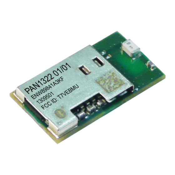
ENW89841A3KF Hardware Version Software Version Date Code YYWWDLL FCC ID:T7VEBMU FCC ID Machine readable 2D bar code Panasonic usage only, could be changed without any notice Case Figure 6 Package Marking Production Package Figure 7 Production Package All dimensions are in mm. -
Page 30: Pin Mark
PAN1322-SPP ENW89841A3KF Package Information 8.2.1 Pin Mark Pin 1 (A1) is marked on bottom footprint and on the top of the shield on the module according to Figure Diameter of pin 1 mark on the shield is 0.40mm. PAN1322 01/01... -
Page 31: Bluetooth Qualification And Regulatory Certification
PAN1322-SPP ENW89841A3KF Bluetooth Qualification and Regulatory Certification Bluetooth Qualification and Regulatory Certification Reference Design Figure 9 Reference Design Schematics User’s Manual Revision 1.3, 2013-08-14 Hardware Description... -
Page 32: Fcc Class B Digital Devices Regulatory Notice
There are no parts in ENW89841A3KF that can be modified by the user except modifications of the device BD data and loading of SW patches. Any changes or modifications made to this device that are not expressly approved by Panasonic, may void the user’s authority to operate the equipment. FCC Class B Digital Devices Regulatory Notice This equipment has been tested and found to comply with the limits for a Class B digital device, pursuant to Part 15 of the FCC Rules. -
Page 33: Fcc Interference Statement
PAN1322-SPP ENW89841A3KF Bluetooth Qualification and Regulatory Certification If possible place PAN1322 in the center of main PCB. min. 15mm min. 15mm 5.00 Restricted Area No copper any layer Top View PAN1322 All dimensions are in mm. Use a Ground plane in the area surrounding the PAN1322 module wherever possible. -
Page 34: Fcc Identifier
FCC ID: T7VEBMU European R&TTE Declaration of Conformity Hereby, Panasonic Industrial Devices Europe GmbH, declares that the Bluetooth module ENW89841A3KF is in compliance with the essential requirements and other relevant provisions of Directive 1999/5/EC. As a result of the conformity assessment procedure described in Annex III of the Directive 1999/5/EC, the end-... -
Page 35: Figure 12 Declaration Of Conformity
PAN1322-SPP ENW89841A3KF Bluetooth Qualification and Regulatory Certification Figure 12 Declaration of Conformity User’s Manual Revision 1.3, 2013-08-14 Hardware Description... -
Page 36: Bluetooth Qualified Design Id
Bluetooth Qualification and Regulatory Certification Bluetooth Qualified Design ID Panasonic has submitted End Product Listing (EPL) for PAN1322, based on Intel eBMU plattform, in the Qualified Product List of the Bluetooth SIG. These EPL are referring the Bluetooth qualfication of the SPP-AT application running on the eBMU chip under QD ID B021246. -
Page 37: Assembly Guidelines
10.1 General Description of the Module PAN1322-SPP is a Land Grid Array (LGA 8.7mm x 15.6mm) module made for surface mounting. The pad diameter is 0.6 mm and the pitch 1.2 mm. All solder joints on the module will reflow during soldering on the mother board. All components and shield will stay in place due to wetting force. -
Page 38: Figure 14 Cutout Drawing
PAN1322-SPP ENW89841A3KF Assembly Guidelines If possible place PAN1322 in the center of main PCB. min. 15mm min. 15mm 5.00 Restricted Area No copper any layer Top View PAN1322 All dimensions are in mm. Use a Ground plane in the area surrounding the PAN1322 module wherever possible. -
Page 39: Solder Paste Printing
PAN1322-SPP ENW89841A3KF Assembly Guidelines 10.3 Solder Paste Printing The solder paste deposited on the PCB by stencil printing has to be of eutectic or near eutectic tin leadfree / lead composition. A no-clean solder paste is preferred, since cleaning of the solder joints is difficult because of the small gap between the module and the PCB. -
Page 40: Package
PAN1322-SPP ENW89841A3KF Assembly Guidelines 10.4.3 Package PAN1322 is packed in tape on reel according to Figure Figure 16 Tape on Reel User’s Manual Revision 1.3, 2013-08-14 Hardware Description... -
Page 41: Soldering Profile
PAN1322-SPP ENW89841A3KF Assembly Guidelines 10.5 Soldering Profile Generally all standard reflow soldering processes (vapour phase, convection, infrared) and typical temperature profiles used for surface mount devices are suitable for the PAN1322 module. Wave soldering is not possible. Figure 17 Figure 18 shows example of a suitable solder reflow profile. -
Page 42: Rework
PAN1322-SPP ENW89841A3KF Assembly Guidelines At the reflow process each solder joint has to be exposed to temperatures above solder liquids for a sufficient time to get the optimum solder joint quality, whereas overheating the board with its components has to be avoided. -
Page 43: Alternative 2: Printing Solder
PAN1322-SPP ENW89841A3KF Assembly Guidelines 10.6.2.2 Alternative 2: Printing Solder To print solder on the module a fixture must be used. The purpose of the fixture is to get a flat surface and fix the stencil and module for printing. An example of how this fixture can be designed is shown in... -
Page 44: Voids In The Solder Joints
PAN1322-SPP ENW89841A3KF Assembly Guidelines 10.9 Voids in the Solder Joints 10.9.1 Expected Void Content and Reliability The content of voids is larger on LGA modules than for modules with BGA or leads. At a LGA solder joint the outgassing flux has a longer way to the surface of the solder and it has a relatively small surface to the air. - Page 45 PAN1322-SPP ENW89841A3KF Assembly Guidelines Stencil thickness A thick solder paste stencil means more surface area to the air and thereby easier for the outgassing flux to leave the solder. Temperature soldering profile Too short preheat time means that the flux does not get enough time to react and flux get entrapped in the solder and create voids.
-
Page 46: Terminology
PAN1322-SPP ENW89841A3KF Terminology Terminology Acknowledgement Asynchronous Connection-oriented (logical transport) Adaptive Frequency Hopping Adaptive Hop Sequence Automatic Repeat reQuest bit/bits (e.g. kb/s) Byte/Bytes (e.g. kB/s) BALUN BALanced UNbalanced BD_ADDR Bluetooth Device Address Bit Error Rate BlueMoon Universal Bill Of Material Bluetooth... - Page 47 PAN1322-SPP ENW89841A3KF Terminology Enhanced Data Rate EEPROM Electrically Erasable Programmable Read Only Memory eSCO Extended Synchronous Connection-Oriented (logical transport) Extended Voice (packet type) Forward Error Correction Frequency Hop Synchronization (packet) FIFO First In First Out (buffer) Frequency Modulation Firmware GFSK...
- Page 48 PAN1322-SPP ENW89841A3KF Terminology Least Significant Bit/Byte LT_ADDR Logical Transport Address Most Significant Bit/Byte MSRS Master-Slave Role Switch No Connection No OPeration Non-Volatile Memory Opcode Command Field Opcode Group Field Power Amplifier Printed Circuit Board Pulse Coded Modulation Protocol Data Unit...
- Page 49 PAN1322-SPP ENW89841A3KF Terminology To Be Determined Test Clock (JTAG signal) Test Data In (JTAG signal) Test Data Out (JTAG signal) Transport Layer Test Mode Select (JTAG signal) Transmit Transmit Data (UART signal) UART Universal Asynchronous Receiver & Transmitter ULPM Ultra Low Power Mode...
-
Page 50: References
Always the latest revision, as a pdf file, will be available under the link below (PAN1322 Application Note Design Guide) PAN1322-SPP User’s Manual (Data Sheet) It is this document. Always the latest revision, as a pdf file, will be available under the link below (PAN1322-SPP Data Sheet) User’s Manual... - Page 51 PAN1322-SPP ENW89841A3KF References User’s Manual Revision 1.3, 2013-08-14 Hardware Description...
- Page 52 . p i d e u . p a n a s o n i c . d e Published by Panasonic Industrial Devices Europe GmbH...