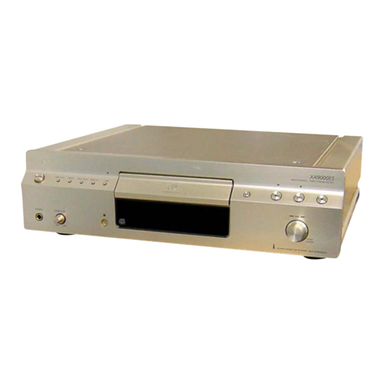
Sony SCD-XA9000ES Service Manual
Super audio cd player
Hide thumbs
Also See for SCD-XA9000ES:
- Operating instructions manual (68 pages) ,
- Specifications (2 pages) ,
- Limited warranty (1 page)
Table of Contents
Advertisement
SERVICE MANUAL
Ver. 1.4 2005.11
When a super audio CD is played
Playing frequency range 2 Hz to 100 kHz
Frequency response
2 Hz to 50 kHz (−3 dB)
Dynamic range
108 dB or more
Total harmonic distortion rate
0.0012 % or less
Wow and flutter
Value of measurable limit ( 0.001 %
W. PEAK) or less
When a CD is played
Frequency response
2 Hz to 20 kHz
Dynamic range
100 dB or more
Total harmonic distortion rate
0.0017 % or less
Wow and flutter
Value of measurable limit ( 0.001 %
W. PEAK) or less
Output connector
Jack type
Load impedance
Output level
Over 10 kilohms
ANALOG OUT
Phono
2 Vrms
jacks
(at 50 kilohms)
−18 dBm
Square
Light emitting
DIGITAL (CD)
(
optical
wave length:
OUT
660 nm
OPTICAL*
output
connector
Coaxial
0.5 Vp-p
75 ohms
DIGITAL (CD)
output
OUT
connector
COAXIAL*
Stereo
10 mW
32 ohms
PHONES
phone jack
*Output only the audio signals of the CD
Sony Corporation
9-961-151-05
2005K05-1
Home Audio Division
C 2005.11
Published by Sony Engineering Corporation
SCD-XA9000ES
Model Name Using Similar Mechanism NEW
CD Mechanism Type
Base Unit Name
Optical Pick-up Name
SPECIFICATIONS
i.LINK section
Pin
4 pins
Transmission speed
S200
(Maximum data transmission speed
200 Mbps)
Transmission protocol
A/M transmission protocol
Format (output)
Super Audio CD* (DSD PLAIN)
2 channel linear PCM (IEC 60958-3)
Sampling frequency: 44.1 kHz
* Conforms to the copy protection technology of DTLA (Revision
1.2).
General
Laser
Semiconductor laser
(SA-CD: λ = 650 nm)
(CD: λ = 780 nm)
Emission duration: continuous
Laser radiant power:
5.47 uW at 650 nm
*These output is the value measured at a distance of about
200mm from the objective lens surface on the optical pick-up.
Power requirements
Taiwan model:
110 V AC, 60 Hz
US, Canadian models:
120 V AC, 60 Hz
)
AEP model:
230 V AC, 50/60 Hz
Power consumption
32 W
430 × 127 × 387 mm
Dimensions (w/h/d)
(17 × 5 × 15
incl. projecting parts
Mass (approx.)
16.2 kg (35 lbs 12 oz.)
Canadian Model
CDM19JB-DVBU4C (Except AEP: Silver type)
CDM19JB-DVBU4D (AEP: Silver type)
DVBU4C (Except AEP: Silver type)
DVBU4D (AEP: Silver type)
KHM-230AAA
Supplied accessories
Audio connecting cord
phono jack × 2 (Red and White) y phono jack × 2 (Red
and White) (3)
phono jack × 1 (Black) y phono jack × 1 (Black) (2)
i.LINK connecting cord (1)
Remote commander RM-SX700 (1)
Size AA (R6) batteries (2)
AC power cord (1)
Plug adapter (1) (US, Canadian models only)
Design and specifications are subject to change without notice.
1
/
in.)
4
SUPER AUDIO CD PLAYER
US Model
AEP Model
E Model
Advertisement
Table of Contents

Related Manuals for Sony SCD-XA9000ES


Summary of Contents for Sony SCD-XA9000ES
-
Page 1: Specifications
10 mW 32 ohms PHONES Mass (approx.) 16.2 kg (35 lbs 12 oz.) phone jack *Output only the audio signals of the CD SUPER AUDIO CD PLAYER Sony Corporation 9-961-151-05 2005K05-1 Home Audio Division C 2005.11 Published by Sony Engineering Corporation... - Page 2 OPERATION. REPLACE THESE COMPONENTS WITH DE FONCTIONNEMENT. NE REMPLACER CES COM- SONY PARTS WHOSE PART NUMBERS APPEAR AS POSANTS QUE PAR DES PIÈCES SONY DONT LES SHOWN IN THIS MANUAL OR IN SUPPLEMENTS PUB- NUMÉROS SONT DONNÉS DANS CE MANUEL OU LISHED BY SONY.
-
Page 3: Table Of Contents
SCD-XA9000ES Ver. 1.3 TABLE OF CONTENTS SERVICING NOTES 5-37. Schematic Diagram – PANEL Section (2/2) – ....61 ..........4 5-38. Printed Wiring Board – A-POWER Board (Component Side) – ....... 62 GENERAL ..............10 5-39. Printed Wiring Boards – A-POWER (Conductor Side)/IC Boards – ....63 DISASSEMBLY 5-40. -
Page 4: Servicing Notes
SCD-XA9000ES Ver. 1.4 SECTION 1 SERVICING NOTES MODEL IDENTIFICATION (2) SACD (single layer) – Back Panel – Sled reverse move (sled in) Disc detect IC setting for SACD Servo error signal offset auto adjustment Spindle kick for LD on LD on Focus search Part No. - Page 5 SCD-XA9000ES Ver. 1.3 HOW TO OPEN THE DISC TABLE WHEN POWER SWITCH TURNS OFF loading panel assy 2 Draw out the loading panel assy in the direction of arrow B . cover (CAM) 1 Insert a tapering driver in the hole...
- Page 6 SCD-XA9000ES Note: Follow the disassembly procedure in the numerical order given. D-POWER/POWER BOARDS AND RF BOARD SERVICE POSITION 2 Turn over the set. 4 two bottom plates 3 eight screws (3 × 8) 3 four screws (3 × 8) – BOTTOM VIEW –...
- Page 7 SCD-XA9000ES MAIN BOARD SERVICE POSITION In checking the MAIN board, prepare jig (extension cable J-2501-205-A: 1.50 mm Pitch, 7 cores, Length 300 mm/ J-2501-086-A: 1.00 mm Pitch, 19 cores, Length 300 mm). Note: Be sure to ground the MAIN board with a lead wire when checking it.
- Page 8 SCD-XA9000ES AUDIO MODULE BLOCK SERVICE POSITION audio module block NOTE FOR INSTALLATION (AUDIO MODULE BLOCK) Note: When installing the audio module block, insert the audio module block as shown below. audio module block...
- Page 9 SCD-XA9000ES NOTE ON POSITION OF WIRE (FLAT TYPE) MAIN board wire (flat type) heatsink A-POWER board FRONT Heatsink gets heated up to a high temperature. Be careful to keep the position of wire (flat type).
-
Page 10: General
SCD-XA9000ES SECTION 2 This section is extracted from instruction manual. GENERAL Front Panel Parts Descriptions T ME/TEXT MENU MULTI/2CH SACD CD i.LINK POWER PHONES PHONE LEVEL PUSH EN ER 1 POWER switch 9 x button Press to turn on the player. -
Page 11: Rear Panel Parts Descriptions
SCD-XA9000ES Rear Panel Parts Descriptions CENTER 5.1CH OUT AC IN COAXIAL OPTICAL AUDIO OUT DIGITAL(CD) i.LINK S200 FRONT SURROUND SUB WOOFER 2CH OUT ANALOG 1 ANALOG 5.1CH OUT jacks Note Only the audio signals of the CD can be output from the Connect to an amplifier equipped with the 5.1CH... -
Page 12: Remote Parts Descriptions
SCD-XA9000ES Remote Parts Descriptions 1 CONTINUE button qs SACD/CD button Press to resume normal play from Shuffle Play or Each time you press the button, ”SACD“ or ”CD“ Program Play. appears in the display. Select the type of CD you want to play. -
Page 13: Disassembly
SCD-XA9000ES Ver. 1.3 SECTION 3 DISASSEMBLY • This set can be disassembled in the order shown below. 3-1. DISASSEMBLY FLOW Note 1: The process described in can be performed in any order. Note 2: Without completing the process described in , the next process can not be performed. -
Page 14: Case (Top), Side Plate
SCD-XA9000ES Note: Follow the disassembly procedure in the numerical order given. 3-2. CASE (TOP), SIDE PLATE 3 case (top) 2 two screws (flat head) 1 three screws (flat head) 7 two screws (3 × 8) 4 two screws (3 × 8) -
Page 15: Front Panel Section
SCD-XA9000ES 3-4. FRONT PANEL SECTION 5 two screws (3 × 8) 2 connector (CN706) 6 two brackets (F) 1 connector (CN453) 9 connector (CN994) 0 connector (CN601) 3 screw (BVTT 3 × 6) qa front panel section 4 harness 7 five screws (3 ×... -
Page 16: Rf Board, Mechanism Deck (Cdm19Jb-Dvbu4C Or Cdm19Jb-Dvbu4D)
SCD-XA9000ES Ver. 1.3 3-6. RF BOARD, MECHANISM DECK (CDM19JB-DVBU4C or CDM19JB-DVBU4D) CDM19JB-DVBU4C: Except AEP (Silver type) CDM19JB-DVBU4D: AEP (Sivler type) qs mechanism deck 2 two screws (CDM19JB-DVBU4C or CDM19JB-DVBU4D) (3 × 8) 4 two screws (3 × 8) 5 two screws (3 × 8) -
Page 17: Optical Pick-Up (Khm-230Aaa)
SCD-XA9000ES 3-8. OPTICAL PICK-UP (KHM-230AAA) 6 screw (BVTP2.6 × 8) 6 screw 7 stopper 1 two screws (BVTP2.6 × 8) (BVTT M3 S) 0 optical pick-up (KHM-230AAA) 9 insulator 7 stopper 6 screw (BVTP2.6 × 8) 9 insulator 7 stopper 2 holder (A. -
Page 18: Base Unit (Dvbu4C Or Dvbu4D)
SCD-XA9000ES Ver. 1.3 3-9. BASE UNIT (DVBU4C or DVBU4D) DVBU4C: Except AEP (Silver type) DVBU4D: AEP (Sivler type) 7 Insert a taper driver into the cover (CAM), and rotate in the arrow B direction to raise the base unit (DVBU4C or DVBU4D) in the arrow C direction. -
Page 19: Test Mode
SCD-XA9000ES SECTION 4 TEST MODE In this set, various checks are automatically performed by executing Setting Method of Test Mode [POWER] the commands in the test mode. Turn the button on while pressing the [MENU] [MENU] Note: This set makes adjustment every optical pick-up and stores its result dial and the button. - Page 20 SCD-XA9000ES TRACKING command (4X): Tracking servo related. Name Description Remarks TGAIN NM/UP The tracking servo gain is switched between normal and up Normal or up are switched alternately ADJ TRK DSP The traverse AGC and E-F balance adjustment is performed...
- Page 21 SCD-XA9000ES How to Apply Servo by Manual Operation Error display Causes (typical example) In analyzing failures of the set, the servo may be applied by manual EEPROM ERROR 1. IC903 (EEPROM) is faulty operation. To apply servo in the test mode, use the following SAMBA DRAM ERR 1.
- Page 22 SCD-XA9000ES 4-3. SET CHECK (AUTOMATIC VARIOUS MEASUREMENTS) The operational stability of the set is checked. The check and OK/NG judgment are performed automatically. Note: In the set check using the CD, besides a checking, the MIRR time used for the disc check is measured every optical pick-up, and from the measured result, the threshold value is calculated and it is stored in the EEPROM (IC903) on the MAIN board.
- Page 23 SCD-XA9000ES Specified Value: Specified value used for OK/NG judgment when executing 92. SET CHECKtAUTO CHECK SP? Measured Items Specified value RF AVRG (ADJ) 8Ch to ABh VC AVRG (ADJ) 1F7h to09h (1) CD 1EEh to 12h FE AVRG (ADJ) (2) SACD...
- Page 24 SCD-XA9000ES 4-4. SACD (DL) DISC OPERATION CHECK 4-6. WAVEFORMS CHECK (• Perform as necessary) BU Electrical Adjustment Mode This checking performs the focus jump using a DL disc, which is The BU electrical adjustment mode is used to check the S curve a dual-layer HD disc, to verify the stability of the set.
- Page 25 SCD-XA9000ES Ver 1.1 Traverse Check RF Level Check CLV Jitter Check (CD only) 4-7. i.LINK SIGNAL OPERATION CHECK Connection: Connection: Connection: Connect the set to a unit equipped with the i.LINK terminal to oscilloscope oscilloscop e check if the bus reset occurs correctly. By this operation, a loose oscilloscope connection of the connector or a disconnection of the i.LINK cable...
-
Page 26: Diagrams
SCD-XA9000ES SECTION 5 DIAGRAMS 5-1. BLOCK DIAGRAM – RF/SERVO Section – • Signal Path : SACD PLAY OPTICAL PICK-UP BLOCK : CD PLAY (ANALOG OUT) (KHM-230AAA) : CD PLAY (DIGITAL OUT) RFSIN ATOP RFAC RFAC DVDRFP ATON (Page 27) DOUT... -
Page 27: Block Diagram - Main Section (1/2)
SCD-XA9000ES 5-2. BLOCK DIAGRAM – MAIN Section (1/2) – D+5V CENTER VOLTAGE DRVC +2.5V GENERATOR IC503 SDATAL 83 DLI DSAL SDATAR (Page 29) DSAR WARFI SDATAC DSAC SDATASW DSASW DLFEI DLFEO RFAC (Page 26) RFIN SDATALS DSALS DLSI DLSO SDATARS... -
Page 28: Block Diagram - Main Section (2/2)
SCD-XA9000ES 5-3. BLOCK DIAGRAM – MAIN Section (2/2) – D0 – D7 (Page 27) DATA BUS DATA BUS A0 – A7 ADDRESS BUS ADDRESS BUS (Page 27) XHRD, XHWR, XCS1882, XINIT0, XINIT1, XRST_DVD (Page 27) 14 – 21 89 – 96 D0 –... -
Page 29: Block Diagram - Audio Section (1/2)
SCD-XA9000ES 5-4. BLOCK DIAGRAM – AUDIO Section (1/2) – (Page 27) DIGITAL FILTER, DATA SELECTOR CURRENT PULSE, IC305 D/A CONVERTER DATA SELECTOR IC101 IC307 SDATAL FL– SDATALS (Page 30) LOUTL+ 5 DATA SDATAL LOUTR+ SDATAC LOUTL– LRCK/G 4 LRCK LOUTR–... -
Page 30: Block Diagram - Audio Section (2/2)
SCD-XA9000ES 5-5. BLOCK DIAGRAM – AUDIO Section (2/2) – • Signal Path : SACD PLAY FL– AUDIO FILTER, I-V CONVERTER LINE AMP IC102 (Page 29) IC103 J301 FRONT FR – AUDIO FILTER, I-V CONVERTER LINE AMP IC202 IC203 CDTL/ RY152... -
Page 31: Block Diagram - Link Section
SCD-XA9000ES 5-6. BLOCK DIAGRAM – LINK Section – J1901 i. LINK S200 AUDIO OUT DOUT • Signal Path (Page 26) IEC958 TPA0P TA0P : CD PLAY (DIGITAL OUT) TPA0N TA0N TPB0P TB0P TPB0N TB0N TPBIAS0 BIAS IOUT0 – IOUT5 (Page 27) DATA BUS D0 –... -
Page 32: Block Diagram - Panel/Power Supply Section
SCD-XA9000ES 5-7. BLOCK DIAGRAM – PANEL/POWER SUPPLY Section – T902 POWER TRANSFORMER (FOR DIGITAL) FL. DATA SOUT FL. CLK (Page 28) S990 J491 XFBSY POWER AC IN XIFCS XFRRST RESET –31V REGULATOR RECT LINE FILTER SEGMENT DRIVE FL –31V FL801 Q451 D451 –... -
Page 33: Note For Printed Wiring Boards And Schematic Diagrams
SCD-XA9000ES Ver. 1.3 5-8. NOTE FOR PRINTED WIRING BOARDS AND SCHEMATIC DIAGRAMS • Circuit Boards Location Note on Printed Wiring Board: Note on Schematic Diagram: • All capacitors are in µF unless otherwise noted. pF: µµF • X : parts extracted from the component side. -
Page 34: Printed Wiring Boards - Servo Section
SCD-XA9000ES Ver. 1.3 5-9. PRINTED WIRING BOARDS – SERVO Section – • :Uses unleaded solder. See page 33 for Circuit Boards Location. IC081 IC001 IC004 MAIN BOARD CN708 (Page 36) SWITCH BOARD LOADING MOTOR BOARD S002 CN001 C001 (LOADING OUT) -
Page 35: Schematic Diagram - Servo Section
SCD-XA9000ES Ver. 1.3 5-10. SCHEMATIC DIAGRAM – SERVO Section – • • See page 65 for Waveforms. See page 70 for IC Block Diagram. (AEP: SILVER) MAIN BOARD (1/7) CN708 (Page CXD1881AR 2 The components identified by mark 0 or dotted Les composants identifiés par une marque 0 sont... -
Page 36: Main Board (Component Side)
SCD-XA9000ES 5-11. PRINTED WIRING BOARD – MAIN Board (Component Side) – • See page 33 for Circuit Boards Location. :Uses unleaded solder. • Semiconductor Location Ref. No. Location D-POWER A-POWER LINK BOARD LINK BOARD RF BOARD IC504 MAIN BOARD BOARD... -
Page 37: Printed Wiring Board - Main Board (Conductor Side)
SCD-XA9000ES 5-12. PRINTED WIRING BOARD – MAIN Board (Conductor Side) – • See page 33 for Circuit Boards Location. :Uses unleaded solder. • Semiconductor Location Ref. No. Location D903 D904 MAIN BOARD (CONDUCTOR SIDE) D905 IC502 IC503 IC512 C517 C591... -
Page 38: Schematic Diagram - Main Board (1/7)
SCD-XA9000ES 5-13. SCHEMATIC DIAGRAM – MAIN Board (1/7) – • • See page 65 for Waveforms. See page 70 for IC Block Diagram. (1/7) CN703 FL750 FB700 FB701 DGND C790 (Page 57) FL751 FB703 FB704 CN707 C791 D+3.3V 6.3V MOT+12V... -
Page 39: Schematic Diagram - Main Board (2/7)
SCD-XA9000ES 5-14. SCHEMATIC DIAGRAM – MAIN Board (2/7) – • See page 65 for Waveform. • See page 70 for IC Block Diagram. (Page 38) (2/7) (Page 44) R545 100k R701 (1/2) 220k C523 0.0015 R703 R704 R544 IC703(2/2) R725... -
Page 40: Schematic Diagram - Main Board (3/7)
SCD-XA9000ES 5-15. SCHEMATIC DIAGRAM – MAIN Board (3/7) – (Page 38) (3/7) (Page 39) +5V REGULATOR IC504 µPC2905T-E1 C528 C520 C526 C525 R512 C519 R632 R606 C587 C502 R554 3.3k C536 R534 0.47 3.3k C527 R642 560p C562 FOCUS/TRACKING COIL DRIVE,... -
Page 41: Schematic Diagram - Main Board (4/7)
SCD-XA9000ES 5-16. SCHEMATIC DIAGRAM – MAIN Board (4/7) – • See page 65 for Waveforms. (4/7) C871 R870 C865 C867 C866 FL813 FB717 0.01 0.01 0.01 0.01 C809 C800 C941 +2.5V REGULATOR 0.01 IC702 TA48M025F C841 C815 C848 C804 FL812 FB718 0.01... -
Page 42: Schematic Diagram - Main Board (5/7)
SCD-XA9000ES 5-17. SCHEMATIC DIAGRAM – MAIN Board (5/7) – • See page 65 for Waveforms. (5/7) CN710 DGND C845 FB722 C844 FL809 MLS_OSC R1054 MLS_OSC (OSC) MLS_RST R1055 MLS_RST (RST) MLS_SCK R1056 MLS_SCK (SCL) C821 0.01 DGND MLS_SIO R1057 MLS_SIO... -
Page 43: Schematic Diagram - Main Board (6/7)
SCD-XA9000ES 5-18. SCHEMATIC DIAGRAM – MAIN Board (6/7) – • See page 65 for Waveforms. • See page 70 for IC Block Diagrams. (Page 41) (Page 42) (6/7) SPC970_BUS PARA_BUS (Page 39) ANALOG_BUS FL901 FB721 C901 C902 R912 R913 C906 0.01... -
Page 44: Schematic Diagram - Main Board (7/7)
SCD-XA9000ES 5-19. SCHEMATIC DIAGRAM – MAIN Board (7/7) – (Page 41) (Page 42) (7/7) (Page 39) R999 R935 FL904 C911 DIGITAL OUT C917 R1000 C918 R933 R997 ON/OFF SWITCH IC810 SN74AHC1G08DCKR CN704 R857 FB724 FL906 FB725 3.3VD C914 C940 C913... -
Page 45: Printed Wiring Board - D-Out Board
SCD-XA9000ES 5-20. PRINTED WIRING BOARD – D-OUT Board – • 5-21. SCHEMATIC DIAGRAM – D-OUT Board – See page 33 for Circuit Boards Location. :Uses unleaded solder. D-OUT BOARD D-OUT BOARD (COMPONENT SIDE) (CONDUCTOR SIDE) C448 IC442 C442 R442 T441... -
Page 46: Mother Board (Component Side)
SCD-XA9000ES 5-22. PRINTED WIRING BOARD – MOTHER Board (Component Side) – • :Uses unleaded solder. See page 33 for Circuit Boards Location. MOTHER BOARD (COMPONENT SIDE) (21) 1-682-045-... -
Page 47: Printed Wiring Board - Mother Board (Conductor Side)
SCD-XA9000ES 5-23. PRINTED WIRING BOARD – MOTHER Board (Conductor Side) – • :Uses unleaded solder. See page 33 for Circuit Boards Location. (Page 54) (Page 63) (Page 63) (Page 54) (Page 36) (Page 36) AUDIO C/SW BOARD A-POWER BOARD A-POWER BOARD... -
Page 48: Schematic Diagram - Mother Board (1/2)
SCD-XA9000ES 5-24. SCHEMATIC DIAGRAM – MOTHER Board (1/2) – • See page 70 for Waveforms. • See page 70 for IC Block Diagrams. (1/2) CN303 R303 C307 COUNTER IC303 C308 SN74LV161APWR (Page 64) L301 CN302 CARRY R304 DFGND CLOCK BUFFER... -
Page 49: Schematic Diagram - Mother Board (2/2)
SCD-XA9000ES 5-25. SCHEMATIC DIAGRAM – MOTHER Board (2/2) – (2/2) CN351 -12V +12V -12V +12V D354 C384 RY353 -12V 1SS352-TPH3 R351 C353 +12V R354 (Page 64) 6.8k C362 -12V 160V R352 C360 C361 +12V R353 R355 CN352 R360 C373 Q394,395 IC351 3.3k... -
Page 50: Printed Wiring Board - Audio Front Board
SCD-XA9000ES 5-26. PRINTED WIRING BOARD – AUDIO FRONT Board – • See page 33 for Circuit Boards Location. :Uses unleaded solder. • Semiconductor Location Ref. No. Location AUDIO FRONT BOARD (COMPONENT SIDE) D152 D154 D155 IC101 IC102 IC103 IC151 IC201... -
Page 51: Schematic Diagram - Audio Front Board
SCD-XA9000ES 5-27. SCHEMATIC DIAGRAM – AUDIO FRONT Board – • See page 70 for IC Block Diagrams. FR153 D155 1SS367-T3 Q153 RN2405-TE85L D152 RELAY UDZS-TE-17 +3.3V REGULATOR -9.1B DRIVE IC151 NJM2370U33-TE2 R160 Q154 DTC114EKA-T146 FR152 RELAY C152 C162 C151 C165... -
Page 52: Printed Wiring Board - Audio Surr Board
SCD-XA9000ES 5-28. PRINTED WIRING BOARD – AUDIO SURR Board – • See page 33 for Circuit Boards Location. :Uses unleaded solder. • Semiconductor Location Ref. No. Location AUDIO SURR BOARD (COMPONENT SIDE) D1151 D1152 D1153 D1154 D1155 IC1101 IC1102 IC1103... -
Page 53: Schematic Diagram - Audio Surr Board
SCD-XA9000ES 5-29. SCHEMATIC DIAGRAM – AUDIO SURR Board – • See page 70 for IC Block Diagrams. FR1153 Q1151 Q1153 RN2405-TE85L RN2405-TE85L D1155 D1151 D1152 RELAY RELAY 1SS367-T3 UDZS-TE-17 UDZS-TE-17 -9.1B DRIVE -9.1B DRIVE +3.3V REGULATOR IC1151 R1180 R1159 FR1151... -
Page 54: Printed Wiring Board - Audio C/Sw Board
SCD-XA9000ES 5-30. PRINTED WIRING BOARD – AUDIO C/SW Board – • See page 33 for Circuit Boards Location. :Uses unleaded solder. • Semiconductor Location Ref. No. Location AUDIO C/SW BOARD (COMPONENT SIDE) D2151 D2152 D2153 D2154 D2155 D2156 D2157 IC2101... -
Page 55: Schematic Diagram - Audio C/Sw Board
SCD-XA9000ES 5-31. SCHEMATIC DIAGRAM – AUDIO C/SW Board – • See page 70 for IC Block Diagrams. FR2153 Q2151 Q2155 Q2153 RN2405-TE85L RN2405-TE85L D2151 RN2405-TE85L D2152 D2157 D2155 UDZS-TE-17 RELAY RELAY UDZS-TE-17 RELAY UDZS-TE-17 1SS367-T3 -9.1B DRIVE -9.1B -9.1B DRIVE... -
Page 56: Schematic Diagram - Link Board (1/2)
SCD-XA9000ES Ver. 1.4 5-32. SCHEMATIC DIAGRAM – LINK Board (1/2) – • See page 70 for Waveforms. (1/2) C1960 X1903 C1961 20MHz R1806 4.7k Q1903 R1803 C1944 R1897 2SC3624A-T1L15 4.7k OSC ON/OFF SWITCH R1899 R1997 C1938 R1935 R1938 C1933 R1939... -
Page 57: Schematic Diagram - Link Board (2/2)
SCD-XA9000ES 5-33. SCHEMATIC DIAGRAM – LINK Board (2/2) – (Page 56) (2/2) FL1901 FL1904 FB1905 CN1902 R1804 C1959 4.7k R1990 C1922 C1953 DGND R1801 C1901 C1902 C1907 C1908 (Page 38) X1901 R1909 Q1901 24.576MHz 4.7k 2SC3624A-T1L15 OSC ON/OFF R1908 100k... -
Page 58: Printed Wiring Board - Link Board
SCD-XA9000ES Ver. 1.4 5-34. PRINTED WIRING BOARD – LINK Board – • See page 33 for Circuit Boards Location. :Uses unleaded solder. • Semiconductor Location Ref. No. Location J1901 D1901 i. LINK S200 AUDIO OUT D1903 2 3 4 LINK BOARD... -
Page 59: Printed Wiring Boards - Panel Section
SCD-XA9000ES 5-35. PRINTED WIRING BOARDS – PANEL Section – • :Uses unleaded solder. See page 33 for Circuit Boards Location. DISPLAY BOARD MAIN BOARD CN706 D-POWER BOARD (Page 36) CN453 (Page 66) D805 CN811 FL801 FLUORESCENT INDICATOR TUBE R844 CN801... -
Page 60: Schematic Diagram - Panel Section (1/2)
SCD-XA9000ES 5-36. SCHEMATIC DIAGRAM – PANEL Section (1/2) – • See page 70 for Waveforms. FL801 FLUORESCENT INDICATOR TUBE CN801 R846 R845 R844 R843 SOUT R842 Q803 Q802 Q801 RESET DTC114EKA DTC114EKA DTC114EKA (Page 44) SEGMENT GRID GRID DRIVE R806... -
Page 61: Schematic Diagram - Panel Section (2/2)
SCD-XA9000ES 5-37. SCHEMATIC DIAGRAM – PANEL Section (2/2) – R861 R862 RV601 1k/1k CN601 PHONE D801 D802 L605 L608 SEL5521C-TP15 SEL5821A-TP15 LEVEL 3.3µH L601 L606 L609 3.3µH L602 J601 PHONES (Page 49) L607 L610 3.3µH L603 CN804 LED(PLAY) LED(PAUSE) C603... -
Page 62: Printed Wiring Board - A-Power Board (Component Side)
SCD-XA9000ES 5-38. PRINTED WIRING BOARD – A-POWER Board (Component Side) – • See page 33 for Circuit Boards Location. :Uses unleaded solder. A-POWER BOARD (COMPONENT SIDE) (21) 1-682-046-... -
Page 63: Printed Wiring Boards - A-Power (Conductor Side)/Ic Boards
SCD-XA9000ES 5-39. PRINTED WIRING BOARDS – A-POWER (Conductor Side)/IC Boards – • See page 33 for Circuit Boards Location. :Uses unleaded solder. • Semiconductor Location Ref. No. Location MAIN BOARD D-POWER BOARD D401 CN707 CN456 D402 (Page 36) A-POWER BOARD... -
Page 64: Schematic Diagram - A-Power/Ic Boards
SCD-XA9000ES 5-40. SCHEMATIC DIAGRAM – A-POWER/IC Boards – CN455 IC452 BA05T D459 CN452 D5-GND EC10QS04-TE12L5 L457 D+5V D460 EC10QS04-TE12L5 THP452 (Page 67) D461 EC10QS04-TE12L5 C465 C464 +5V REGULATOR C468 C466 D462 THP453 R457 2200 6800 (Page 69) EC10QS04-TE12L5 L458 +5V REGULATOR CN454 D+3.3V... - Page 65 SCD-XA9000ES • Waveforms – RF Board – 1 IC001 el (TE) (CD Play) 5 IC001 tj (RFAC) (CD Play) qd IC509 ra (TE) (CD Play) qk IC509 yj (BCK) (CD Play) wd IC802 i; (PHRI) ea IC901 ra (EXTAL) Approx.
-
Page 66: Printed Wiring Board - D-Power Board
SCD-XA9000ES 5-41. PRINTED WIRING BOARD – D-POWER Board – • :Uses unleaded solder. See page 33 for Circuit Boards Location. • Semiconductor Location Ref. No. Location D421 D-POWER BOARD (COMPONENT SIDE) D-POWER BOARD (CONDUCTOR SIDE) D422 D423 D451 D452 D453... -
Page 67: Schematic Diagram - D-Power Board
SCD-XA9000ES 5-42. SCHEMATIC DIAGRAM – D-POWER Board – L451 C452 C451 0.022 0.022 100V 100V L452 FR451 D451 EC10DS2 L453 Q451 D452 2SA1213O EC10DS2 D422 C457 C455 C454 C453 R455 R454 C458 R452 R462 R451 UDZSTE- -31V 0.022 0.022 220k CN453 173.9B... -
Page 68: Printed Wiring Boards - Ac/Ac Sw Boards
SCD-XA9000ES 5-43. PRINTED WIRING BOARDS – AC/AC SW Boards – • See page 33 for Circuit Boards Location. :Uses unleaded solder. AC BOARD AC BOARD (COMPONENT SIDE) (CONDUCTOR SIDE) (CHASSIS) ETP401 J491 AC IN CN493 T491 T492 T901 POWER TRANSFORMER... -
Page 69: Schematic Diagram - Ac/Ac Sw Boards
SCD-XA9000ES 5-44. SCHEMATIC DIAGRAM – AC/AC SW Boards – T901 POWER TRANSFORMER (FOR AUDIO) S481 POWER CN491 CN493 CN994 T491 (Page 64) C494 10000p C996 250V 10000p 250V (Page 64) J491 T902 ~AC IN POWER C492 C491 TRANSFORMER 10000p 10000p... - Page 70 SCD-XA9000ES • Waveforms • IC Block Diagrams – MOTHER Board – – LINK Board – – DISPLAY Board – – RF Board – qj IC303 qf (QA) ra IC1903 qd (XOUT) ta IC801 t; (OSCO) IC001 CXD1881AR-2 64 63 62 61 60 59...
- Page 71 SCD-XA9000ES – MAIN Board – IC509 CXD3068Q 59 58 57 56 55 54 53 52 51 50 49 48 47 46 45 44 43 42 41 DVDD2 ASYE DIGITAL ASYMMETRY CORRECTOR DIGITAL DOUT LRCK D/A DIGITAL PCMD INTERFACE DEMODULATOR TES1...
- Page 72 SCD-XA9000ES IC701 TMC57929PGF-RDP 132131130129128 126125 123122 121120 119118 117116115114113112111110109108107 106105104103102101100 99 98 97 96 95 94 93 92 91 90 89 RF ASYMMETRY GNDA2 CONTROLLER MAIN DATA ECC & EDC PRIORITY RESOLVE GNDA1 & SEQUENSOR XRAS CD-ROM MDIN2 MAIN DATA MDIN1 ECC &...
- Page 73 SCD-XA9000ES IC902 TC7WH157FU (TE12R) IC905 M51957BFP-600C SELECT EN G – GND 4 – MOTHER Board – IC303 HD74LV161ATELL IC304, 305, 306, 307, 308 SN74LV157APWR SELECT 1 1A 2 STROBE INPUT RIPPLE ENABLE INPUT CARRY OUTPUT OUTPUT 1 1 2 OUTPUT...
-
Page 74: Ic Pin Function Description
SCD-XA9000ES 5-45. IC PIN FUNCTION DESCRIPTION • MAIN BOARD IC509 CXD3068Q (DIGITAL SERVO PROCESSOR, DIGITAL SIGNAL PROCESSOR, DIGITAL FILTER) Pin No. Pin Name Description DVDD0 — Power supply terminal (+3.3V) (digital system) XRST Reset signal input from the I/O expander “L”: reset... - Page 75 SCD-XA9000ES Pin No. Pin Name Description IGEN Stabilized current input for operational amplifiers AVDD0 — Power supply terminal (+3.3V) (analog system) ASYO EFM full-swing output terminal ASYI Asymmetry comparator voltage input terminal RFAC EFM signal input from the SACD/CD RF amplifier AVSS1 —...
- Page 76 SCD-XA9000ES • MAIN BOARD IC701 TMC57929PGF-RDP (SACD DECODER) Pin No. Pin Name Description 1, 2 D5, D6 Two-way data bus with the CPU and I/O expander — Ground terminal (digital system) Two-way data bus with the CPU and I/O expander Address signal input from the CPU —...
- Page 77 SCD-XA9000ES Pin No. Pin Name Description HINT Not used XS16 Not used Not used XPDI Not used VDDS — Power supply terminal (+5V) (digital system) 59, 60 HA0, HA2 Not used — Ground terminal (digital system) 62, 63 HCS0, HCS1 Not used —...
- Page 78 SCD-XA9000ES Pin No. Pin Name Description VCOR1 — VCO oscillating range setting resistor connected terminal VCOIN VCO input terminal 122, 123 GNDA4, GNDA3 — Ground terminal (analog system) LPF5 Signal output from the operation amplifier from PLL loop filter Middle point voltage (+1.65V) input terminal...
- Page 79 SCD-XA9000ES Pin No. Pin Name Description — Power supply terminal (+3.3V) (digital system) 172 to 176 D0 to D4 Two-way data bus with the CPU and I/O expander...
- Page 80 SCD-XA9000ES • MAIN BOARD IC801 CXD2753R (DSD DECODER) Pin No. Pin Name Description VSCA0 — Ground terminal (for core) XMSLAT Serial data latch pulse signal input from the CPU MSCK Serial data transfer clock signal input from the CPU MSDATI...
- Page 81 SCD-XA9000ES Pin No. Pin Name Description BCKAO Bit clock signal (2.8224 MHz) output terminal for DSD data output Not used PHREFI Clock signal (2.8224 MHz) input terminal PHREFO Phase reference signal output terminal for DSD output phase modulation Not used...
- Page 82 SCD-XA9000ES Pin No. Pin Name Description WRFD Not used Operation clock signal input for PSP physical disc mark detection from the SACD decoder WAVDD0, 124, 125 — A/D power supply terminal (+2.5V) (for PSP physical disc mark detection) WAVDD1 WARFI...
- Page 83 SCD-XA9000ES • MAIN BOARD IC802 CXD9722TQ (DSD DIGITAL SIGNAL PROCESSOR) Pin No. Pin Name Description 1 to 5 D1 to D5 Two-way data bus with the SD-RAM — Power supply terminal (+3.3V) 7, 8 D6, D7 Two-way data bus with the SD-RAM —...
- Page 84 SCD-XA9000ES Pin No. Pin Name Description — Power supply terminal (+3.3V) — Ground terminal DLDRI Analog audio data input terminal Not used CSWI Center and sub woofer audio data input terminal Not used SLSRI Surround audio data input terminal Not used...
- Page 85 SCD-XA9000ES • MAIN BOARD IC901 CXP973064-241R (CPU) Pin No. Pin Name Description MUTE_ LOAD Muting on/off control signal output to the loading motor drive “L”: muting on RST_DY Reset signal output to the DSD digital signal processor “L”: reset Digital out on/off control signal output to the digital signal processor DOCTRL “L”: digital out off, “H”: digital out on...
- Page 86 SCD-XA9000ES Pin No. Pin Name Description BUSY_DP Busy signal input from the display controller SIN_DP Serial data input from the display controller SOUT_DP Serial data output to the display controller SCLK_DP Serial data transfer clock signal output to the display controller —...
- Page 87 SCD-XA9000ES • MAIN BOARD IC904 ISPLSI2032VE-110LT44-SA8 (I/O EXPANDER) Pin No. Description Pin Name Serial data selection signal output for SIN_DSD (rk pin of CPU) SI_SEL “L”: DSD decoder serial data, “H”: DSD digital signal processor serial data ZEROL L-ch zero data flag detection signal input terminal Not used FS64 Clock signal (2.8224 MHz) output terminal Not used...
- Page 88 SCD-XA9000ES • LINK BOARD IC1902 TMS320VC5409PGE100A (I-LINK DSP) Pin No. Pin Name Description — Ground terminal Address signal output terminal Not used — Ground terminal DVDD (3.3V) — Power supply terminal (+3.3V) Address signal output terminal Not used Two-way data bus with the i-link system controller...
- Page 89 SCD-XA9000ES Pin No. Pin Name Description HRDY Ready signal output to the i-link system controller DVDD (3.3V) — Power supply terminal (+3.3V) — Ground terminal Two-way data bus with the i-link system controller 59, 60 BDX0, BDX2 Serial data output terminal Not used...
- Page 90 SCD-XA9000ES Pin No. Pin Name Description 113 to 119 D6 to D12 Two-way data bus terminal Not used Two-way data bus with the i-link system controller 121 to 123 D13 to D15 Two-way data bus terminal Not used Two-way data bus with the i-link system controller CVDD (1.8V)
- Page 91 SCD-XA9000ES • LINK BOARD IC1903 M30626FHPFP-SCD-XA9000 (I-LINK SYSTEM CONTROLLER) Pin No. Pin Name Description 1 to 7 HD6 to HD0 Two-way data bus with the i-link DSP External data bus line byte selection signal input terminal BYTE “L”: 16 bit, “H”: 8 bit Fixed at “L” in this set CNVSS —...
- Page 92 SCD-XA9000ES Pin No. Pin Name Description — Ground terminal 65 to 71 A7 to A1 Address signal output to the i-link interface and EEPROM Address signal output terminal Not used 73 to 88 D15 to D0 Two-way data bus with the i-link interface and EEPROM...
- Page 93 SCD-XA9000ES • DISPLAY BOARD IC803 CXP84120-092Q (DISPLAY CONTROLLER) Pin No. Pin Name Description 1 to 29 Not used RESET Reset signal input from the I/O expander “L”: reset EXTAL System clock output terminal (8 MHz) XTAL System clock input terminal (8 MHz) —...
-
Page 94: Exploded Views
SCD-XA9000ES Ver. 1.3 SECTION 6 EXPLODED VIEWS NOTE: • -XX and -X mean standardized parts, so they • Items marked “*” are not stocked since they The components identified by mark 0 or dotted line with mark 0 are may have some difference from the original are seldom required for routine service. -
Page 95: Front Panel Section-1
SCD-XA9000ES Ver 1.2 6-2. FRONT PANEL SECTION-1 not supplied not supplied not supplied supplied not supplied supplied supplied with J601 not supplied supplied with RV601 not supplied front panel section-2 Ref. No. Part No. Description Remark Ref. No. Part No. -
Page 96: Front Panel Section-2
SCD-XA9000ES Ver. 1.3 6-3. FRONT PANEL SECTION-2 not supplied supplied supplied Ref. No. Part No. Description Remark Ref. No. Part No. Description Remark 4-246-560-22 PANEL, FRONT (BLACK) 4-975-105-01 WINDOW, RAY CATCHER (BLACK) 4-246-560-32 PANEL, FRONT (GOLD) 4-975-105-32 WINDOW, RAY CATCHER (GOLD) -
Page 97: Bottom Section
SCD-XA9000ES 6-4. BOTTOM SECTION board section-1 supplied not supplied not supplied Ref. No. Part No. Description Remark Ref. No. Part No. Description Remark 4-970-124-12 CUSHION (F50180S) 4-929-074-01 SCREW (3X8) 4-970-487-01 FOOT (F50180S) 3-531-576-01 RIVET (AEP) 4-970-488-01 SPACER (F50180S) 7-685-886-09 SCREW +BVTT 4X20 (S) -
Page 98: Board Section-1
SCD-XA9000ES Ver. 1.4 6-5. BOARD SECTION-1 not supplied supplied supplied CDM19JB-DVBU4C supplied board section-2 Ref. No. Part No. Description Remark Ref. No. Part No. Description Remark 4-929-074-01 SCREW (3X8) A-4747-600-A A-POWER BOARD, COMPLETE (EXCEPT AEP) 1-860-271-21 IC BOARD X-4954-269-1 SCREW ASSY, + BVTT... -
Page 99: Board Section-2
SCD-XA9000ES Ver 1.2 6-6. BOARD SECTION-2 not supplied T901 T902 not supplied supplied not supplied supplied Canadian supplied not supplied supplied supplied not supplied chassis section The components identified by Les composants identifiés par une mark 0 or dotted line with marque 0 sont critiques pour la mark 0 are critical for safety. -
Page 100: Chassis Section
SCD-XA9000ES 6-7. CHASSIS SECTION not supplied not supplied not supplied not supplied supplied not supplied supplied not supplied not supplied Ref. No. Part No. Description Remark Ref. No. Part No. Description Remark 4-929-074-01 SCREW (3X8) 3-655-653-01 BAND (TAITON), BINDING * 302... -
Page 101: Mechanism Deck Section
SCD-XA9000ES Ver. 1.3 6-8. MECHANISM DECK SECTION CDM19JB-DVBU4C: Except AEP (Silver type) CDM19JB-DVBU4D: AEP (Silver type) not supplied not supplied not supplied not supplied not supplied DVBU4C not supplied not supplied not supplied not supplied Ref. No. Part No. Description Remark Ref. -
Page 102: Base Unit Section
SCD-XA9000ES Ver. 1.3 6-9. BASE UNIT SECTION DVBU4C: Except AEP (Silver type) DVBU4D: AEP (Siver type) not supplied not supplied not supplied not supplied The components identified by Les composants identifiés par une mark 0 or dotted line with marque 0 sont critiques pour la mark 0 are critical for safety. -
Page 103: Electrical Parts List
SCD-XA9000ES Ver 1.2 SECTION 7 ELECTRICAL PARTS LIST AC SW A-POWER NOTE: • Due to standardization, replacements in the • Items marked “*” are not stocked since they The components identified by 0 or dotted line with mark mark parts list may be different from the parts speci- are seldom required for routine service. - Page 104 SCD-XA9000ES Ver 1.2 A-POWER AUDIO C/SW Ref. No. Part No. Description Remark Ref. No. Part No. Description Remark < DIODE > R402 1-259-991-11 CARBON MELF 1/8W R403 1-259-991-11 CARBON MELF 1/8W D401 8-719-079-01 DIODE FRH10A15 R404 1-259-979-11 CARBON MELF 1/8W...
- Page 105 SCD-XA9000ES AUDIO C/SW Ref. No. Part No. Description Remark Ref. No. Part No. Description Remark IC2201 8-759-836-44 IC CXD9657N/2K C2162 1-119-800-11 ELECT 100uF C2163 1-165-319-11 CERAMIC CHIP 0.1uF IC2202 8-759-566-39 IC OPA2132UA/2K5 C2164 1-165-319-11 CERAMIC CHIP 0.1uF IC2203 8-759-566-39 IC OPA2132UA/2K5...
- Page 106 SCD-XA9000ES AUDIO C/SW AUDIO FRONT Ref. No. Part No. Description Remark Ref. No. Part No. Description Remark R2201 1-259-937-11 CARBON MELF 1/8W C160 1-165-319-11 CERAMIC CHIP 0.1uF R2203 1-259-979-11 CARBON MELF 1/8W C162 1-119-800-11 ELECT 100uF R2204 1-259-979-11 CARBON MELF...
- Page 107 SCD-XA9000ES AUDIO FRONT AUDIO SURR Ref. No. Part No. Description Remark Ref. No. Part No. Description Remark < COIL > R218 1-260-028-11 CARBON MELF 470K 1/8W R219 1-259-971-11 CARBON MELF 1/8W L102 1-408-619-31 MICRO INDUCTOR 220uH L202 1-408-619-31 MICRO INDUCTOR...
- Page 108 SCD-XA9000ES AUDIO SURR Ref. No. Part No. Description Remark Ref. No. Part No. Description Remark C1211 1-136-819-11 FILM 0.0068uF 5% 100V R1103 1-259-979-11 CARBON MELF 1/8W C1212 1-136-817-11 FILM 0.0033uF 5% 100V R1104 1-259-979-11 CARBON MELF 1/8W C1213 1-136-814-11 FILM 0.001uF...
- Page 109 SCD-XA9000ES DISPLAY D-OUT Ref. No. Part No. Description Remark Ref. No. Part No. Description Remark A-4747-500-A DISPLAY BOARD, COMPLETE R843 1-216-809-11 METAL CHIP 1/10W R844 1-216-809-11 METAL CHIP 1/10W ************************ R845 1-216-809-11 METAL CHIP 1/10W 2-389-320-01 CUSHION R846 1-216-809-11 METAL CHIP...
- Page 110 SCD-XA9000ES Ver 1.2 D-POWER Ref. No. Part No. Description Remark Ref. No. Part No. Description Remark < TRANSISTOR > A-4747-507-A D-POWER BOARD, COMPLETE (AEP) A-4747-599-A D-POWER BOARD, COMPLETE (EXCEPT AEP) Q451 8-729-209-71 TRANSISTOR 2SA1213O-TE12L ************************* < RESISTOR > 2-259-121-01 SCREW, TR...
- Page 111 SCD-XA9000ES Ver. 1.4 KEY-A KEY-B LINK Ref. No. Part No. Description Remark Ref. No. Part No. Description Remark < IC > R822 1-216-825-11 METAL CHIP 2.2K 1/10W IC420 8-759-445-59 IC BA033T R823 1-216-829-11 METAL CHIP 4.7K 1/10W ************************************************************ < SWITCH >...
- Page 112 SCD-XA9000ES Ver. 1.4 LINK Ref. No. Part No. Description Remark Ref. No. Part No. Description Remark C1947 1-164-156-11 CERAMIC CHIP 0.1uF < TRANSISTOR > C1948 1-125-822-11 TANTALUM CHIP 10uF Q1901 8-729-422-35 TRANSISTOR 2SD601A-S-TX C1949 1-126-246-11 ELECT CHIP 220uF Q1902 8-729-422-35 TRANSISTOR...
- Page 113 SCD-XA9000ES LINK LOADING MOTOR MAIN Ref. No. Part No. Description Remark Ref. No. Part No. Description Remark R1928 1-216-833-11 METAL CHIP 1/10W R1988 1-216-833-11 METAL CHIP 1/10W R1929 1-216-833-11 METAL CHIP 1/10W R1989 1-216-864-11 SHORT CHIP R1930 1-216-833-11 METAL CHIP...
- Page 114 SCD-XA9000ES MAIN Ref. No. Part No. Description Remark Ref. No. Part No. Description Remark C547 1-107-826-11 CERAMIC CHIP 0.1uF C548 1-162-970-11 CERAMIC CHIP 0.01uF C730 1-164-156-11 CERAMIC CHIP 0.1uF C549 1-107-826-11 CERAMIC CHIP 0.1uF C731 1-107-826-11 CERAMIC CHIP 0.1uF C740 1-164-156-11 CERAMIC CHIP 0.1uF...
- Page 115 SCD-XA9000ES MAIN Ref. No. Part No. Description Remark Ref. No. Part No. Description Remark C820 1-164-156-11 CERAMIC CHIP 0.1uF C821 1-162-970-11 CERAMIC CHIP 0.01uF C916 1-162-970-11 CERAMIC CHIP 0.01uF C822 1-164-156-11 CERAMIC CHIP 0.1uF C917 1-107-826-11 CERAMIC CHIP 0.1uF C918 1-107-826-11 CERAMIC CHIP 0.1uF...
- Page 116 SCD-XA9000ES MAIN Ref. No. Part No. Description Remark Ref. No. Part No. Description Remark FB722 1-500-283-11 INDUCTOR, FERRITE BEAD IC801 8-752-416-77 IC CXD2753R FB723 1-500-283-11 INDUCTOR, FERRITE BEAD IC802 6-702-288-01 IC CXD9722TQ FB724 1-500-283-11 INDUCTOR, FERRITE BEAD IC803 (Not supplied) IC MSM56V16160F-10T4FM1...
- Page 117 SCD-XA9000ES MAIN Ref. No. Part No. Description Remark Ref. No. Part No. Description Remark R573 1-216-797-11 METAL CHIP 1/10W R716 1-218-668-11 METAL CHIP 0.5% 1/10W R717 1-218-740-11 METAL CHIP 100K 0.5% 1/10W R581 1-216-833-11 METAL CHIP 1/10W R718 1-218-716-11 METAL CHIP 0.5%...
- Page 118 SCD-XA9000ES MAIN Ref. No. Part No. Description Remark Ref. No. Part No. Description Remark R813 1-216-801-11 METAL CHIP 1/10W R902 1-216-833-11 METAL CHIP 1/10W R903 1-216-801-11 METAL CHIP 1/10W R814 1-216-801-11 METAL CHIP 1/10W R904 1-216-801-11 METAL CHIP 1/10W R815...
- Page 119 SCD-XA9000ES Ver 1.2 MAIN MOTHER Ref. No. Part No. Description Remark Ref. No. Part No. Description Remark R986 1-216-864-11 SHORT CHIP R1061 1-216-864-11 SHORT CHIP R1062 1-216-864-11 SHORT CHIP R988 1-216-821-11 METAL CHIP 1/10W R1063 1-216-864-11 SHORT CHIP R991 1-216-864-11 SHORT CHIP...
- Page 120 SCD-XA9000ES Ver 1.2 MOTHER Ref. No. Part No. Description Remark Ref. No. Part No. Description Remark C372 1-119-791-21 ELECT 330uF < JACK > C373 1-127-713-21 FILM 10000PF 5% C374 1-127-713-21 FILM 10000PF 5% J351 1-815-742-11 JACK, PIN 2P (ANALOG 2CH OUT)
- Page 121 SCD-XA9000ES Ver. 1.3 MOTHER Ref. No. Part No. Description Remark Ref. No. Part No. Description Remark R361 1-260-012-11 CARBON MELF 1/8W C015 1-124-779-00 ELECT CHIP 10uF R362 1-260-012-11 CARBON MELF 1/8W R363 1-260-012-11 CARBON MELF 1/8W C016 1-164-218-11 CERAMIC CHIP...
- Page 122 SCD-XA9000ES Ver. 1.3 Ref. No. Part No. Description Remark Ref. No. Part No. Description Remark < DIODE > R068 1-216-839-11 METAL CHIP 1/10W R082 1-216-833-11 METAL CHIP 1/10W D001 8-719-016-74 DIODE 1SS352 R083 1-216-833-11 METAL CHIP 1/10W D002 8-719-016-74 DIODE 1SS352...
- Page 123 SCD-XA9000ES Ver. 1.3 Ref. No. Part No. Description Remark ACCESSORIES ************ 1-476-598-13 REMOTE COMMANDER (RM-SX700) 1-793-461-11 PLUG, CONVERSION (3P-2P) (US, Canadian) 1-551-631-22 CORD, POWER (AEP) 1-551-812-11 CORD, POWER (US, Canadian) 1-757-167-21 CORD, CONNECTION (i.LINK CONNECTING CORD) 1-757-960-22 CORD, CONNECTION (BLACK)
-
Page 124: Revision History
SCD-XA9000ES REVISION HISTORY Clicking the version allows you to jump to the revised page. Also, clicking the version at the upper right on the revised page allows you to jump to the next revised page. Ver. Date Description of Revision 2003.09...