Table of Contents
Advertisement
Quick Links
SPP-N1001/N1003
SERVICE MANUAL
Ver 1.1 2001.05
with SUPPLEMENT-1
(9-927-979-81)
Sony Corporation
9-927-979-12
Personal Audio Company
2001E0200-1
Shinagawa Tec Service Manual Production Group
© 2001.5
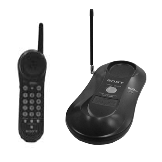
Photo : SPP-N1003
SPECIFICATIONS
General
Operating frequency
902-928 MHz (0.3mW)
Frequency control
Crystal-controlled PLL
Operation mode
FM, duplex
Operation channel
30 channels
Supplied accessories
AC power adaptor AC-T127
Telephone line cord
Headset TL-HD10, for the use of the left ear only (SPP-N1003)
Rechargeable battery pack BP-T50G
Directories (2 sheets)
Handset
Power source
Rechargeable battery pack BP-T50
Battery life
Standby: Approx. 30 days
Talk:
Dimensions
Approx. 2
(approx. 55 x 180 x 48 mm)
Antenna: Approx. 1
Antenna: Approx. 1
Mass
Approx. 5.5 oz (approx. 155 g), battery included
Base unit
Power source
DC 9V from AC power adaptor
Battery charging time Approx. 12 hours
Dimensions
Approx. 3
(approx. 97 x 52 x 212 mm) (SPP-N1001)
Approx. 4
(approx. 107 x 52 x 212 mm) (SPP-N1003)
Antenna: Approx. 4
Mass
Approx. 7.6 oz (approx. 215 g)
Head set (TL-HD10, for the use of the left ear only) (SPP-N1003)
Cord length
Approx. 47
Mass
Approx. 2 oz (approx. 55 g)
Design and specifications are subjec to change without notice.
Approx. 10 hours
1
/
x 7
1
/
x 1
15
/
inches (w/h/d), antenna excluded
4
8
16
1
/
inches (approx. 27 mm) (SPP-N1001)
8
15
/
inches (approx. 48 mm) (SPP-N1003)
16
7
1
3
/
x 2
/
x 8
/
inches (w/h/d)
8
8
8
1
1
3
/
x 2
/
x 8
/
inches (w/h/d), antenna excluded
4
8
8
5
/
inches (approx. 115 mm) (SPP-N1003)
8
1
/
inches (approx. 1.2 m)
4
CORDLESS TELEPHONE
US Model
SPP-N1003
Canadian Model
SPP-N1001/N1003
E Model
SPP-N1001
Advertisement
Table of Contents

Related Manuals for Sony SPP-N1001


Summary of Contents for Sony SPP-N1001
- Page 1 DC 9V from AC power adaptor Battery charging time Approx. 12 hours Dimensions Approx. 3 inches (w/h/d) (approx. 97 x 52 x 212 mm) (SPP-N1001) Approx. 4 inches (w/h/d), antenna excluded (approx. 107 x 52 x 212 mm) (SPP-N1003) Antenna: Approx. 4 inches (approx.
-
Page 2: Table Of Contents
LES COMPOSANTS IDENTIFIÉS PAR UNE MARQUE ! SUR LES DIAGRAMMES SCHÉMATIQUES ET LA LISTE DES PIÈCES SONT CRITIQUES POUR LA SÉCURITÉ DE FONCTIONNEMENT. NE REMPLACER CES COMPOSANTS QUE PAR DES PIÈCES SONY DONT LES NUMÉROS SONT DONNÉS DANS CE MANUEL OU DANS LES SUPPLÉMENTS PUBLIÉS PAR SONY. - Page 3 SECTION 1 This section is extracted from GENERAL instruction manual. – 3 –...
- Page 4 – 4 –...
- Page 5 (SPP-N1003) – 5 –...
-
Page 6: Disassembly
SECTION 2 DISASSEMBLY The equipment can be removed using the following procedure. Base unit Cabinet (upper) Base main board Handset Cabinet (rear) Jack board (SPP-N1003 only) Hand main board Note : Follow the disassembly procedure in the numerical order given. 2-1. -
Page 7: Cabinet (Rear)
2-3. CABINET (REAR) Cabinet (rear) 3 Claws Cabinet (front) Cabinet (rear) 2 Screws (+BTP 2.6x12) 3 Claws Cabinet (rear) Lid, battery case Cabinet (front) Cabinet (front) 2-4. JACK BOARD (SPP-N1003 ONLY) Cabinet (front) CN801 1 Screws (+BTP 2.6x8) Jack board Cabinet (rear) 2 Claws –... -
Page 8: Hand Main Board
2-5. HAND MAIN BOARD 2 Screws (+BTP 2.6x10) 1 Remove solder Cover (antenna) Hand main board Black Cabinet (front) – 8 –... -
Page 9: Test Mode
SECTION 3 TEST MODE BASE UNIT MANUAL TEST MODE HANDSET MANUAL TEST MODE 1 Base Unit Manual Test Mode Startup Procedure 1 Handset Manual Test Mode Startup Procedure 1. Turn on the power while holding down the HANDSET LO- CATOR key, then perform the following steps within 10 sec- 1. - Page 10 4 Power Saving Measurement Mode To enter power saving measurement mode, press one of the 7, 8, 9 keys while in test idle mode. Pressing the OFF key after enter- ing power saving measurement mode returns the operation to test idle mode.
-
Page 11: Electrical Adjustments
SECTION 4 ELECTRICAL ADJUSTMENTS BASE UNIT RX ADJUSTMENT BASE UNIT 1. Transmit Mode Setting Procedure BASE UNIT TX ADJUSTMENT 1. Start up the test mode according to the Manual Test Mode 1. Transmit Mode Setting Procedure Startup Procedure. (See page 9) 1. - Page 12 Connection and adjustment location : BASE MAIN BOARD (SIDE B) FM RF signal generator (VDD) TP406 (ANT) TP407 (RF GND) oscilloscope TP406 (ANT) digital TP407 voltmeter (RF GND) frequency counter TP401 (RSSI) TP406 (ANT) TP407 (RF GND) digital voltmeter TP404 (AF OUT) BASE MAIN BOARD (SIDE A) audio analyzer...
- Page 13 HANDSET RX CHECK HANDSET 1 Initial Settings HANDSET TX ADJUSTMENT 1. Start up test mode according to the “Manual Test Mode Startup 1 Initial Settings Procedure”. (See page 9) 1. Start up test mode according to the “Manual Test Mode Startup 2.
- Page 14 Connection and adjustment location : FM RF signal generator oscilloscope TP401 (ANT) TP402 (RF GND) HAND MAIN BOARD (SIDE B) frequency counter TP401 (ANT) TP409 (SPB) TP402 150 Ω TP408 (RF GND) (SPR) digital voltmeter audio analyzer TP403 (AF OUT) TP408 (SPR) TP409 (SPB) CT501: TX Frequency adjustmernt...
-
Page 15: Explanation Of Ic Terminals
SECTION 5 DIAGRAMS 5-1. EXPLANATION OF IC TERMINALS IC501 TMP87CH847U-1K06 (BASE UNIT SYSTEM CONTROL) Pin No. Pin name Description RF CLK Serial clock output. DTMF LA Latch output for DTMF IC. QUICK CHG Quick charge control output. RX DATA RX data input. —... - Page 16 IC501 TMP87CH47LU-1K07 (HAND SET SYSTEM CONTROL) Pin No. Pin name Description RF CLK Serial clock output. RING OUT Beep signal output. RING VOL Beep signal volume control RX DATA RX data input. VOL SW2 VOL switch input 1. VOL SW1 VOL switch input 2.
-
Page 17: Block Diagrams (Base Unit Section)
SPP-N1001/N1003 5-2. BLOCK DIAGRAMS (BASE UNIT SECTION) • Signal path. • Abbreviation : RX CND : Canadian : TX C&SA : Central and South America : bell – 17 – – 18 –... -
Page 18: Block Diagrams (Handset Section)
SPP-N1001/N1003 5-3. BLOCK DIAGRAMS (HANDSET SECTION) • Signal path. : RX : TX : bell • Abbreviation CND : Canadian C&SA : Central and South America – 19 – – 20 –... - Page 19 SPP-N1001/N1003 5-4. PRINTED WIRING BOARDS (BASE UNIT SECTION) Semiconductor Location J101 Ref. No. Location LINE DC IN 9V ANT1 D101 ANTENNA D201 BASE MAIN BOARD (SIDE B) BASE MAIN BOARD (SIDE A) D203 D204 D211 D301 D302 F-11 D401 E-10...
- Page 20 SPP-N1001/N1003 5-5. SCHEMATIC DIAGRAM (BASE UNIT SECTION) Note: Waveform • All capacitors are in µF unless otherwise noted. pF: µµF • Signal path. : RX 50 WV or less are not indicated except for electrolytics : TX and tantalums. • All resistors are in Ω and...
- Page 21 SPP-N1001/N1003 5-6. PRINTED WIRING BOARDS (HANDSET SECTION) Semiconductor Location ANT2 Ref. No. Location ANTENNA N1001:Canadian, C&SA/ D301 HAND MAIN BOARD (SIDE B) N1003:US, Canadian MODEL D302 D303 BZ601 D401 BUZZER D402 E-11 D501 SPP-N1001 D502 D503 SP401 SPEAKER D701 –...
- Page 22 SPP-N1001/N1003 5-7. SCHEMATIC DIAGRAM (HANDSET SECTION) Refer to page 26 for Waveform. Refer to page 26 for Notes. – 27 – – 28 –...
- Page 23 SPP-N1001/N1003 5-8. PRINTED WIRING BOARDS (JACK SECTION) (SPP-N1003 ONLY) 5-9. SCHEMATIC DIAGRAM (JACK SECTION) (SPP-N1003 ONLY) JACK BOARD J801 Q801 (11) 1-678-426- (FOMER TYPE) HAND MAIN BOARD (NEW TYPE) HAND MAIN BOARD HAND MAIN BOARD (NEW TYPE) (FORMER TYPE)(Page 26) Note: •...
- Page 24 SECTION 6 EXPLODED VIEWS NOTE : • -XX, -X mean standardized parts, so they • The mechanical parts with no reference The components identified by mark 0 may have some difference from the original number in the exploded views are not or dotted line with mark 0 are critical one.
- Page 25 6-2. HANDSET SECTION N1003 SP401 N1001 BZ601 MIC401 Ref. No. Part No. Description Remark Ref. No. Part No. Description Remark * 51 A-3622-470-A HAND MAIN BOARD, COMPLETE (N1003) 3-046-099-01 CABINET (REAR) (GRAY) (N1001) * 51 A-3673-082-A HAND MAIN BOARD, COMPLETE (N1001:CND) 3-046-099-11 CABINET (REAR) (WHITE) (N1001:CND) * 51 A-3673-110-A HAND MAIN BOARD, COMPLETE...
- Page 26 6-3. HEAD SET SECTION (SPP-N1003 ONLY) not supplied not supplied not supplied not supplied D901 not supplied MIC501 not supplied not supplied Ref. No. Part No. Description Remark Ref. No. Part No. Description Remark X-3379-350-1 HEAD SET ASSY (N1003) 1-757-133-11 CORD (WITH PLUG) (N1003) 3-220-095-01 EAR PAD (N1003) D901 8-719-069-55 DIODE UDZS-TE17-5.6B (N1003)
- Page 27 SECTION 7 BASE MAIN ELECTRICAL PARTS LIST NOTE : • Due to standardization, replacements in the • SEMICONDUCTORS In each case, u : µ , for example : The components identified by mark 0 parts list may be different from the parts or dotted line with mark 0 are critical uA..
- Page 28 BASE MAIN Ref. No. Part No. Description Remark Ref. No. Part No. Description Remark C461 1-107-826-11 CERAMIC CHIP 0.1uF < IC > C462 1-162-968-11 CERAMIC CHIP 0.0047uF 10% C463 1-162-967-11 CERAMIC CHIP 0.0033uF 10% IC401 8-759-672-68 IC IC TB31261AF(EL) C464 1-126-163-11 ELECT 4.7uF IC501...
- Page 29 BASE MAIN Ref. No. Part No. Description Remark Ref. No. Part No. Description Remark R202 1-215-878-00 METAL OXIDE R429 1-414-229-11 INDUCTOR R203 1-216-037-00 METAL CHIP 1/10W R430 1-216-816-11 METAL CHIP 1/16W R431 1-216-811-11 METAL CHIP 1/16W R204 1-216-845-11 METAL CHIP 100K 1/16W R432...
- Page 30 BASE MAIN HAND MAIN Ref. No. Part No. Description Remark Ref. No. Part No. Description Remark < VARIABLE RESISTOR > C426 1-162-921-11 CERAMIC CHIP 33PF C427 1-162-910-11 CERAMIC CHIP 0.25PF 50V RV401 1-225-907-21 RES, ADJ, CERMET (3 TYPE) 100K C428 1-162-912-11 CERAMIC CHIP 0.5PF (RSSI(H)SENS)
- Page 31 HAND MAIN Ref. No. Part No. Description Remark Ref. No. Part No. Description Remark C475 1-162-968-11 CERAMIC CHIP 0.0047uF 10% L402 1-469-633-21 INDUCTOR 18nH C476 1-107-826-11 CERAMIC CHIP 0.1uF L404 1-414-735-21 INDUCTOR 5.6nH C477 1-165-176-11 CERAMIC CHIP 0.047uF L405 1-469-632-21 INDUCTOR 15nH (A TYPE) C478 1-162-918-11 CERAMIC CHIP...
- Page 32 HAND MAIN Ref. No. Part No. Description Remark Ref. No. Part No. Description Remark R416 1-216-818-11 METAL CHIP 1/16W R508 1-216-861-11 METAL CHIP 2.2M 1/16W R418 1-216-833-11 METAL CHIP 1/16W R509 1-216-849-11 METAL CHIP 220K 1/16W (A TYPE) R512 1-216-821-11 METAL CHIP 1/16W R418 1-216-835-11 METAL CHIP...
- Page 33 SPP-N1001/N1003 JACK Ref. No. Part No. Description Remark Ref. No. Part No. Description Remark A-3622-433-A JACK BOARD, COMPLETE (N1003) MISCELLANEOUS ********************* ************** < CAPACITOR > 1-771-940-11 SWITCH, RUBBER KEY * 60 A-3622-433-A JACK BOARD, COMPLETE (N1003) C801 1-115-156-11 CERAMIC CHIP...
- Page 34 SPP-N1001/N1003 US Model SPP-N1003 Canadian Model SERVICE MANUAL SPP-N1001/N1003 E Model 2001. 05 SPP-N1001 SUPPLEMENT - 1 File this Supplement with the Service Manual. Subject : ARGENTINA MODEL HAS BEEN ADDED FOR SPP-N1001 ECHANGE OF BOARDS BASE MAIN BOARD:1-678-635-12 , 1-681-415-11...
- Page 35 SPP-N1001/N1003 • CHANGE OF BOARDS Base main board and hand main board has been changed. Printed wiring board and schematic diagram of new type, and changed parts list are described in this Supplement-1. Refer to original service nanual (9-927-979-11) previously issued for other information.
-
Page 36: Printed Wiring Boards (Base Unit Section)
SPP-N1001/N1003 PRINTED WIRING BOARDS (BASE UNIT SECTION) Semiconductor Location J101 Ref. No. Location LINE DC IN 9V D101 BASE MAIN BOARD (SIDE B) BASE MAIN BOARD (SIDE A) D201 D203 D204 D211 D401 D402 E-10 D403 D501 D502 IC401 F-10... -
Page 37: Schematic Diagram (Base Unit Section)
SPP-N1001/N1003 SCHEMATIC DIAGRAM (BASE UNIT SECTION) Note: Waveform • All capacitors are in µF unless otherwise noted. pF: µµF • Signal path. : RX 50 WV or less are not indicated except for electrolytics and tantalums. : TX • All resistors are in Ω and... -
Page 38: Printed Wiring Boards (Handset Section)
SPP-N1001/N1003 PRINTED WIRING BOARDS (HANDSET SECTION) Semiconductor Location Ref. No. Location ANT2 D302 ANTENNA EXCEPT D303 HAND MAIN BOARD (SIDE B) MX MODEL D304 D401 N1001 BZ601 D402 E-11 BUZZER N1001 D501 D502 SPP-N1001 D504 D701 SP401 D702 – SPEAKER... -
Page 39: Schematic Diagram (Jack Section) (Spp-N1003 Only)
SPP-N1001/N1003 SCHEMATIC DIAGRAM (HANDSET SECTION) Refer to page 5 for Waveform. Refer to page 5 for Notes. -
Page 40: Exploded Views
SPP-N1001/N1003 EXPLODED VIEWS NOTE : • -XX, -X mean standardized parts, so they • The mechanical parts with no reference The components identified by mark 0 may have some difference from the original number in the exploded views are not or dotted line with mark 0 are critical one. -
Page 41: Handset Section
SPP-N1001/N1003 6-2. HANDSET SECTION N1003 SP401 N1001 BZ601 MIC401 Ref. No. Part No. Description Remark Ref. No. Part No. Description Remark * 51 A-3021-463-A HAND MAIN BOARD, COMPLETE (N1003) 3-046-099-01 CABINET (REAR) (GRAY) (N1001) * 51 A-3021-456-A HAND MAIN BOARD, COMPLETE (N1001:CND) -
Page 42: Electrical Parts List
SPP-N1001/N1003 BASE MAIN ELECTRICAL PARTS LIST NOTE : • Due to standardization, replacements in the • SEMICONDUCTORS In each case, u : µ , for example : The components identified by mark 0 parts list may be different from the parts or dotted line with mark 0 are critical uA.. - Page 43 SPP-N1001/N1003 BASE MAIN Ref. No. Part No. Description Remark Ref. No. Part No. Description Remark C507 1-162-970-11 CERAMIC CHIP 0.01uF <TRANSISTOR> C508 1-162-964-11 CERAMIC CHIP 0.001uF C509 1-162-970-11 CERAMIC CHIP 0.01uF Q101 8-729-920-85 TRANSISTOR 2SD1664-QR C510 1-164-245-11 CERAMIC CHIP 0.015uF...
- Page 44 SPP-N1001/N1003 BASE MAIN HAND MAIN Ref. No. Part No. Description Remark Ref. No. Part No. Description Remark R417 1-216-847-11 METAL CHIP 150K 1/16W R536 1-216-846-11 METAL CHIP 120K 1/16W R418 1-216-864-11 METAL CHIP 1/16W R537 1-216-846-11 METAL CHIP 120K 1/16W...
- Page 45 SPP-N1001/N1003 HAND MAIN Ref. No. Part No. Description Remark Ref. No. Part No. Description Remark C420 1-107-826-11 CERAMIC CHIP 0.1uF C478 1-162-918-11 CERAMIC CHIP 18PF C421 1-164-230-11 CERAMIC CHIP 220PF C479 1-162-927-11 CERAMIC CHIP 100PF C422 1-162-964-11 CERAMIC CHIP 0.001uF...
- Page 46 SPP-N1001/N1003 HAND MAIN Ref. No. Part No. Description Remark Ref. No. Part No. Description Remark L410 1-414-721-11 INDUCTOR 10nH L411 1-412-987-31 INDUCTOR 4.7uH R429 1-216-829-11 METAL CHIP 4.7K 1/16W R431 1-216-825-11 METAL CHIP 2.2K 1/16W <MICROPHONE> R432 1-216-821-11 METAL CHIP...
- Page 47 SPP-N1001/N1003 HAND MAIN Ref. No. Part No. Description Remark Ref. No. Part No. Description Remark R522 1-216-845-11 METAL CHIP 100K 1/16W ACCESSORIES & PACKING MATERIALS R523 1-216-857-11 METAL CHIP 1/16W ******************************* R524 1-216-845-11 METAL CHIP 100K 1/16W 1-476-067-11 ADAPTOR, AC (AC-T125) (N1001:AR)
- Page 48 SPP-N1001/N1003...
- Page 49 Clicking the version allows you to jump to the revised page. Also, clicking the version at the upper right on the revised page allows you to jump to the next revised page. Ver. Date Description of Revision 2001.05 SUPPLEMENT-1 : Argentina model added for SPP-N1001. Change of boards. (ENG-01005) 2000.08...