Table of Contents
Advertisement
Quick Links
SERVICE MANUAL
Ver 1.1 2001.12
General
Operating frequency
Base unit: 902 - 905 MHz (310µW)
Hand set: 925 - 928 MHz (400µW)
Operating channel
30 channels
Dial signal
Tone, 10 PPS (pulse) selectable
Supplied accessories
AC power adaptor AC-T122
Telephone line cord
Rechargeable battery pack BP-T18
Belt clip
Wall bracket
Handset
Power source
Rechargeable battery pack BP-T18
Battery life
Standby: Approx. 7 days
Talk:
Dimensions
Approx. 2
antenna excluded
(approx. 55 x 47 x 183 mm)
Antenna: Approx. 1
(approx. 34 mm)
Mass
Approx. 7.7 oz (approx. 220 g), battery
included
Sony Corporation
9-873-145-12
2001L0500-1
Personal Audio Company
C 2001.12
Published by Sony Engineering Corporation
SPP-A1070/A1071
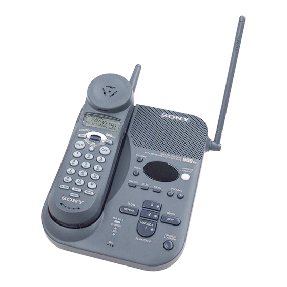
Photo: SPP-A1070
SPECIFICATIONS
Approx. 7 hours
1
7
1
⁄
x 1
⁄
x 7
⁄
inches (w/h/d),
4
8
4
3
⁄
inches
8
CORDLESS TELEPHONE WITH ANSWERING SYSTEM
Base unit
Power source
DC 9V from AC power adaptor AC-T122
Battery charging time
Approx. 12 hours
Dimensions
3
1
1
Approx. 6
⁄
x 2
⁄
x 7
⁄
inches (w/h/d),
4
4
2
antenna excluded
(approx. 171 x 57 x 189 mm)
1
Antenna: Approx. 6
⁄
inches
8
(approx. 153 mm)
Mass
Approx. 15 oz (approx. 412 g), wall bracket
excluded
Answering machine
Maximum recording time
Approx. 15 minutes, using incorporated IC
Greeting message
Up to 90 seconds per each
Incoming Memo message
Up to 4 minutes per message
Design and specifications are subject to
change without notice.
US Model
SPP-A1070
Canadian Model
SPP-A1071
Advertisement
Table of Contents

Related Manuals for Sony SPP-A1071


Summary of Contents for Sony SPP-A1071
- Page 1 Design and specifications are subject to change without notice. Antenna: Approx. 1 ⁄ inches (approx. 34 mm) Mass Approx. 7.7 oz (approx. 220 g), battery included CORDLESS TELEPHONE WITH ANSWERING SYSTEM Sony Corporation 9-873-145-12 2001L0500-1 Personal Audio Company C 2001.12 Published by Sony Engineering Corporation...
-
Page 2: Table Of Contents
SUR LES DIAGRAMMES SCHÉMATIQUES ET LA LISTE DES PIÈCES SONT CRITIQUES POUR LA SÉCURITÉ DE FONCTIONNEMENT. NE REMPLACER CES COM- POSANTS QUE PAR DES PIÈCES SONY DONT LES NUMÉROS SONT DONNÉS DANS CE MANUEL OU DANS LES SUPPLÉMENTS PUBLIÉS PAR SONY. - Page 3 SPP-A1070 : Serial No. 0316344 or later that board, but replace with an former type board (BASE MAIN SPP-A1071 : Serial No. A0103501 or later board : Part No. A-3062-656-A, HAND MAIN board : Part No. A-3062-658-A (A1070)/A-3062-742-A(A1071)). In this case, re- move the EEPROM (BASE MAIN board : Ref No.
-
Page 4: General
SPP-A1070/A1071 SECTION 2 This section is extracted from instruction manual. GENERAL Identifying the parts Refer to the pages indicated in parentheses for details. Base Unit w; wa 1 Message counter (p. 35, 61) 6 REPEAT/SLOW button (p. 37) qd Speaker (p. 38) ql Hook for AC power adaptor cord (p. -
Page 5: Disassembly
SPP-A1070/A1071 SECTION 3 DISASSEMBLY • This set can be disassembled in the order shown below. 3-1. DISASSEMBLY FLOW HAND MAIN board H/S rear assy H/S FRT assy Base bottom BASE MAIN board Note: Follow the disassembly procedure in the numerical order given. 3-2. -
Page 6: H/S Frt Assy
SPP-A1070/A1071 3-3. H/S FRT ASSY 1 screw (BTP2.6 × 8) 3 screw (BTP2.6 × 8) 4 two screws (P2 × 5) 6 H/S FRT assy 3-4. HAND MAIN BOARD 5 screw (BTP2.6 × 8) 6 RF unit (hand) 8 receiver BKT 4 Remove twelve solders. -
Page 7: Base Bottom
SPP-A1070/A1071 3-5. BASE BOTTOM 2 claw 1 five screws (P3 × 12) 3 base bottom 2 claw 3-6. BASE MAIN BOARD 6 two screws (BTP2.6 × 8) 8 BASE MAIN board 3 screw (BTP2.6 × 8) 7 two screws (BTP2.6 × 6) 4 RF unit (base) 2 harness 1 Remove solder of lead. -
Page 8: Test Mode
SPP-A1070/A1071 SECTION 4 TEST MODE Introduction 4. Data Link Data bits are encoded in manchester format for which bit “0” is The manual test mode can be used for testing the RF and audio represented by 500 µs low and 500 µs high while bit “1” by 500 sections of the base unit and handset. - Page 9 SPP-A1070/A1071 3. Key Definition 4. Data Link Data bits are encoded in manchester format for which bit “0” is represented by 500 µs high and 500 µs low while bit “1” by 500 Operation: Set combo to inactive mode. µs low and 500 µs high. Indication: CB=0 If data transmission is enabled, it will transmit data packet with the following fields continuously.
- Page 10 SPP-A1070/A1071 Frequency Allocation Tables Base Unit Frequencies: Handset Frequencies: Transmit Receive RX LO Transmit Receive RX LO Channel Channel Frequency Frequency Frequency Frequency Frequency Frequency 902.30 MHz 925.05 MHz 935.75 MHz 925.05 MHz 902.30 MHz 891.60 MHz 903.35 MHz 926.10 MHz 936.80 MHz 926.10 MHz 903.35 MHz...
-
Page 11: Diagrams
SPP-A1070/A1071 SECTION 5 DIAGRAMS 5-1. BLOCK DIAGRAM – BASE UNIT Section – D1 – D4 RECT RF UNIT LINE TRANSFORMER AF AMP BUFFER LINE LINE TX (FOR TX) U2 (1/4) FREQUENCY SHIFT KEYING DEMODULATOR HOOK ON/OFF RX DATA RX DATA AF AMP RLL DATA PLL DATA... -
Page 12: Block Diagram - Handset Section
SPP-A1070/A1071 5-2. BLOCK DIAGRAM – HANDSET Section – RF UNIT • SIGNAL PATH : TX 29 TX DATA TX DATA : RX 14 PLL EN PLL EN LCD1 PLL CLK 15 PLL CLK LIQUID CRYSTAL PLL I2C DATA 16 PLL I2C DATA DISPLAY MODULE EEPROM 17 I2C CLK... -
Page 13: Note For Printed Wiring Boards And Schematic Diagrams
SPP-A1070/A1071 5-3. NOTE FOR PRINTED WIRING BOARDS AND SCHEMATIC DIAGRAMS • IC Block Diagrams – BASE MAIN Board – Note on Printed Wiring Board: Note on Schematic Diagram: • All capacitors are in µF unless otherwise noted. pF: µµF • X : parts extracted from the component side. U3 PCC318 •... -
Page 14: Printed Wiring Board - Base Main Board
SPP-A1070/A1071 5-4. PRINTED WIRING BOARD – BASE MAIN Board – BASE MAIN BOARD E C B E C B E C B CHARGE CHARGE TERMINAL TERMINAL LINE LINE TRANSFORMER – DC IN 9V MIC101 EC14 BASE KEY UNIT BOARD (Page 16) R106 R103 R100... -
Page 15: Schematic Diagram - Base Main Board
SPP-A1070/A1071 5-5. SCHEMATIC DIAGRAM – BASE MAIN Board – • • See page 13 for Waveforms. See page 13 for IC Block Diagrams. 1N4148 MMBT3906 MC78M05CT +5V REGULATOR TP10 Q7,8 10µH 10µH CHARGE CONTROL BAV99L HZ27-1L HZ27-1L TP18 TP11 10µH 10µH 6.3V MMBT3906... -
Page 16: Printed Wiring Board - Base Key Board
SPP-A1070/A1071 5-6. PRINTED WIRING BOARD – BASE KEY Board – 5-7. SCHEMATIC DIAGRAM – BASE KEY Board – (Page 15) • Semiconductor Location Ref. No. Location LED1 LED2 LED3 LED4 LED5 LED6 LED7 (Page 14) -
Page 17: Ic Pin Function Description
SPP-A1070/A1071 5-8. IC PIN FUNCTION DESCRIPTION • BASE MAIN BOARD U4 TMP86CM25F-3CR3 (SYSTEM CONTROLLER) • HAND MAIN BOARD U2 TMP87C807U-3CR4 (SYSTEM CONTROLLER) Pin No. Pin Name Description Pin No. Pin Name Description — Ground terminal CIDSCL Caller-ID clock signal output to the PCC318 (U3) Main system clock input terminal (8 MHz) CIDSDA Caller-ID two-way data bus with the PCC318 (U3) -
Page 18: Printed Wiring Board - Hand Main Board
SPP-A1070/A1071 5-9. PRINTED WIRING BOARD – HAND MAIN Board – • Semiconductor Location Ref. No. Location CHARGE TERMINAL –... -
Page 19: Schematic Diagram - Hand Main Board
SPP-A1070/A1071 5-10. SCHEMATIC DIAGRAM – HAND MAIN Board – • See page 13 for Waveforms. 24WC32 COM0 COM1 100k COM2 COM3 COM4 UNIT COM5 COM2 SEG28 COM6 COM2 SEG28 100k COM3 SEG29 EEPROM SEG5 COM3 SEG29 COM4 SEG30 SEG6 COM4 SEG30 COM5 SEG31... -
Page 20: Exploded Views
SPP-A1070/A1071 Ver 1.1 SECTION 6 EXPLODED VIEWS NOTE: 6-2. BASE SET SECTION • -XX and -X mean standardized parts, so they • Items marked “*” are not stocked since they may have some difference from the original are seldom required for routine service. Some one. -
Page 21: Electrical Parts List
SPP-A1070/A1071 SECTION 7 ELECTRICAL PARTS LIST BASE KEY BASE MAIN NOTE: • Due to standardization, replacements in the • Items marked “*” are not stocked since they The components identified by mark 0 or dotted line with mark parts list may be different from the parts speci- are seldom required for routine service. - Page 22 SPP-A1070/A1071 BASE MAIN Ref. No. Part No. Description Remark Ref. No. Part No. Description Remark EC11 1-126-933-11 ELECT 100uF EC12 1-126-964-11 ELECT 10uF 1-218-306-11 METAL CHIP 100K 1/16W EC13 1-126-964-11 ELECT 10uF 1-216-843-11 METAL CHIP 1/16W EC14 1-126-935-11 ELECT 470uF 6.3V 1-249-608-11 CARBON 220K...
- Page 23 SPP-A1070/A1071 BASE MAIN HAND MAIN Ref. No. Part No. Description Remark Ref. No. Part No. Description Remark 1-216-826-11 METAL CHIP 2.7K 1/16W 1-164-874-11 CERAMIC CHIP 100PF 1-216-833-11 METAL CHIP 1/16W 1-107-826-11 CERAMIC CHIP 0.1uF 1-216-834-11 METAL CHIP 1/16W 1-107-826-11 CERAMIC CHIP 0.1uF 1-127-715-11 CERAMIC CHIP 0.22uF...
- Page 24 SPP-A1070/A1071 HAND MAIN Ref. No. Part No. Description Remark Ref. No. Part No. Description Remark < RESISTOR > < VIBRATOR > 1-216-845-11 METAL CHIP 100K 1/16W 1-216-845-11 METAL CHIP 100K 1/16W 1-760-627-11 VIBRATOR, CRYSTAL (32.768kHz) 1-216-821-11 METAL CHIP 1/16W 1-567-918-21 VIBRATOR, CERAMIC (8MHz) 1-216-799-11 METAL CHIP 1/16W ************************************************************...
- Page 25 SPP-A1070/A1071 MEMO...
-
Page 26: Revision History
Also, clicking the version at the upper right on the revised page allows you to jump to the next revised page. Ver. Date Description of Revision 2001.12 Change of BASE MAIN/HAND MAIN boards (ENG-01025) Addition of BASE TOP and BASE BOTTOM for SPP-A1071 (SPM-01054) 2001.06...