Sony Cybershot DSC-T9 Service Manual
Digital still camera
Hide thumbs
Also See for Cybershot DSC-T9:
- Guia del usuario/solucion de problemas (227 pages) ,
- User's manual / troubleshooting (111 pages) ,
- Operating instructions (2 pages)
Table of Contents
Advertisement
Quick Links
Download this manual
See also:
Operating Instructions
SERVICE MANUAL
Ver 1.1 2005.12
Revision History
Revision History
How to use
How to use
Acrobat Reader
Acrobat Reader
Internal memory
Internal memory
ON BOARD
ON BOARD
Link
Link
SPECIFICATIONS
SERVICE NOTE
DISASSEMBLY
• Precaution on Replacing the SY-141 Board
The components identified by
mark 0 or dotted line with
mark 0 are critical for safety.
Replace only with part num-
ber specified.
DSC-T9_L2
9-876-911-31
BLOCK DIAGRAMS
FRAME SCHEMATIC DIAGRAM
SCHEMATIC DIAGRAMS
Les composants identifiés par une
marque 0 sont critiques pour la
sécurité.
Ne les remplacer que par une pièce
portant le numéro spécifié.
Sony EMCS Co.
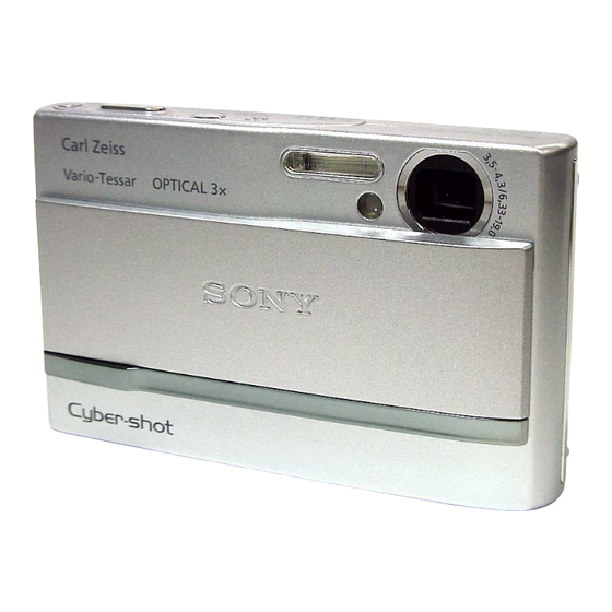
DSC-T9
Photo: Silver
DIGITAL STILL CAMERA
LEVEL
US Model
Canadian Model
AEP Model
UK Model
E Model
Australian Model
Hong Kong Model
Chinese Model
Korea Model
Brazilian Model
Japanese Model
Tourist Model
PRINTED WIRING BOARDS
REPAIR PARTS LIST
Published by DI Technical Support Department
2
2005L0500-1
© 2005.12
Advertisement
Table of Contents

Related Manuals for Sony Cybershot DSC-T9


Summary of Contents for Sony Cybershot DSC-T9
- Page 1 0 are critical for safety. sécurité. Replace only with part num- Ne les remplacer que par une pièce ber specified. portant le numéro spécifié. DIGITAL STILL CAMERA 2005L0500-1 DSC-T9_L2 © 2005.12 Sony EMCS Co. 9-876-911-31 Published by DI Technical Support Department...
- Page 2 SPECIFICATIONS Camera [Power, general] BC-CS3 battery charger Power Rechargeable battery pack NP- [System] Power requirements FT1, 3.6 V AC 100 to 240 V, 50/60 Hz, Image device 7.181 mm (1/2.5 type) color 3.2 W AC-LS5K AC Adaptor (not CCD, Primary color filter supplied), 4.2 V Output voltage DC 4.2 V, 500 mA...
- Page 3 CRITIQUES POUR LA SÉCURITÉ DE FONCTIONNEMENT. NE COMPONENTS WITH SONY PARTS WHOSE PART NUMBERS REMPLACER CES COMPOSANTS QUE PAR DES PIÈSES SONY APPEAR AS SHOWN IN THIS MANUAL OR IN SUPPLEMENTS DONT LES NUMÉROS SONT DONNÉS DANS CE MANUEL OU PUBLISHED BY SONY.
-
Page 4: Table Of Contents
TABLE OF CONTENTS Section Title Page Section Title Page SERVICE NOTE 1-1. Description on Self-diagnosis Display ···························· 1-1 1-2. Process After Fixing Flash Error ····································· 1-1 1-3. Method for Copying or Erasing the Data in Internal Memory ··········································································· 1-2 1-4. Precaution on Replacing the SY-141 Board ···················· 1-3 DISASSEMBLY 2-1. -
Page 5: Service Note
1-1. DESCRIPTION ON SELF-DIAGNOSIS DISPLAY Self-diagnosis display • C: ss: ss You can reverse the camera malfunction yourself. (However, contact your Sony dealer or local authorized Sony service facility when you cannot recover from the camera malfunction.) • E: ss: ss Contact your Sony dealer or local authorized Sony service facility. - Page 6 1-3. METHOD FOR COPYING OR ERASING THE DATA IN INTERNAL MEMORY (INTERNAL MEMORY/MUSIC) The data can be copied/erased by the operations on the Setup screen. (When erasing the data, execute formatting the internal memory.) Note 1: When replacing the SY-141 board, erase the data in internal memory of the board before replacement. Note 2: When replacing the SY-141 board or the IC401 on the SY-141 board, execute formatting and initialize the internal memory after replacement.
-
Page 7: Precaution On Replacing The Sy-141 Board
1-4. PRECAUTION ON REPLACING THE SY-141 BOARD VIDEO OUT Default Data Check When you replace to the repairing board, the written data of repairing board also might be changed to original setteing because of broadcast system (NTSC/PAL). When the data has changed because of board replaceing etc, check the default data of VIDEO OUT if destination code is right. If not, rewrite to the right value. - Page 8 2. DISSASSEMBLY NOTE FOR REPAIR • Make sure that the flat cable and flexible board are not cracked of bent at the terminal. Cut and remove the part of gilt Do not insert the cable insufficiently nor crookedly. which comes off at the point. (Be careful or some •...
-
Page 9: Disassembly
HELP HELP The following flow chart shows the disassembly procedure. 2-1. DISASSEMBLY 1 P2 Screw (M1.4x2.5) (silver)/(black) x5 1 P2 Screw (M1.4x2.5) (silver)/(black) x1 1 Connector x1 2 Claw x2 2 Tripod screw x1 2 Hook x2 3 Cabinet (front) assembly 3 Claw x1 3 Claw x2 4 Flexible board x2... - Page 10 HELP Sheet attachment positions and procedures of processing the flexible boards/harnesses are shown. SY board ST insulating sheet ST-131 board SY insulating sheet Control switch block (SW51800) hole hole Frame assembly SP insulating sheet SP frame DSC-T9_L2 HELP...
- Page 11 Frame assembly 0~1mm CD radiation sheet MC radiation sheet MC radiation sheet 0~0.5mm Fold MC-159 flexible board DSC-T9_L2 HELP...
- Page 12 MC conductive sheet MC conductive sheet (It pasted in the area.) Note for installation of Control switch block (RL51800) and Cabinet (rear) block. Control switch block (RL51800) Position of mode knob Mode knob Cabinet (rear) block Position of mode slider Mode slider Connector Claw...
-
Page 13: Block Diagrams
3. BLOCK DIAGRAMS Link Link OVERALL BLOCK DIAGRAM (1/2) POWER BLOCK DIAGRAM OVERALL BLOCK DIAGRAM (2/2) DSC-T9_L2... - Page 14 3. BLOCK DIAGRAMS 3-1. OVERALL BLOCK DIAGRAM (1/2) ( ) : Number in parenthesis ( ) indicates the division number of schematic diagram where the component is located. CD-597 FLEXIBLE BOARD SY-141 BOARD (1/2) LENS BLOCK IRIS LENS CN709 (METER) CN102 IC002 CCD_OUT...
-
Page 15: Overall Block Diagram (1/2)
3-2. OVERALL BLOCK DIAGRAM (2/2) ( ) : Number in parenthesis ( ) indicates the division number of schematic diagram where the component is located. SY-141 BOARD (2/2) CN704 MS_BS, MS_D0 – MS_D3, MS_CLK MS_BS, MS_D0 – MS_D3, MS_CLK MEMORY STICK V_LINE_OUT XMS_IN... -
Page 16: Power Block Diagram
3-3. POWER BLOCK DIAGRAM ( ) : Number in parenthesis ( ) indicates the division number of schematic diagram where the component is located. MC-159 SY-141 BOARD FLEXIBLE ST-131 BOARD T001 CN711 CN703 BOARD D001 F001 L001 ACV_UNREG ACV_UNREG ST_UNREG ST_UNREG FLASH UNIT... -
Page 17: Printed Wiring Boards And Schematic Diagrams
4. PRINTED WIRING BOARDS AND SCHEMATIC DIAGRAMS 4-1. FRAME SCHEMATIC DIAGRAM CN201 CONTROL CN001 IRIS_B CONTROL KEY_AD0 IRIS_A ST-131 SWITCH MIC901 IRIS_A D_3.2V SWITCH N.C. BOARD IRIS_B BLOCK KEY_AD1 N.C. BLOCK N.C. N.C. (FLASH DRIVE) FLASH UNIT (RL51800) REG_GND FC_SENS_GND (SW51800) FC_SENS_VCC FC_SENS... -
Page 18: Schematic Diagrams
4-2. SCHEMATIC DIAGRAMS Link Link BT-029 FLEXIBLE BOARD CD-597 FLEXIBLE BOARD (CCD IMAGER) (BATTERY IN, MODE SWITCH) CONTROL SWITCH BLOCK ST-131 BOARD (FLASH DRIVE) (RL51800, SW51800) MC-159 FLEXIBLE BOARD (MULTI CONNECTOR) COMMON NOTE FOR SCHEMATIC DIAGRAMS WAVEFORMS DSC-T9_L2... - Page 19 4-2. SCHEMATIC DIAGRAMS 4-2. SCHEMATIC DIAGRAMS 4-2. SCHEMATIC DIAGRAMS THIS NOTE IS COMMON FOR SCHEMATIC DIAGRAMS (In addition to this, the necessary note is printed in each block) (For schematic diagrams) 1. Connection • All capacitors are in µF unless otherwise noted. pF : µ Pattern box µF.
- Page 20 CD-597 FLEXIBLE BOARD Note: CD-597 flexible complete board, IC001 and IC002 are not supplied, but they are included in CCD block assy. CCD IMAGER Note: Voltages and Waveforms of IC001 can not be measured, because this is mounted by the side of the lens. XX MARK:NO MOUNT NO MARK:REC/PB MODE R:REC MODE...
- Page 21 Schematic diagrams of the SY-141 board are not shown. Pages from 4-9 to 4-20 are not shown. DSC-T9_L2...
- Page 22 • Refer to page 4-5 for mark 0. ST-131 BOARD FLASH DRIVE T001 D001 FT02P80TP XX MARK:NO MOUNT NO MARK:REC/PB MODE LND020 XE_H R003 1/10W ±5% LND018 TRIGGER FLASH UNIT LND019 TRIGGER_GND C328 C006 0.047u 315V LND001 STRB_CHARGE LND021 CHARGING LND002 PGND XSTRB_FULL...
- Page 23 • Refer to page 4-5 for mark 0. MC-159 FLEXIBLE BOARD BT-029 FLEXIBLE BOARD MULTI CONNECTOR BATTERY IN, MODE SWITCH XX MARK:NO MOUNT XX MARK:NO MOUNT R004 R005 2200 R003 PLAY 2200 ±5% 2200 ±5% ±5% LND001 ACV_GND LND001 MODE_DIAL0 S005 STILL LND002...
- Page 24 CONTROL SWITCH BLOCK (RL51800) CONTROL SWITCH BLOCK (RL51800) is replaced as block, so that PRINTED WIRING BOARD is omitted. D001 SML-412MWT86 (POWER) LND001 D_3.2V LND002 XPWR_LED S001 LND003 XPWR_ON POWER LND004 REG_GND CL001 LND005 MIC_SIG CL002 MIC901 S004 LND006 MIC_GND (SHUTTER) LND007 REG_GND...
-
Page 25: Printed Wiring Boards
4-3. PRINTED WIRING BOARDS Link Link CD-597 FLEXIBLE BOARD MC-159 FLEXIBLE BOARD ST-131 BOARD BT-029 FLEXIBLE BOARD COMMON NOTE FOR PRINTED WIRING BOARDS WAVEFORMS DSC-T9_L2... - Page 26 4-3. PRINTED WIRING BOARDS 4-3. PRINTED WIRING BOARDS 4-3. PRINTED WIRING BOARDS THIS NOTE IS COMMON FOR PRINTED WIRING BOARDS • : Uses unleaded solder. • Chip parts. • : Circuit board Transistor Diode : Flexible board Pattern from the side which enables seeing. : pattern of the rear side (The other layers’...
- Page 27 CD-597 (2 layers) : Uses unleaded solder. CD-597 FLEXIBLE BOARD 18 17 R004 R006 IC001 IC002 I < > P 1-868-927- 11 Note: CD-597 flexible complete board, IC001 and IC002 are not supplied, but they are included in CCD block assy. DSC-T9_L2 CD-597 4-29...
- Page 28 Printed wiring boards of the SY-141 board are not shown. Pages from 4-31 to 4-34 are not shown. DSC-T9_L2...
- Page 29 ST-131 (4 layers), MC-159 (2 layers), BT-029 (1 layer) : Uses unleaded solder. ST-131 BOARD FLASH UNIT XE_L XE_H TRIGGER_GND TRIGGER R002 R001 CAUTION C326 Danger of explosion if battery is incorrectly replaced. C001 Replace only with the same or equivalent type. D001 C328 S005...
-
Page 30: Waveforms
4-3. PRINTED WIRING BOARDS 4-3. PRINTED WIRING BOARDS 4-4. WAVEFORMS CD-597 FLEXIBLE BOARD 850 mVp-p IC002 3 REC DSC-T9_L2 CD-597 4-37... - Page 31 Waveforms of the SY-141 board are not shown. Pages 4-38 and 4-39 are not shown. DSC-T9_L2 4-38...
- Page 32 Mounted parts location of the SY-141 board is not shown. Page 4-40 is not shown. DSC-T9_L2 4-39...
-
Page 33: Repair Parts List
NOTE NOTE 5. REPAIR PARTS LIST NOTE: Characters A to Z of the electrical parts list indicate location of exploded views in which the desired part is shown. EXPLODED VIEWS EXPLODED VIEWS Link Link OVERALL SECTION SY BOARD SECTION FRAME SECTION ELECTRICAL PARTS LIST Link ELECTRICAL PARTS LIST... - Page 34 5. REPAIR PARTS LIST 5. REPAIR PARTS LIST 5. REPAIR PARTS LIST NOTE: • -XX, -X mean standardized parts, so they may have some differences from When indicating parts by reference number, the original one. please include the board name. •...
-
Page 35: Exploded Views
5. REPAIR PARTS LIST 5. REPAIR PARTS LIST 5-1. EXPLODED VIEWS 5-1-1. OVERALL SECTION ns: not supplied SY board section (See page 5-3.) (including CD-597 flexible board and IC001 (CCD imager)) (Note 1, 2) Note 1: CCD block assembly is including CD-597 flex- ible completed board and IC001 (CCD imager). - Page 36 5. REPAIR PARTS LIST 5. REPAIR PARTS LIST 5-1-2. SY BOARD SECTION ns: not supplied D901 LCD901 C328 Frame section (See page 5-4.) * Refer to the table of page 5-1 about language of SY-141 board. Refer to page 5-1 for mark 0. •...
- Page 37 5. REPAIR PARTS LIST 5. REPAIR PARTS LIST 5-1-3. FRAME SECTION ns: not supplied BH001 BT001 SP901 BT001 (BATTERY, LITHIUM SECONDARY) Board on the mount position (See page 4-36). CAUTION Danger of explosion if battery is incorrectly replaced. Replace only with the same or equivalent type. Refer to page 5-1 for mark 0.
-
Page 38: Electrical Parts List
BT-029 CD-597 MC-159 ST-131 5-2. ELECTRICAL PARTS LIST Ref. No. Part No. Description Ref. No. Part No. Description A-1153-114-A BT-029 FLEXIBLE BOARD, COMPLETE < DIODE > ******************************* 0 D001 < BATTERY TERMINAL > 6-501-141-01 DIODE FT02P80TP * D002 6-501-364-01 DIODE DOR5352 0 BH001 1-780-196-21 TERMINAL BOARD, BATTERY <... - Page 39 Checking supplied accessories. Other accessories 2-656-791-01 INSTRUCTION (READ THIS FIRST) (JAPANESE) (J) 2-656-791-11 INSTRUCTION (READ THIS FIRST) (ENGLISH) (EXCEPT US, CND, KR, CH, J) 2-656-791-21 INSTRUCTION (READ THIS FIRST) (FRENCH, ITALIAN) (AEP) Battery charger BC-CS3 (1) Power cord (mains lead) (1) 2-656-791-31 INSTRUCTION (READ THIS FIRST) 0 1-479-140-11 (J)
- Page 40 [Description of main button functions on toolbar of the Adobe Acrobat Reader Ver5.0 (for Windows)] Toolbar Printing a text Reversing the screens displayed once • To reverse the previous screens (operation) one by one, click 1. Click the Print button 2.
- Page 41 (See original service manual page 5-2) Former Ref. No. Part No. Description Ref. No. Part No. Description 2-658-616-01 SHEET, CD RADIATION * 15 2-658-616-01 SHEET, CD RADIATION 2005L0500-1 DSC-T9_L2 © 2005.12 Sony EMCS Co. 9-876-911-82 Published by DI Technical Support Department...
- Page 42 : Points changed portion. 5-1-2. SY BOARD SECTION (See original service manual page 5-3) Former D901 D901 LCD901 LCD901 Ref. No. Part No. Description Ref. No. Part No. Description 2-658-621-01 CUSHION, LCD A-1166-629-A SERVICE, LCD BLOCK ASSY LCD901 8-753-256-42 ACX542AK-1 LCD901 A-1166-629-A SERVICE, LCD BLOCK ASSY •...
- Page 43 Reverse 987691132.pdf Revision History S.M. Rev. Ver. Date History Contents issued 2005.10 Official Release — — 2005.12 Supplement-1 • Addition of Brazilian Model (S1 PV05-072) • Changing of Repair Parts DSC-T9_L2...