Sign In
Upload
Manuals
Brands
Motorola Manuals
Motherboard
CPCI-6020
Motorola CPCI-6020 Manuals
Manuals and User Guides for Motorola CPCI-6020. We have
1
Motorola CPCI-6020 manual available for free PDF download: Installation And Use Manual
Motorola
CPCI-6020
Installation And Use Manual
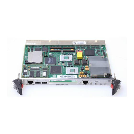
Motorola CPCI-6020 Installation And Use Manual (170 pages)
CompactPCI Single Board Computer
Brand:
Motorola
| Category:
Motherboard
| Size: 1.08 MB
Table of Contents
Table of Contents
4
About this Manual
14
Safety Notes
20
Sicherheitshinweise
26
1 Introduction
32
Features
32
Table 1-1 Features
32
Standard Compliances
33
Table 1-2 Board Standard Compliances
33
Ordering Information
34
Supported Board Models
34
Board Accessories
35
2 Hardware Preparation and Installation
36
Overview
36
Unpacking and Inspecting the Board
36
Overview of Start-Up Procedure
37
Table 2-1 Startup Overview
37
Table A-2 Manufacturers' Documents
37
Equipment Required
38
Environmental and Power Requirements
38
Environmental Requirements
38
Table 2-2 Specifications
39
Power Requirements
40
Thermal Requirements
40
Hardware Configuration
40
Table 2-3 Baseboard and RTM Power Requirements
40
CPCI-6020 Baseboard Preparation
41
Jumper Settings
42
Flash Bank Selection
42
Figure 2-1 Header Locations and Jumper Settings
42
Harrier Power up Configuration Header
43
PMC 66 Mhz Disable
43
Enable/Disable +12 V and -12 V Use
43
Enable/Disable Lockdown of One or more Flash Blocks for Bank a
44
Enable Write-Protect for Entire Flash on Bank a
44
Remote Switch
44
Hardware Installation
44
PMC Module Installation
45
Compactflash Memory Card Installation
47
Before You Install or Remove a Board
48
Watch for Bent Pins or Other Damage
49
Use Caution When Installing or Removing Boards
49
Understanding Hot Swap
49
Recognize Different Injector/Ejector Lever Types
50
Figure 2-2 Injector/Ejector Lever Types
50
Verify Slot Usage
51
Preserve EMI Compliance
51
Table 2-4 Slot Usage Indicators
51
Installing and Removing a Module
52
Startup and Operation
55
System Considerations
56
Figure 2-3 Start up Flow Diagram
56
3 Controls, Leds, and Connectors
58
Overview
58
CPCI-6020 Baseboard Layout
58
Figure 3-1 Headers, Connectors and Leds
58
Front Panel Connectors and Leds
59
Front Panel Ethernet Port
59
Table 3-1 Ethernet Connector Pin Assignments
59
Figure 3-2 Front Panel Connectors and Leds
59
Front Panel Asynchronous Serial Port
60
Front Panel USB Ports
60
Table 3-2 COM1 Pin Assignments
60
Table 3-3 USB Port 1
60
ABORT# Switch
61
RESET# Switch
61
Front Panel Leds
61
Connector Pin Assignments
61
Compactpci Bus Connectors
61
Table 3-4 USB Port 0
61
Table 3-5 Front Panel Leds
61
Table 3-6 J1 Compactpci Connector
62
Table 3-7 J2 Compactpci Connector
62
Compactpci User I/O Connector
64
Table 3-8 J3 Compactpci User I/O Connector
64
Table 3-9 Signal Descriptions for the J3 Connector
64
Compactpci User I/O Connector
65
Table 3-10 J4 Local PCI Expansion Connector Pinout
65
Compactpci User I/O Connector
66
Table 3-11 J5 User I/O Connector
66
Table 3-12 J5 Signal Descriptions
66
Memory Mezzanine Connectors
68
Table 3-13 J8 and J27 Memory Mezzanine Connector
68
PCI Mezzanine Card (PMC) Connectors
69
Table 3-14 PMC Connector J11 Pin Assignments
69
Table 3-15 J12 PMC Connector J12 Pin Assignments
70
Table 3-16 PMC Connector J13 Pin Assignments
71
Table 3-17 PMC Connector J14 Pin Assignments
72
Lock down Flash Enable Jumper
73
Table 3-18 J17 Lock down Flash Enable Jumper
73
PMC 66 Mhz Disable Jumper
74
Remote Switch Connector
74
Flash Write Protect Enable Jumper
74
Table 3-19 J21 PMC 66 Mhz Disable Jumper
74
Table 3-20 J19 Remote Switch Connector
74
Table 3-21 J20 Flash Write Protect Enable Jumper
74
Harrier Power up Configuration
75
Xport Flash Bank Select Header
75
Riscwatch Header
75
Table 3-22 J22 Harrier Power up Configuration Header Pin Assignments
75
Table 3-23 J24 Xport Flash Bank Select Header
75
Table 3-24 J25 Riscwatch Header Pin Assignments
75
Mictor Debug Connector
76
Table 3-25 J28 Debug Connector
76
4 Functional Description
82
Overview
82
Block Diagram
83
Figure 4-1 Block Diagram
83
Local PCI Bus Resources
84
PCI Bus a Resources
84
Local Compactpci Bus
84
Remote (Expansion) Compactpci Bus
84
Primary Ethernet Channel
84
ISA Bridge, Including EIDE Function
85
EIDE Interface
85
ISA Bus Resources
85
Synchronous Serial Ports
85
USB Controller
86
PCI Bus B Resources
86
PMC Slot
86
Secondary Ethernet Channel
87
Table 4-1 Special Function Processor PMC Pins
87
Processor Bus Resources
88
Processor
88
L2 Cache
88
Harrier System Memory Controller and PCI Host Bridge ASIC
88
Dual Harrier Assignments
89
Harrier Power-Up Configuration
89
Table 4-2 Harrier Power-Up Configuration Settings
89
Debug Connector
91
PPC Bus Arbitration
91
ECC Memory Bus Resources
91
Harrier a Memory Bus
91
Harrier B Memory Bus
92
RAM500 Memory Mezzanine
92
Harrier Xport Resources
92
Table 4-3 Expansion SDRAM Memory Mezzanine Size Options
92
Harrier A, Channel 0 - Onboard Bank a Flash
93
Harrier A, Channel 1 - Socketed Bank B Flash
93
Harrier A, Channel 2 - NVRAM, RTC, External Register Set
93
Harrier A, Channel 3
93
Harrier B, Channel 0, 1, 2 and 3
93
Table 4-4 Bank a Flash Options
93
Other Harrier Resources
94
I2C Bus Resources - Serial EEPROM
94
Asynchronous Serial Ports
94
32-Bit Timers
94
Watchdog Timers
94
Other Board Resources
95
Miscellaneous Control and Status
95
Clock Generator
95
Table 4-5 PPC to PCI Clock Ratios
95
Onboard Power Supplies
96
Board Reset Logic
96
Table 4-6 Reset Sources and Devices Affected
97
Figure 4-2 Reset Block Diagram
97
Soft Reset
98
Front Panel Resources
98
ABORT# and RESET# Switches
98
On-Board Leds
99
Harrier Power up Configuration Header
99
Hot Swap Support
99
High Availability Support
99
HSC Bridge Board Interface
99
Local Compactpci Bus Interface
100
Secondary Bus Arbitration
100
Secondary Bus Tri-Stating
100
System Slot Hot Swap
100
EIDE Interface
101
Ethernet Interface
101
Hot Swap Support
101
PMC Interface Module (PIM)
101
Asynchronous Serial Ports
102
Synchronous Serial Ports
102
I/O Signal Multiplexing (IOMUX)
102
Figure 4-3 Serial Port Signal Multiplexing
102
Table 4-7 Multiplexing Sequence of the IOMX Function
103
Serial Interface Modules (SIM)
104
PMC Interface Module (PIM)
104
Figure 4-4 P2MX Signal Timings
104
PMC Interface Module Form Factor
105
Figure 4-5 PMC Interface Module Layout
105
PMC Interface Connector
106
Host I/O Connector
106
Speaker Port
106
Floppy Disk Port
106
Mouse and Keyboard Port
106
5 Firmware
108
Ppcbug Overview
108
Ppcbug Basics
108
Memory Requirements
109
Ppcbug Implementation
109
MPU, Hardware and Firmware Initialization
109
Using Ppcbug
111
Debugger Commands
111
Table 5-1 Debugger Commands
112
Diagnostic Tests
115
Table 5-2 Diagnostic Test Groups
116
6 RAM500 Memory Expansion Module
118
Overview
118
RAM500 Description
118
RAM500 Module Installation
119
Table 6-1 RAM500 SDRAM Memory Size Options
119
Features
120
Srom
120
Table 6-2 RAM500 Feature Summary
120
Host Clock Logic
121
Serial Presence Detect (SPD) Data
121
RAM500 Connectors
121
Bottom Side Memory Expansion Connector (P1)
121
Table 6-3 RAM500 Bottom Side Connector (P1) Pin Assignments
121
Top Side Memory Expansion Connector (J1)
124
Table 6-4 RAM500 Top Side Connector (J1) Pin Assignments
124
RAM500 Programming Issues
126
7 Transition Module Preparation and Installation
128
Overview
128
General Description
128
Figure 7-1 Block Diagram
129
Component Layout
130
Figure 7-2 Component Layout
130
Figure 7-3 Rear Panel Connectors, Cut-Outs
131
Rear Panel Connectors
131
Unpacking and Inspecting the RTM
132
Preparing the Transition Module
132
Serial Ports 1 and 2
132
Serial Ports 3 and 4
133
Table 7-1 SIM Model Numbers
133
Serial Interface Module Circuitry
134
Figure 7-4 Ports 3 and 4 Header Settings
134
Port Configuration
136
Figure 7-5 EIA-232-D DCE Ports 3 and 4 Configuration
136
Installing the Sims
137
Figure 7-6 EIA-232-D DTE Ports 3 and 4 Configuration
137
Installing the PIM
139
Installing and Removing the Transition Module
141
Connectors and Cables
142
Table 7-2 Rear Transition Module Connectors/Headers
142
Table 7-3 Rear Transition Module Cables
143
Connector Pin Assignments
144
Compactpci Connectors
144
PMC I/O Module Connector
144
Table 7-4 PMC I/O Module - Host I/O Connector Pin Assignments
144
Table 7-5 PMC I/O Module - PMC I/O Connector Pin Assignments
145
10Baset/100Basetx Connectors
147
COM1 Connector
147
Table 7-6 10Baset/100Basetx Connector Pin Assignments
147
Table 7-7 COM1 Connector Pin Assignments
147
COM2 Header
148
EIDE Header
148
Table 7-8 COM2 Header Pin Assignments
148
Table 7-9 EIDE Header Pin Assignments
148
Floppy Port Header
149
5VDC Power Connector
149
Table 7-10 Floppy Header Pin Assignments
149
Table 7-11 +5Vdc Power Connector
149
Keyboard/Mouse Connector
150
Sync/Async Serial Ports
150
Table 7-12 Keyboard/Mouse Connector Pin Assignments
150
Table 7-13 Sync/Async Serial Connector Pin Assignments
150
Speaker Output Header
151
Table 7-14 Speaker Output Connector Pin Assignments
151
8 CNFG and ENV Commands
152
Overview
152
CNFG - Configure Board Information
152
ENV - Set Environment
153
Configuring the Ppcbug Parameters
153
Related Documentation
162
Embedded Communications Computing Documents
162
Manufacturers' Documents
162
Table A-1 Embedded Communications Computing Documents
162
Related Specifications
163
Advertisement
Advertisement
Related Products
Motorola CPCI-6115
Motorola CPV5000
Motorola CPV5300 CompactPCI
Motorola CPV5300TM80
Motorola CPCI-9120
Motorola CP150
Motorola CPEI 890
Motorola CPEI 25150
Motorola CP110 VHF
Motorola CPEi 35825
Motorola Categories
Cell Phone
Two-Way Radio
Baby Monitor
Cordless Telephone
Radio
More Motorola Manuals
Login
Sign In
OR
Sign in with Facebook
Sign in with Google
Upload manual
Upload from disk
Upload from URL