Philips HTB3560/12 Service Manual
Home theater bd player
Hide thumbs
Also See for HTB3560/12:
- Quick manual (3 pages) ,
- Quick manual (3 pages) ,
- Quick start manual (8 pages)
Table of Contents
Advertisement
Home Theater BD Player
Service
Service Manual
. Location of PCB Boards,Version Variation and Repair Scenario Matrix....1-2
. Technical Specifications.........................................................1- 3
. Safety Instruction, Warning & Notes........................................1- 4
. DFU Instruction..............................................................................2-1
. Mechanical and Dismantling Instructions....................................3-1
. Software Upgrades .......................................................................
. Trouble Shooting Chart......................................................
. Wiring Diagram..................................................................6-1
. Electrical Diagrams and Print-layouts......................................7-1
. Votages and Waveforms for Connection Pins...........................8-1
. Pin Description & Block Diagrams of ICs..................................9-1
. Set Mechanical Exploded view & Part list...............................10-1
. Revision List.................................................................................11-1
©Copyright 2011 Philips Consumer Electronics B.V. Eindhoven, The Netherlands
All rights reserved. No part of this publication may be reproduced, stored in aretrieval system or
transmitted, in any form or by any means, electronic, mechanical, photocopying, or otherwise
without the prior permission of Philips.
Published by Arya & Stephen - 1246 BU AVM Printed in The Netherlands Subject to modification
Version 1.3
TABLE OF CONTENTS
HTB3560/12/78 K/98/94/40/55
Page
4-1
.
5-1
.
PHILIPS
CLASS 1
LASER PRODUCT
3141 785 38343
GB
Advertisement
Table of Contents

Related Manuals for Philips HTB3560/12


Summary of Contents for Philips HTB3560/12
-
Page 1: Table Of Contents
. Set Mechanical Exploded view & Part list.…………………..….…10-1 . Revision List.................11-1 CLASS 1 ©Copyright 2011 Philips Consumer Electronics B.V. Eindhoven, The Netherlands All rights reserved. No part of this publication may be reproduced, stored in aretrieval system or LASER PRODUCT transmitted, in any form or by any means, electronic, mechanical, photocopying, or otherwise without the prior permission of Philips. - Page 2 PCB BOARD LOCATION: AMPLIFIER BOARD MAIN BOARD LOADER POWER BOARD FRONT CONTROL BOARD VERSION VARIATIONS Type / Versions HTB3560 Service Police K/98 Board in used MAIN BOARD FRONT CONTROL BOARD M +C M +C M +C M +C M +C POWER BOARD M +C M +C...
- Page 3 Production Specifications: File formats Audio: .aac, .mka, .mp3, .wma, .wav Video: .avi, .divx, .mp4, .mkv, .mpg, .mpeg, .rmvb, .rm Picture: .jpg, .jpeg, .gif, .png Note notice. Total output power: 300W RMS (30% THD) Frequency response: 20 Hz-20 kHz / Region codes ±3 dB Signal-to-noise ratio: >...
-
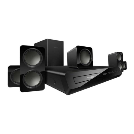
Page 4: Main Unit
Rear speaker: Output power: 2 x 50 W RMS (30% THD) Compatibility: Hi-Speed USB (2.0) Speaker impedance: 4 ohm Class support: USB Mass Storage Class Speaker drivers: 1 x 63.5 mm (2.5") woofer (MSC) Dimensions (WxHxD): 84.5 x 89 x 89 mm File system: FAT16, FAT32, NTFS Maximum memory support: <... -
Page 5: Safety Instruction, Warning & Notes
Safety instruction, Warning & Notes Safety instruction 1. General safety 2.Laser safety Safety regulations require that during a repair: This unit employs a laser. Only qualified service personnel . Connect the unit to the mains via an isolation transformer. may remove the cover, or attempt to service this device . - Page 6 Warning 1.General 2. Laser . All ICs and many other semiconductors are susceptible to . The use of optical instruments with this product, will electrostatic discharges (ESD). Careless handing during increase eye hazard. repair can reduce life drastically. Make sure that, during .
- Page 7 Solder Joint...
- Page 8 - lead free BGA-ICs will be delivered in so-called respected by the workshop during a repair: ‘dry-packaging’ (sealed pack including a silica gel Use only lead-free solder alloy Philips SAC305 with pack) to protect the IC against moisture. After order code 0622 149 00106. If lead-free solder-paste is...
- Page 9 EN Before using your product, read all accompanying safety information MS Sebelum menggunakan produk anda, baca semua maklumat keselamatan yang disertakan User manual Power Cord HDMI...
- Page 10 EN Connect the home theater MS Sambungkan teater rumah FRONT FRONT FRONT WOOFER LEFT RIGHT CENTER STS3001 FRONT FRONT FRONT REAR REAR RIGHT LEFT CENTER RIGHT LEFT WOOFER REAR REAR LEFT RIGHT FRONT FRONT FRONT REAR REAR RIGHT LEFT RIGHT LEFT WOOFER CENTER...
- Page 11 HDMI OUT (ARC) HDMI (ARC) / HDMI IN AC MAINS~...
- Page 12 EN Switch on the home theater MS Hidupkan teater rumah...
- Page 13 EN Co MS Lengkapkan persediaan kali pertama HDMI HOME THEATER HOME THEATER...
- Page 14 EN Use your home theater MS Gunakan teater rumah anda...
- Page 15 MUSIC iLINK...
-
Page 16: Remote Control
Remote control This section includes an overview of the remote control. Congratulations on your purchase, and of product software upgrade), register your product at www.philips.com/welcome. Main unit This section includes an overview of the main unit. a Disc compartment b Display panel... -
Page 17: Open Or Close The Disc Compartment, Or
+/- (Volume) (Standby-On) Increase or decrease volume. Switch the home theater on or to standby. SOUND SETTINGS When EasyLink is enabled, press Access or exit sound options. and hold for at least three seconds l Alphanumeric buttons to switch all connected HDMI CEC Enter values or letters (using SMS style compliant devices to standby. -
Page 18: Mechanical And Dismantling Instructions
Mechanical and Dismantling Instructions Dismantling Instruction Detailed information please refer to the model set. The following guidelines show how to dismantle the player. Step1: Remove 6 screws around the Top Cover, and then remove the Top Cover (Figure 1). Figure 1 Step2: If it is necessary to dismantle Loader or Front Panel, the Front door should be removed first. - Page 19 Mechanical and Dismantling Instructions Detailed information please refer to the model set. Dismantling Instruction :Dismantle Front Panel, disconnect the connectors (XS604, XP12), need release 2 snaps of Front Panel & 2 snaps Step3 of bottom cabinet , then gently pull the Panel out from the set. (Figure 3) Figure 3 Step4 : Dismantle Front Control Board,remove 5 screws (Figure 4...
- Page 20 Mechanical and Dismantling Instructions Dismantling Instruction Detailed information please refer to the model set. : Dismantle Main Board, first disconnect 2 connectors (XP1, XP11), and then remove 5 screws. (Figure 5/6) Step6 : Dismantle Power Board, disconnect the connector s XP502 and CN502 on Power Board,then remove 5 screws.(Figure 5/6) Step7 (Figure 5/6) Step8: Dismantle Amplifier Board, remove...
-
Page 21: Software Upgrades
2. Check the version information after upgraded. Press the Home key on RC , select ‘Setup’‐>’Advanced’‐>’Version information’ in order, and then press OK Key you will see a interface like below: Model:HTB3560/78 Version SystemSW:x.xx.xx Subsystem SW:xx‐xx‐xx‐xx Ethernet MAC:xx:xx:xx:xx:xx:xx EUI64:xx xx xx xx xx xx xx xx For information,frequently asked question and software updates,visit www.philips.com/support. Close ... -
Page 22: Trouble Shooting Chart
Trouble shooting Chart VFD No display on Front Control Board VFD No display on Front Control Board Check every supply voltage on Main Board whether normal or not. Refer to XP501 on Power Board (XP9, PIN6: +5V, PIN5: 12V) Check voltage +5V,+12V on Power Fix the connection XP3 on Front... - Page 23 Trouble shooting Chart keys do not work keys do not work Check voltage +5V on Front Board U301 Fix the connection XP3 to XP9 on Main PIN7、PIN21 Board Check Front Control Board signals at XP3 Pin8 VSCLK, Pin7 VSDA,Pin6 VSTB Replace U8 on Main Board, or replace Main Board Replace U301 on Front Board...
- Page 24 Trouble shooting Chart Remote control does not work Remote control does not work Check battery of remote control whether exhausted or not. Replace the battery for remote control Check power supply of IR601 on Front Check the +5V net on Front Control Control Board whether normal or not Board to Main Board XP9 XP3 Pin9 :+5V...
- Page 25 Trouble shooting Chart No audio output No audio output Check XP13 Pin 14&16 3.3V on Main Check voltage +35.5V (35.5V Board whether normal or not HTB3560/78) for whether normal or not at on Amplifier Board Refer to XP501 on Power Board Check the 24Pin FFC connection XP13 on Main Board and XP701 on Amplifier Board whether right or not between Main Board...
- Page 26 Trouble shooting Chart No video output No video output Check L452, R616 whether right on Main Board Add L452, R616 Check the video signal whether right at U1: PIN B18 or R615 Replace Main IC or Main Board...
- Page 27 Trouble shooting Chart Can’t read disc or can’t open the disk door Can’t read disc or can’t open the disk door Check loader work normally or not Check XP7 on Main Board Check 45Pin, 8Pin, 4Pin cable from Main Board to Loader connect right or Fix 45Pin, 8Pin, 4Pin cable Replace Loader 、...
- Page 28 Trouble shooting Chart Tuner FM does not work Tuner FM does not work Check voltage at Q28 C electrode (+5V) on Main Board whether normal Refer to Power Board XP501 or not Check voltage +3.3V Tuner module (TUN1 Pin8) whether right or Check Main Board tuner power supply circuit.
- Page 29 Trouble shooting Chart AUX in does not work AUX in does not work Check voltage at U18 PIN16:5V on Main Board whether normal or not Refer to Power Board XP501 Check Main Board U18 Pin4, Pin11 signal input whether right or not Check AUX IN connector Check 74HC4052...
- Page 30 Trouble shooting Chart MP3 Link does not work MP3 Link does not work Check signal JACK602 PIN3:MP3_R PIN2:MP3_L ON front board whether normal or Refer to Main Board XP604 Check Main Board U18 74HC4052 PIN2, Check Main Board C278, C279, R352, PIN15 L/R signal input right or not R458, Check voltage at U18 74HC4052...
- Page 31 5-10 Trouble shooting Chart COAX in does not work COAX in does not work Check voltage at U27 PIN6/PIN23:3.3V on Main Board whether normal or not Refer to Power Board XP501 Check Main Board U27 CS8416 PIN2 input signal whether normal or not Check Main Board C360,L11 Check U27 CS8416 whether broken.
- Page 32 5-11 Trouble shooting Chart Network in does not work Network in does not work P1 Pin2, Pin3, Pin5, Pin6 from Check netting twine normal or not netting twine link Check normal or Replace P1...
- Page 33 HTB3560/12/K98/94/40/55 BD HTS 300W (Equal)30%THD Block Diagram Draft Follow design ASA LOADER DDR3 NAND L9829B SANYO WIFI 1Gb+2Gb 415H09 OPU NEW design DRIVER TPIC2050 RJ45 ARC IN 50WX34R) 30% 50WX34R) 30% CS8416 OPTI IN CVBS Output STA518 MIC IN HDMI Output...
- Page 34 HTB3560/78 BD HTS400W (Equal)30%THD Block Diagram Draft ASA 9829+ DDR3 NAND SANY0 414H08 WIFI 1Gb+2Gb DRIVER TPIC2050 RJ45 ARC IN 68WX34R) 30% CS8416 OPTI IN CVBS Output STA516B 4558 HDMI Output STA309 DIR I2S AUX IN 50WX6(4R) 30% AUDIO Controls MPEG Decoder 74HC405 MTK8560...
- Page 35 Front Board Circuit Diagram : 14PIN/1.0mm 14PIN/1.0mm MO_5V R316 R316 NC/33 NC/33 LED- +12V R694 R694 R637 R637 VSCLK R703 R703 R704 R704 R705 R705 R641 R641 VSDA 4.7K 4.7K 4.7K 4.7K 4.7K 4.7K R639 R639 VSTB U301 U301 GRID[1:7] DRIVER_LED_ET6202 DRIVER_LED_ET6202 KEY_POW...
- Page 36 Power Board Circuit Diagram for HTB3560/12/K98/94/40/55: R540A R540A CY506 CY506 XP502 4PIN/2.5mm XP502 4PIN/2.5mm C533 C533 1500pF/1KV 1500pF/1KV R575 R575 Q571 Q571 R540B R540B 470pF/250VAC 470pF/250VAC PNP_MMBT8550CLT1 PNP_MMBT8550CLT1 M+5V R540C R540C T531 T531 PQ3230 PQ3230 R578 R578 Alternative L531 L531...
- Page 37 Power Board Circuit Diagram for HTB3560/78: R540A R540A CY506 CY506 XP502 4PIN/2.5mm XP502 4PIN/2.5mm C533 C533 1500pF/1KV 1500pF/1KV R575 R575 Q571 Q571 R540B R540B 100pF/250VAC 100pF/250VAC PNP_MMBT8550CLT1 PNP_MMBT8550CLT1 M+5V R540C R540C T531 T531 PQ3230 PQ3230 R578 R578 Alternative D533 D533 10A/200V 10A/200V L531...
- Page 38 Amplifier Board Circuit Diagram for HTB3560/12/K98/94/40/55:STA309A VD3.3V R800 R800 0/NC 0/NC D705 D705 Q702 Q702 LL4148 LL4148 PNP_MMBT8550CLT1 PNP_MMBT8550CLT1 VD3.3V R739 R739 C716 C716 0.1uF/25V/Y5V 0.1uF/25V/Y5V CE723 CE723 47uF/50V 47uF/50V ASDAT0 LRCLK TP41 TP41 R805 R805 Q701 Q701 D712 D712...
- Page 39 Amplifier Board Circuit Diagram for HTB3560/12/K98/94/40/55:STA518 L708 L708 10uH/5A 10uH/5A U701 U701 IC_36P_STA518 IC_36P_STA518 TP26 TP26 SUB- TP27 TP27 SUB+ VCC-Sign SUB-GND L702 L702 22uH/3.3A/NC 22uH/3.3A/NC TP28 TP28 TP29 TP29 VCC-Sign OUT2B C734 C734 C735 C735 TP30 TP30 TP31 TP31 0.1uF/50V/X7R...
- Page 40 Amplifier Board Circuit Diagram for HTB3560/78:STA309A D705 D705 +12V Q702 Q702 LL4148 LL4148 PNP_MMBT8550CLT1 PNP_MMBT8550CLT1 VD3.3V R739 R739 C716 C716 R805 R805 CE723 CE723 0.1uF/25V/Y5V 0.1uF/25V/Y5V 100uF/16V 100uF/16V TP41 TP41 D712 D712 LL4148 LL4148 ASDAT0 R710 R710 LRCLK Q701 Q701 AM_MUTE C714 C714...
- Page 41 Amplifier Board Circuit Diagram for HTB3560/78:STA518 C471 C471 C472 C472 C473 C473 C474 C474 C453 C453 C452 C452 0.1uF/50V/X7R 0.1uF/50V/X7R 0.1uF/50V/X7R 0.1uF/50V/X7R U701 U701 TP26 TP26 SUB- STA516B STA516B TP27 TP27 SUB+ TP28 TP28 VCC-Sign SUB-GND TP29 TP29 C734 C734 C735 C735 L702...
- Page 42 Front Control Board Print-layout (top side):...
- Page 43 Power Supply Print-layout (top side) for HTB3560/12/K98/94/40/55:...
- Page 44 7-10 7-10 Power Supply Print-layout (top side) for HTB3560/78:...
- Page 45 7-11 7-11 Amplifier Board Print-layout (top side) for HTB3560/12/K98/94/40/55:...
- Page 46 7-12 7-12 Amplifier Board Print-layout (bottom side) for HTB3560/12/K98/94/40/55:...
- Page 47 7-13 7-13 Amplifier Board Print-layout (top side) for HTB3560/78:...
- Page 48 7-14 7-14 Amplifier Board Print-layout (bottom side) for htb3560/78:...
- Page 49 Voltages for per connection pin XP9--From Main Board Connect to Front Board XP13--From Main Board Connect to Amp Board XP1--From Main Board Connect to Power Board Pin No Pin Assin Remarks Pin No Pin Assin Remarks Pin No Pin Assin Remarks Reserved DATA0...
- Page 50 Waveforms for measure point XP13 Pin20_POWER_derating XP13 Pin12_ AMP MUTE XP13 P13_AMP RST XP13 P9_ AMP SCL XP13 Pin7_AOMCLK XP13 Pin10 _AMP SDA XP13 Pin5_AOBCK XP13 Pin4_AOSDATA2...
- Page 51 Waveforms for measure point XP13 Pin1_AOSDATA0 XP13 Pin3_AOSDATA1 XP13 Pin2 _AOLRCK XP13 Pin23 _PDWN XP13 Pin22 _TH_WAR...
- Page 52 U1 Main IC-MT8560_BAAG Functional Block Diagram NAND DDR3 256/384MB Audio 7.1 CH 2 CH MT8560 S/PDIF Motor Driver HDMI HD+SD Decode Component 810MHz ARM11 Ethernet CVBS 400MHz AudioDSPx3 HDMI 1.4 Ethernet...
- Page 53 U1 Main IC-MT8560_BAAG Pin Assignment...
- Page 54 U409 Motor Drivers IC‐ TPIC2050 1. Block Diagram ...
- Page 55 2. Pin assignment ...
- Page 56 3. Pins definition ...
- Page 57 U26 Audio A/D IC ‐AK5358K 1. Block diagram ...
- Page 58 3. Pin Function ...
- Page 59 U531 Internal IC Diagram-TNY179EN on Power Board:...
- Page 60 U534 Internal IC Diagram-TOP260EN on Power Board:...
- Page 61 9-10 9-10 U534 IC TOP258EN Diagram on Power Board:...
- Page 62 10-1 Exploded View of HTB3560/12 /78 K/98 /94/40/55:...
-
Page 63: Revision List
11-1 REVISION LIST Version 1.0 * Initial release for HTB3560/12/78 Version 1.1 * Initial release for HTB3560K / 98 Version 1.2 * Initial release for HTB3560/94 Version 1.3 * Initial release for HTB3560/40/55...