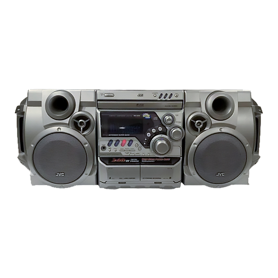
JVC MX-G50 Service Manual
Compact component system
Hide thumbs
Also See for MX-G50:
- Instructions manual (28 pages) ,
- Instructions for use manual (28 pages)
Table of Contents
Advertisement
SERVICE MANUAL
COMPACT COMPONENT SYSTEM
MX-G50 / MX-G56
STANDBY/ON
1
2
3
SUBWOOFER
SLEEP
LEVEL
4
5
6
SOUND
AUX
MODE
7
8
9
FM MODE
10
+10
FADE
FM/AM
TAPE
TAPE A/B
MUTING
CD
DISC SKIP
/
+
VOLUME
VOLUME
Ð
RMÐSMXG50A REMOTE CONTROL
Each difference points
CD/DECK/
MODEL
RECEIVER
MX-G50 J
CA-MXG50
MX-G50 C
CA-MXG50
MX-G56 C
CA-MXG56
Contents
Safety Precautions
Important for laser products
Preventing static electricity
Disassembly method
Wiring connection
Adjustment method
STANDBY
STANDBY/ON
COMPACT COMPONENT SYSTEM
PHONES
CLOCK
/ TIMER
DISPLAY
REPEAT
PROGRAM
REC START
/STOP
COMPU PLAY CONTROL
EJECT
A
PLAY
FULL - LOGIC CONTROL
SP-MXG50
CA-MXG50
Optical
Speaker
POWER / SUB / CD EJECT /
out
DISK CHANGER button
SP-MXG50
SP-MXG50
METALLIC LIGHT GRAY
SP-MXG56
1-2
1-3
1-4
1-5
1-20
1-21
COPYRIGHT
2001 VICTOR COMPANY OF JAPAN, LTD.
DISC CHANGE
CD-R / RW PLAYBACK
PLAY & EXCHANGE
MX-G50
SOUND
MODE
COMPACT
DIGITAL AUDIO
SUBWOOFER
LEVEL
PRESET
SET
CANCEL
/DEMO
TUNING
RANDOM
CD
REC START
DUBBING
TAPE A
TAPE B
EJECT
B
CD SYNCHRO RECORDING
REC/PLAY
SP-MXG50
Color
VOLUME RING
SILVER
SILVER
Flow of functional operation
until TOC read
Maintenance of laser pickup
Replacement of laser pickup
Trouble shooting
Description of major ICs
MX-G50/MX-G56
MX-G50
Area Suffix
J
U.S.A.
C
Canada
MX-G56
Area Suffix
C
Canada
CD fitting
ornament
1-25
1-26
1-26
1-27
1-30
No.20913
Feb. 2001
Advertisement
Table of Contents

Related Manuals for JVC MX-G50


Summary of Contents for JVC MX-G50
- Page 1 MX-G50/MX-G56 SERVICE MANUAL COMPACT COMPONENT SYSTEM MX-G50 MX-G50 / MX-G56 Area Suffix U.S.A. Canada MX-G56 Area Suffix Canada DISC CHANGE STANDBY STANDBY/ON CD-R / RW PLAYBACK PLAY & EXCHANGE COMPACT COMPONENT SYSTEM MX-G50 SOUND MODE COMPACT STANDBY/ON DIGITAL AUDIO SUBWOOFER...
-
Page 2: Safety Precautions
MX-G50/MX-G56 Safety Precautions 1. This design of this product contains special hardware and many circuits and components specially for safety purposes. For continued protection, no changes should be made to the original design unless authorized in writing by the manufacturer. -
Page 3: Important For Laser Products
MX-G50/MX-G56 Important for laser products 5.CAUTION : If safety switches malfunction, the laser is able 1.CLASS 1 LASER PRODUCT to function. 2.DANGER : Invisible laser radiation when open and inter 6.CAUTION : Use of controls, adjustments or performance of lock failed or defeated. Avoid direct exposure to beam. -
Page 4: Preventing Static Electricity
MX-G50/MX-G56 Preventing static electricity 1. Grounding to prevent damage by static electricity Electrostatic discharge (ESD), which occurs when static electricity stored in the body, fabric, etc. is discharged, can destroy the laser diode in the traverse unit (optical pickup). Take care to prevent this when performing repairs. -
Page 5: Disassembly Method
Optical out Remove the six screws B attaching the metal cover only on both sides of the body. MX-G50 J MX-G56 C Remove the metal cover from the body by lifting the rear part of the cover. ATTENTION: Do not break the front panel tab fitted Fig.1... - Page 6 MX-G50/MX-G56 Removing the CD Tray fitting (1) OPEN/CLOSE button CD tray (See Fig. 4 to 6) POWER button Prior to performing the following procedure, remove the metal cover. Press the POWER button. Press the OPEN/CLOSE button to eject the CD tray.
- Page 7 MX-G50/MX-G56 Removing the CD changer unit CD servo board CD changer unit (See Fig.8 to 10) CW105 Prior to performing the following procedure, remove the metal cover. Disconnect the card wire which is attached with adhesive to the left side of the CD changer unit.
- Page 8 MX-G50/MX-G56 Removing the front panel assembly Front panel assembly (See Fig.11 to 13) FCW3 Main board JCW2 Prior to performing the following procedure, remove JCW1 the metal cover and the CD changer unit. ACW1 Disconnect the card wire from connector FCW3 and...
-
Page 9: Removing The Rear Cover
CD changer unit, heat sink & AMP Main board board and tuner pack. CON01 Remove the fore screws M and one screw M' (Only MX-G50 J / MX-G56 C) attaching the rear panel. Optical out only MX-G50 J Tuner board MX-G56 C Fig.16... -
Page 10: Removing The Mainboard
MX-G50/MX-G56 Removing the main Board (See Fig. 18) FCW3 Prior to performing the following procedure, remove JCW2 the metal cover, CD changer unit, heat sink & AMP JCW1 board tuner pack and rear cover. HCW3 PCW1 Disconnect the card wire from connector FCW3 and... - Page 11 MX-G50/MX-G56 <Front panel assembly> Power / CD switch board Tab e Prior to performing the following procedure, remove the metal cover, the CD changer unit and the front panel assembly. UCW2 FLdiplay & system Removing the power / CD switch board...
- Page 12 MX-G50/MX-G56 <CD changer unit> Prior to performing the following procedure, remove the CD changer unit. Removing the CD tray (See Fig.25 to 27) Turn the black loading pulley gear on the under side of the CD changer unit in the direction of the arrow and draw the CD tray toward the front until it stops.
- Page 13 MX-G50/MX-G56 Removing the sensor board / the turn table motor assembly (See Fig.30 to 32) Prior to performing the following procedure, remove the CD tray. Remove the screw X attaching the sensor board and release the two tabs h attaching the sensor board on the under side of the CD tray.
- Page 14 MX-G50/MX-G56 Removing the belt, the CD servo board and the switch board (See Fig.33 and 34) Belt Prior to performing the following procedure, remove the CD tray. Detach the belt from the pulley on the upper side of the CD changer unit (Do not stain the belt with grease).
- Page 15 MX-G50/MX-G56 Removing the CD mechanism holder assembly (mechanism included) Motor connecter (See Fig.35 to 38) Disconnect the harness from connector on the CD mechanism board in the CD mechanism assembly on the under side of the CD changer unit. Disconnect the card wire from the pickup unit connector.
-
Page 16: Removing The Pickup Unit
MX-G50/MX-G56 <CD mechanism section> Shaft Shutter Pickup unit • Removing the CD mechanism holder from the CD chager unit. (Refer to "Removing the CD mechanism holder assembly" ) Removing the pickup unit. ( See Fig.1) 1. Removing the cut washer c on the feed gear sleeve and pull out the feed gear. -
Page 17: Cassette Mechanism Section
MX-G50/MX-G56 R/P Head <Cassette mechanism section> Removing the record/playback mechanism. Removing the R/P head. 1. Remove the screw A on the right side of the R/P head.(Fig.1, Fig.2) 2. Remove the screw B on the left side of the R/P head.(Fig.1, Fig.2) Remove the erase head. -
Page 18: Removing The Motor
MX-G50/MX-G56 Motor Mecha. terminal board Removing the motor. 1. Remove the two screws D fixing the motor. Be careful to grease's splash when the drive belt comes off.(Fig.5, Fig.6) 2. Unsolder the motor terminal.(Fig.5) Removing the mechanism board. Unsolder the four parts a on the solenoid... -
Page 19: Removing The Side Panel
MX-G50/MX-G56 < Speaker section > Side panel Removing the side panel (See Fig. 1) Remove the five screws A attaching the side panel, then remove the side panel. Fig.1 Side speaker Removing the side speaker (See Fig. 2 and 3) -
Page 20: Wiring Connection
MX-G50/MX-G56 Wiring connection Color codes are shown below. Brown Orange Yellow Green Blue Violet Gray White Black 1-20... -
Page 21: Adjustment Method
MX-G50/MX-G56 Adjustment method 1. Tuner * Adjustment Location of Tuner PCB LW OSC AM(MW) RF AM(MW) RF AM(MW) OSC Adjustment Adjustment Adjustment Adjustment ITEAM Received FREQ. 594 KHz 146~290 KHz 150 KHz 522~1611 KHz Adjustment point Maximum Maximum 2~7.0 0.5 V 1~7.0... - Page 22 MX-G50/MX-G56 FM THD Adjustment Output Antenna SSG FREQ. Terminal 98 MHz Oscilloscope FM S.S.G Adjustment Input point FM DETECTOR COIL Speaker (FM DET) Terminal output Input 60 dB Output Distortion Meter Minumum Distortion (0.4% below) (Figure 1-1) Figure1-1 IF CENTER and THD Adjustment...
-
Page 23: Cassette Deck
MX-G50/MX-G56 2 Cassette Deck To adjust tape speed Notes Cassette Deck Frequency Counter 1) Measuring tape: i) VT-712/MTT-111(or equivalent) (Tapes recorded with 3kHz) SPK OUT ii) AC-225/MTT-5512(or equivalent) output 2) Connect the cassette deck to the frequency counter as in figure 1-5. - Page 24 MX-G50/MX-G56 To adjust plabyback level/REC -114N(or equivalent 10kHz AZIMUTH control) Notes 1) Before the actual adjustment, clean the play/recording head. 2) Measuring tape : i) VT-703 / MTT-114N(or equivalent 10kHz AZIMUTH control) ii) AC-225/MTT-5512(or equivalent) 3) The cassette deck is connections as shown in figure 1-7.
-
Page 25: Flow Of Functional Operation Until Toc Read
MX-G50/MX-G56 Flow of functional operation until TOC read Check Point Play Key Power ON RESET a CD LSI Confirm that the voltage at the pin17 of KB9226(IC101) is "L" "H". Confirm that the voltage at the pin33 LIMIT SW ON of KB9226(IC101) is "H"... -
Page 26: Maintenance Of Laser Pickup
MX-G50/MX-G56 Maintenance of laser pickup Replacement of laser pickup (1) Cleaning the pick up lens Before you replace the pick up, please try to Turn off the power switch and,disconnect the clean the lens with a alcohol soaked cotton power cord from the ac outlet. -
Page 27: Troubleshooting
MX-G50/MX-G56 Troubleshooting 1. Amplifier Power malfunction -Check the main PCB; Front PCB -com Main PCB RIC(L4959) RBD1(PBL403) RD8(IN5392) VDD(5V) normal? pin no.2, 10 input -Check the power PCB; UIC1 pin no.18, 46,90 voltage normal? Fuse P/T, RFS2, RFS5, RFS6 -Check the main PCB... - Page 28 MX-G50/MX-G56 2. Tuner malfunction(FM/AM) 3. Tape malfunction 1-28...
- Page 29 MX-G50/MX-G56 4. CD 1-29...
-
Page 30: Description Of Major Ics
MX-G50/MX-G56 Description of major ICs L4959 (RIC1) : Voltage regulator 1.Pin layout OUT 12V(a) OUT 8.6V EN 8.6V EN 12V(a) EN 12V(b) N.C. OUT 5.6V OUT 12V(b) TAB CONNECTED TO PIN 6 D97AU716A 2.Block diagram 2/10 5.6V, 250mA OUT 5.6V REGULATOR 8.6V, 600mA... - Page 31 MX-G50/MX-G56 BA4560 (AIC3, AIC4, AIC5, AIC6, AIC7, FIC4, HIC1, JIC2) : OP amp. 1.Pin layout OUT1 – IN1 OUT2 – + IN1 – IN2 – + IN2 KA22291(JIC1) : RB/REC PRE AMP 1.Pin layout KA22291 1 2 3 4 5 6 7 8 9 10 11 12 2.Block diagram...
-
Page 32: Pin Layout
MX-G50/MX-G56 5L9290 (IC201) : DIGITAL SIGNAL PROCESSOR FOR CDP 1. Pin layout VSSA_PLL BCKO VCO1LF LRCKO VSSD_PLL SADTO VDDD_PLL DATX VDDD1_5V C2PO S5L9290X JITB DSP+DAC XOUT SBCK 48-LQFP-0707 VSSD1_5V VDDD3-5V EFMI VSSD2-3V LOCK VDDD2-3V SMEF MUTE SMON SQDT 2. BLOCK DIAGRAM... -
Page 33: Pin Description
MX-G50/MX-G56 (1/2) 3. Pin function NAME Pin Description VSSA_PLL Analog Ground for DPLL VCO1LF Pump out for VCO1 VSSD_PLL Digital Ground Separated Bulk Bias for DPLL VDDD_PLL Digital Power Separated Bulk Bias for DPLL (3V Power) VDDD1-5V Digital Power (5V Power, I/O PAD) X'tal oscillator input (16.9344MHz) - Page 34 MX-G50/MX-G56 3. Pin function (2/2) NAME Function Description SQDT Subcode-Q data serial output MUTE System mute at 'H' VDDD2-3V Digital Power (3V Power, Internal Logic) VSSD2 Digital Ground (Internal Logic) VDDD3-5V Digital Power (5V Power, I/O PAD) SBCK Subcode data transfering bit clock...
- Page 35 MX-G50/MX-G56 M66010 (UIC2) : I/O control 1.Pin layout 2.Block diagram Shift register 1 SERIAL DATA OUTPUT D24 D23 D22 D3 D2 D1 CLOCK INPUT SET INPUT CHIP SELECT Q24 Q23 Q22 Q3 Q2 Q1 PARALLEL INPUT Parallel output latch DATA I/O...
- Page 36 MX-G50/MX-G56 KB9226 (IC101) : RF AMP & SERVO SIGNAL PROCESSOR 1. Pin layout 35 34 33 32 31 30 29 28 27 26 PDAC PDBD LOCK WDCK S1L9226X CLVI RESET DCCI DCCO MDATA VREF ISTAT 10 11 2. BLOCK DIAGRAM...
- Page 37 MX-G50/MX-G56 (1/2) 3. Pin function Pin No. Symbol Description RF summing amp. inverting input RF summing amp. output RFO DC eliminating input(use by MIRROR, FOK ,AGC & EQ terminal) RF equalizer output EFMI EFM slice input. (input impedance 47K) Main power supply...
- Page 38 MX-G50/MX-G56 3. Pin function (2/2) Pin No. Symbol Description 1-38...
- Page 39 MX-G50/MX-G56 KA9258D (IC925) : 4-ch Motor driver 28 27 26 25 24 23 22 21 20 19 18 17 16 15 REGULATOR T • S • D MUTE 10 11 12 13 14 STK402-090 (AIC2) / STK402-040 (AIC1) 1.Pin layout...
- Page 40 MX-G50/MX-G56 LC86P6548 (UIC1) : Microcontroller 1.Pin layout S48/P G0 S19/P C3 S49/P G1 S18/P C2 S50/P G2 S17/P C1 S51/P G3 S16/P C0 VDD3 S15/T15 S14/T14 S13/T13 VSS2 S12/T12 VDD2 S11/T11 S10/T10 S9/T9 S8/T8 S7/T7 P10/S O0 S6/T6 P11/S I0/SB0...
- Page 41 MX-G50/MX-G56 2.Block diagram Interrupt Control A15-A0 Standby Control D7-D0 PROM Control DASEC PROM(48KB) X’ tal Base Timer Bus Interface SIO0 Port 1 B Register C Register SIO1 Port 3 Timer 0 Port 7 Timer 1 Port 8 INT0-3 Noise Filt er...
- Page 42 MX-G50/MX-G56 LA1837 (IC01) : FM IF/DET AM RF/IF/DET 1-42...
- Page 43 MX-G50/MX-G56 TDA7442D (FIC1) : Audio processor 1.Pin layout R_IN3 R_IN4 R_IN2 LOUT R_IN1 ROUT L_IN1 AGND L_IN2 L_IN3 CREF L_IN4 MUXOUTL IN(L) DIG-GND MUXOUT(R) TREBLE(R) IN(R) TREBLE(L) BIN(R) BOUT(R) BIN(L) BOUT(L) 2.Block diagram 5.6K 5.6nF 100nF 100nF 100nF 2.2 F...
- Page 44 MX-G50/MX-G56 VICTOR COMPANY OF JAPAN, LIMITED AUDIO & COMMUNICATION BUSINESS DIVISION PERSONAL & MOBILE NETWORK BUSINESS UNIT. 10-1,1chome,Ohwatari-machi,Maebashi-city,371-8543,Japan Printed in Japan (No.20913) 200102(V)
-
Page 45: Block Diagram
MX-G50/MX-G56 Block diagram Only U version... - Page 46 MX-G50/MX-G56 Standard schematic diagrams Main section SHEET 2/5 (ONLY MX-G50 J / MX-G56 C) SHEET 2/5 MAIN signal TUNER signal CD signal TAPE P.B. signal TAPE REC. signal Parts are safety assurance parts. When replacing those parts make SHEET 1/5...
- Page 47 MX-G50/MX-G56 Amplifier section MAIN Signal Parts are safety assurance parts. When replacing those parts make SHEET 2/5 sure to use the specified one.
- Page 48 MX-G50/MX-G56 Front control section SHEET 4/5 SHEET 3/5...
- Page 49 MX-G50/MX-G56 CD section CD signal SHEET 4/5...
- Page 50 MX-G50/MX-G56 Tuner section SHEET 1/5 FM/TUNER SIGNAL AM SIGNAL SHEET 5/5...
- Page 51 MX-G50/MX-G56 Printed circuit boards Main board...
- Page 52 MX-G50/MX-G56 AMP board...
- Page 53 MX-G50/MX-G56 Front board Power / CD switch board FL display & system control board Front key switch board...
- Page 54 MX-G50/MX-G56 CD Servo control board 2-10...
- Page 55 MX-G50/MX-G56 Tuner board (Reverse side) Power transformer board Tuner board (Front side) Head phone board 2-11...