Table of Contents
Advertisement
Quick Links
!
?
DISPLAY
SCROLL
S/F
A - B
REPEAT
&
-
(
)
RNDM
PROG
This manual has been provided for the use of authorized YAMAHA Retailers and their service personnel.
A B C
D E F
G H I
J K L
M N O
It has been assumed that basic service procedures inherant to the industry, and more specifically YAMAHA Products, are already
1
2
3
4
5
P Q R
S T U
V W X
Y Z
/
known and understood by the users, and have therefore not been restated.
6
7
8
9
0
SPACE
WARNING:
+10
TITLE
CHAR.
NUMBER
DELETE
SET
IMPORTANT:
SEARCH
M-MARK
MONO/ST
INPUT
E
R
SKIP
REC
TIME
SYNC
T
Y
PLAY
PAUSE
STOP
REC
The data provided is believed to be accurate and applicable to the unit(s) indicated on the cover. The research, engineering, and
W
D
A
S
CD-P
service departments of YAMAHA are continually striving to improve YAMAHA products. Modifications are, therefore, inevitable
and specifications are subject to change without notice or obligation to retrofit. Should any discrepancy appear to exist, please contact
the distributor's Service Division.
WARNING:
IMPORTANT:
CONTENTS
TO SERVICE PERSONNEL . . . . . . . . . . . . . . . . . 1-2
REAR PANELS . . . . . . . . . . . . . . . . . . . . . . . . . . . . . . 2
SPECIFICATIONS . . . . . . . . . . . . . . . . . . . . . . . . . . . . 3
INTERNAL VIEW . . . . . . . . . . . . . . . . . . . . . . . . . . . . . 4
DISASSEMBLY PROCEDURES . . . . . . . . . . . . . . 4-6
ADJUSTMENT & TEST MODE . . . . . . . . . . . . . . 7-16
SPECIAL TEST MODE . . . . . . . . . . . . . . . . . . . . . . . 17
ERROR DISPLAY . . . . . . . . . . . . . . . . . . . . . . . 18-19
TROUBLESHOOTING . . . . . . . . . . . . . . . . . . . . 20-24
1 0 0 7 1 8
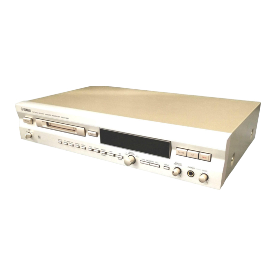
MINIDISC RECORDER
MDX-596
IMPORTANT NOTICE
Failure to follow appropriate service and safety procedures when servicing this product may result in personal
injury, destruction of expensive components and failure of the product to perform as specified. For these reasons,
we advise all YAMAHA product owners that all service required should be performed by an authorized
YAMAHA Retailer or the appointed service representative.
The presentation or sale of this manual to any individual or firm does not constitute authorization, certification or
recognition of any applicable technical capabilities, or establish a principle-agent relationship of any form.
Static discharges can destroy expensive components. Discharge any static electricity your body may have accumu-
lated by grounding yourself to the ground buss in the unit (heavy gauge black wires connect to this buss).
Turn the unit OFF during disassembly and parts replacement. Recheck all work before you apply power to the unit.
SERVICE MANUAL
IC DATA . . . . . . . . . . . . . . . . . . . . . . . . . . . . . . . 25-34
BLOCK DIAGRAM . . . . . . . . . . . . . . . . . . . . . . . 35-37
TEST POINT WAVEFORMS . . . . . . . . . . . . . . . 38-39
PRINTED CIRCUIT BOARD . . . . . . . . . . . . . . . 40-46
MD VOLTAGES . . . . . . . . . . . . . . . . . . . . . . . . . . . . . 47
SCHEMATIC DIAGRAM . . . . . . . . . . . . . . . . . . 48-50
REMOTE CONTROL TRANSMITTER . . . . . . . . . . . 51
PARTS LIST . . . . . . . . . . . . . . . . . . . . . . . . . . . . 52-61
GREASE APPLICATION DIAGRAM . . . . . . . . . . . . 62
MDX-596
Advertisement
Table of Contents
Troubleshooting

Related Manuals for Yamaha MDX-596


Summary of Contents for Yamaha MDX-596
-
Page 1: Table Of Contents
D E F G H I J K L M N O It has been assumed that basic service procedures inherant to the industry, and more specifically YAMAHA Products, are already P Q R S T U V W X known and understood by the users, and have therefore not been restated. -
Page 2: To Service Personnel
MDX-596 TO SERVICE PERSONNEL Critical Components Information AC LEAKAGE Components having special characteristics are marked Z EQUIPMENT WALL TESTER OR and must be replaced with parts having specifications equal OUTLET UNDER TEST EQUIVALENT to those originally installed. INSULATING TABLE WARNING: Laser Safety This product contains a laser beam component. -
Page 3: Rear Panels
MDX-596 Laser Diode Properties Magnetic head Material : GaAlAs Wavelength : 785 nm Emission duration : Continuous Pulse Durations and Max. Output at the lens of the Laser Pick Up Unit ; Read mode : 0.8 mW (Continuous) Write mode : Max 10 mW for 0.5s, Min. -
Page 4: Specifications
MDX-596 SPECIFICATIONS Digital audio system GENERAL System Power Supplies MiniDisc digital audio system A model AC 240 V, 50 Hz Disc G, B models AC 230 V, 50 Hz MiniDisc R models AC 110/120/220/240 V, 50/60 Hz Recording method Power Consumption... -
Page 5: Internal View
MDX-596 INTERNAL VIEW POWER TRANSFORMER MAIN (1) P.C.B. POWER SWITCH MD RECORDER UNIT MAIN (2) P.C.B. CB401 DISASSEMBLY PROCEDURES Top Cover (Remove parts in disassembly order as numbered.) 1. Removal of Top Cover a. Remove 4 screws ( q ) and 3 screw ( w ) in Fig. 1. - Page 6 MDX-596 Disassembly of MD Recorder Unit Remove the MD Recorder unit according to Steps 1 and 3 of the disassembly procedure (page 4). (K1)x1 Removal of MD Main P.C.B. and MD Mechanism (Fig. 3) ø2x 3mm 1. Remove 3 screws (K1) and then remove the Top Cover.
- Page 7 MDX-596 Removal of MD Loading P.C.B./Loading Motor (Fig. 5) (B1)x1 1. Remove 1 screw (B1). ø1.7x 6mm 2. Remove 3 hooks (B2) and then remove the MD Loading Motor Loading P.C.B. 3. Remove 2 screws (B3) and then remove the Loading MD Loading P.C.B.
-
Page 8: Adjustment & Test Mode
MDX-596 ADJUSTMENT & TEST MODE Servicing Procedure Perform adjustment and setup in the TEST mode. Specific adjustments and procedures vary depend- ing on the type of servicing performed. Required item TEMP standard EEPROM setting AUTO preliminary AUTO AUTO AFB EEPROM adjustment... - Page 9 MDX-596 2. How to set to each mode Every time the DISPLAY (forward) or EDIT (reverse) button is pressed, the mode changes. (For operation of each mode, refer to the section describing each mode.) AUTO_AJST (AUTO adjustment) AUT_AFB (AUTO AFB adjustment)
- Page 10 MDX-596 Description of TEST modes 1. EJECT mode To TEMP setting (of EEPROM setting) [ _ _ EJECT _ _ _ ] To CONTROL setting (of EEPROM setting) Laser power setting (record/reproduction power) is performed. 2. AUTO preliminary adjustment mode Automatic preliminary adjustment is performed.
- Page 11 MDX-596 Check item Check procedure Mode Judgement Possible cause and check content (Pin 3 of IC1401) OK (Move on to check w.) Playback power output “ppw” DC 0.2V – DC 1.5V Perform *1. Recording power output “rpw” DC 1.8V OK (End of checking.) –...
- Page 12 MDX-596 2. AUTO preliminary adjustment mode Disc in use: MMD-318 [for pre-adjustment] Step Setting method Remark Display Set the Test mode. No disc is loaded. [ EJECT ] [ LOADING ] Load a disc. [ AUTO _ AJST _ ] Auto adjustment menu Press the EDIT button once.
- Page 13 MDX-596 5. EEPROM setting mode Disc in use: Commercially available mini disc for recording (used to confirm/adjust setting values) Refer to p.15 for EEPROM setting. 6. TEST-PLAY mode Using the disc: Commercially available mini disc for recording (Use this mode to check that the playback function is provided at the specified address.)
- Page 14 MDX-596 Lead-in switch position adjustment Adjust the lead-in switch position so that it is between FF85 and FFD2. 1. Load a TDYS1 (SONY) (P/No. TX945850) disc for reproduction. 2. Loosen the screw (A1) (1 pc) attaching the mechanical switch P.C.B.
- Page 15 MDX-596 MECHANISM ADJUSTMENT When making an adjustment, be sure to connect an extension cable for servicing and an expansion P.C.B. as shown in Fig.12. 1. Optical pickup rating inspection method (Externally attached) Oscilloscope GND (TP1202) IC1201 No.4 pin 100K EIN (TP1253) IC1201 No.11 pin...
- Page 16 5. EEPROM setting mode Disc in use: Commercially available mini disc for recording (used to confirm/adjust setting values) 1) Start the TEST mode. 2) Load the disc. [AUTO AJST] 3) Press the DISPLAY button 6 times. [EEPROM SET] 4) Execute the procedure to have “EEPROM setting mode transition diagram” displayed and adjust the jog dial so that the same setting values as those in “EEPROM contents list”...
- Page 17 EEPROM CONTENTS LIST Focus setting (Focus) Slide setting (Sled) Item on display Set value Item on display Set value SLDLIM SLDLEV FZHLEV SLKLVk FOKLEVh SLKLVt FOKLEVL SLKLVm FOSTn SLBKm DISCJG SLKrio SLKroi SLK1io Spin setting (Spindle) SLK1oi Item on display Set value SPG-in Control setting (Control)
-
Page 18: Special Test Mode
MDX-596 SPECIAL TEST MODE How to set to the special test mode Press the POWER button while pressing the SET/ENTER button and the STOP button. Then all the indicators will light up. Operation procedure Every time the SET/ENTER button is pressed, lighting of indicators and items on the display change as follows. -
Page 19: Error Display
MDX-596 ERROR DISPLAY Error on display Description Countermeasure Can't REC • Check that the disc is free from any scratch, • DEFECT occurred 10 times continuously during REC- PLAY. dust, finger print, black spot, etc. and that • Recordable cluster became “0” due to occurrence of decentering, face deflection, etc. -
Page 20: Troubleshooting
MDX-596 Error on display Description Countermeasure Can' t Edit • Editing conditions were not satisfied with respect to • Wrong operation procedure was used. Try each editing function. again by using the correct procedure. • Check according to troubleshooting. TMP Over!! •... -
Page 21: Troubleshooting
MDX-596 TROUBLESHOOTING When MD fails to operate When the objective lens of the optical pickup becomes dirty, MD may fail to operate. Clean the objective lens first and check MD for reproduction function. If it still fails to operate, check according to the following flow charts. - Page 22 MDX-596 Disc cannot be loaded properly. Does the loading function work properly when a disc is inserted? Does No.5 pin of CN1401 become “H”? Check CN1401, CN1931 and SW1932. Does a change occur at either No.19 or 20 pin of IC1601? Check IC1401.
- Page 23 MDX-596 Normal reproduction Applicable when the E2-PROM value has been confirmed as normal in the test mode Is initialization done properly for reproduction of a high reflecting disc? Does the play time display count up properly? Check IC1201. Is the disc turning properly?
- Page 24 MDX-596 Recording/reproduction function Load a low reflection disc and after confirming the audio output in the normal reproduction mode, execute recording/reproduction. Does the recording function fail from the starting address? Check that the disc is not in the recording inhibited status.
- Page 25 MDX-596 Checking by using the test mode Spindle motor does not run. Check No.24 and 25 pins of IC1201 as well as solder Is a correct waveform provided at No.24 and 25 pins of IC1201 connections and parts of the peripheral circuit.
-
Page 26: Ic Data
MDX-596 IC DATA IC1101 : IR3R58M RF Signal Processing ADAGI EFM AGC ADAGC DIFF ADIPNF ADIP AGC REFI ADIPO BIAS REFO GND2 AOUT VCC2 OPICPW MODE DISC SGAIN BOUT DTEMP No. Pin Name Function RF signal input terminal 1 to input RF signal output from pickup... - Page 27 MDX-596 IC1101 : IR3R58M RF Signal Processing No. Pin Name Function ADIPNF AGC amplifier output terminal for ADIP signal ADAGC AGC smooth capacitor connecting terminal for ADIP signal ADAGI AGC amplifier input terminal for ADIP signal RF1, RF2 differential signal...
- Page 28 MDX-596 IC1201 : LR37814 ATRAC Encoder/Decoder Pin Name Function Focus error signal B Tracking error signal E Tracking error signal F VBAT Power supply voltage detect signal for constant voltage servo VDD1 Power supply terminal for digital section DGND Digital ground terminal...
- Page 29 MDX-596 IC1201 : LR37814 ATRAC Encoder/Decoder Pin Name Function Oscillation circuit output. 33.8688MHz Digital input signal DOUT Digital output signal PLLBVG External capacitor terminal for internal PLL DGND Ground terminal for digital section LRCK Output terminal for switching music data to Lch, Rch...
- Page 30 MDX-596 IC1202 : IX2474AF 4M Bit D-RAM Write Clock Clock Generator Generator Data Input CBR Refresh SELF Refresh Buffer Counter Timer MN42V4400 only DQ0~DQ3 Row Address Memory Row Decoder Word Driver Buffer Cell Row Address Column Decoder Sense Amp. Buffer...
- Page 31 MDX-596 IC1401 : iX0324AW MD System Microprocessor Pin Name Function 4M/16M 4M/16M DRAM select input 64M DRAM select input LDVAR LDVAR (Laser power adjustment output) ADJS ADJS (for automatic adjustment step check) CIN (Track count signal input) Unused UNLOCK ERR input (to unlock monitor PLL)
- Page 32 MDX-596 IC1401 : iX0324AW MD System Microprocessor Pin Name Function Input/output port P37 Input/output port P36 Input/output port P35 Input/output port P34 Input/output port P33 Input/output port P32 Input/output port P31 +3.15V INNSW Pick innermost track detect input L3 DATA...
- Page 33 MDX-596 IC1701 : UDA1347T AD Converter/DA Convereter V ref(A) V DDA(ADC) V SSA(ADC) V ADCP V ADCN 0dB/6dB VINL VINR switch V DDD DECIMATION FILTER UDA1347 V SSD DC-CANCELLATION FILTER DATAO DIGITAL L3-BUS INTERFACE INTERFACE DATAI SYSCLK DSP FEATURES INTERPOLATION FILTER...
- Page 34 MDX-596 IC6 : M30622M8-xxxFP IC6 : M30622M8-xxxFP Main System Microprocessor Main System Microprocessor /CS0 /CS1 /CS2 /CS3 /WRL/WR /WRH/BHE /BCLK /HLDA /HOLD /ALE /RDY/CLK /CTS /RTS /CLK /RXD /TXD /CTS /RTS /CTS /CLKS /CLK /RXD /TXD Port Name Function Unused (Pull-down at 10 kΩ) P96/ANEX1 Unused (Pull-down at 10 kΩ)
- Page 35 MDX-596 IC6 : M30622M8-xxxFP Main System Microprocessor Port Name Function P56/ALE Unused (Pull-down at 10 kΩ) P55//HOLD FLASH_GND P54//HLDA POWERDOWN Used at MD unit power failure P53/BCLK Unused (Pull-down at 10 kΩ) P52//RD Unused (Pull-down at 10 kΩ) P51//WRH,/BHE Unused (Pull-down at 10 kΩ)
-
Page 36: Block Diagram
MDX-596 BLOCK DIAGRAM (MD) 9 10 11 12 13 14 15 16 17 18 19 20 21 22 23 24 25 26 27 28 70 34 25 12 20 33 21 32 31 See page E-48/J-46 Schematic diagram MD unit... - Page 37 MDX-596 BLOCK DIAGRAM See page E-49/J-47 R.OUT L.OUT R.IN BUFFER BUFFER L.IN LEVEL AVCC Va+6V VR202 /LOADIN (MDM-07A) DSTB MDDATA KDATA ANALOG DECK MD-ST RESET PDOWN BACKUP DIGIN D1,2 DIGOUT PHONES PHONES LEVEL VR201 DIGITAL OPTICAL PHONES IC201 MUTE CONTROL...
-
Page 38: Test Point Waveforms
MDX-596 TEST POINT WAVEFORM POWER ON TOC READ(Low reflection disc) PLAY(Low reflection disc) 20ms/div 1ms/div 500ms/div 500ms/div CH1: 2V (DC, 10:1), CH2: 2V (DC, 10:1), CH3: 5V (DC, 10:1), CH4: 5V (DC, 10:1) CH1: 50V (DC, 10:1), CH2: 5V (DC, 10:1), CH3: 2V (DC, 10:1), CH4: 5V (DC, 10:1) -
Page 39: Printed Circuit Board
MDX-596 PRINTED CIRCUIT BOARD TO MAIN PWB : TEST POINT WAVEFORMS (See page E38/J36) TO MAGNET HEAD CW1501 CW1903 C1606 C1707 IC1702 TP1702 R1704 C1509 Q1702 CN1501 TP1520 TP1524 R1516 TP1301 C1304 R1513 R1515 TP1518 R1705 R1511 TP1517 R1703 TP1300... - Page 40 MDX-596 PRINTED CIRCUIT BOARD (Foil side) DIGITAL(OPTICAL) ANALOG MAIN (1) P.C.B. MAIN (2) P.C.B. LOUT L202 V+VB ROUT V-VB LEVEL PHONES ANALOG REC LEVEL DIGout GNDd DIGin PDOWN /MD-RES MD-ST DSCK SEARCH KDATA MDDATA DSTB J only GNDd GNDd GNDd GNDd D6.5/5V...
- Page 41 MDX-596 PRINTED CIRCUIT BOARD (Foil side) MAIN (3) P.C.B. MAIN (7) P.C.B. MAIN (4) P.C.B. FROM : POWER CORD POWER TO : MAIN (7) R only VOLTAGE SELECTOR TO : MAIN (3) #401 W302 TO : MAIN(4) W301 TO : MAIN(1) FROM: MAIN (1) MAIN (6) P.C.B.
-
Page 42: Md Voltages
MDX-595 PRINTED CIRCUIT BOARD MD VOLTAGES IC1101 IC1201 IC1401 MD MECHANISM PIN VOLTAGE PIN VOLTAGE NO. VOLTAGE VOLTAGE VOLTAGE SWITCH PWB-E1 MD LOADING 0.7V 1.3V 1.6V 0.7V 2.6V PWB-E2 0.7V 1.3V 0.7V 0.4V 0.2V 1.3V 2.6V 3.2V M902 1.3V 1.3V MD SLED MOTOR 1.3V 1.3V... - Page 43 NDX-596 SCHEMATIC DIAGRAM : TEST POINT WAVEFORMS (See page E38/J36) MD MAIN PWB-C C1204 C1232 0.001 0.047 C1113 C1116 C1117 C1205 TP1131 TP1202 R1119 TP1116 220K 1234 VCC1 EFMAGC TP1201 TP1212 C1123 DADATA C1201 AVCC1 DADATA EFMO-I ADAGI EFMO-I ADDATA EFMI ADDATA C1121...
-
Page 44: Schematic Diagram
MDX-596 IC3 ~ 5 : NJM2068D-D IC201 : BA15218N SCHEMATIC DIAGRAM Dual OP-Amp Dual OP-Amp –IN MUTING – – – – –IN –V -5.9 -5.9 IC1 : TC74HCT04AP Hex Inverters -5.9 -5.9 P-E48/J46 -6.0 [K-7] IC2 : TC74VHC157F BUFFER BUFFER... - Page 45 NDX-596 SCHEMATIC DIAGRAM IC601 : LC75710NE FL Driver -26.7 -26.7 -26.7 AM32 AM31 -26.7 AM30 -26.7 AM29 FL DRIVER AM28 -26.7 AM27 -26.7 AM26 TEST AM25 -26.7 AM24 -26.7 OSCO AM23 OSCI AM22 AM21 AM20 P-E49/J47 AM19 AM18 [C-8] AM17 SHIFT DC RAM REGISTER...
-
Page 46: Remote Control Transmitter
MDX-596 REMOTE CONTROL TRANSMITTER SCHEMATIC DIAGRAM KI/O8 KI/O5 IED1 KI/O7 KI/O4 KI/O3 SI/LED KI/O2 KI/O1 KI/O0 XOUT 455KHz RESET 3(V) 2.2Ω 47µF 220pF 220pF CUSTOM DATA CUSTOM DATA FUNCTION FUNCTION (HEX) (HEX) (HEX) (HEX) A–B DISPLAY DISPLAY SCROLL SCROLL A - B REPEAT &... -
Page 47: Parts List
MDX-596 WARNING PARTS LIST Components having special characteristics are marked Z and must be replaced with parts having specifications equal to those originally installed. Carbon resistors (1/6W or 1/4W) are not included in the ELECTRICAL PARTS ELECTRICAL PARTS List. For the parts No. of the carbon resistors, refer to last page. - Page 48 MDX-596 P.C.B. MAIN Schm Schm Ref. PART NO. Description Ref. PART NO. Description V5731000 P.C.B. MAIN(R) UR837100 C.EL 10uF V5731100 P.C.B. MAIN(A) UA952220 C.MYLAR 220pF V5731200 P.C.B. MAIN(BG) UR866100 C.EL V3733000 CN UR846470 C.EL 4.7uF VT707200 L.EMIT TOTX178 UA952560 C.MYLAR 560pF VT620100 L.DTCT...
- Page 49 MDX-596 P.C.B. MAIN Schm Schm Ref. PART NO. Description Ref. PART NO. Description * D5 VG437600 DIODE.ZENR MTZJ5.6A 5.6V iD040040 2SD400 * D6 VG436500 DIODE.ZENR MTZJ3.9A 3.9V VS883300 TR 2SB1565 E,F VU264100 DIODE 1SR139-400 VC141900 TR 2SB941 P,Q VU264100 DIODE...
- Page 50 MDX-596 P.C.B. MD MAIN Schm Schm Ref. PART NO. Description Remarks Ref. PART NO. Description Remarks P.C.B. MD MAIN C1506 AAX02540 C.CHP 100pF VCCCCY1HH101J C1100 AAX02530 C.CHP 4.7uF RCKZ0003AWZZ C1507 AAX02660 C.CHP 0.047uF 16V VCKYCY1CB473K C1107 AAX02650 C.CHP 0.033uF 16V...
- Page 51 MDX-596 P.C.B. MD MAIN Schm Schm Ref. PART NO. Description Remarks Ref. PART NO. Description Remarks * IC1201 AAX17310 LR37814 VHILR37814/1 * R1123 AAX17680 R.CAR.CHP 12KΩ 1/16W VRSCY1JB123J IC1202 AAX02150 IX2474AF RHIX2474AFZZ * R1124 AAX17710 R.CAR.CHP 2.2KΩ 1/16W VRSCY1JB222J * IC1300...
- Page 52 MDX-596 P.C.B. MD MAIN CHIP RESISTORS Schm Schm Ref. PART NO. Description Remarks Ref. PART NO. Description Remarks R1463 AAX01760 R.CAR.CHP 10KΩ 1/16W VRSCY1JB103J * R1803 AAX17750 R.CAR.CHP 33KΩ 1/16W VRSCY1JB333F R1510 AAX01750 R.CAR.CHP 1KΩ 1/16W VRSCY1JB102J R1804 AAX02000 R.CAR.CHP 390Ω...
-
Page 53: Exploded View
MDX-596 EXPLODED VIEW R model only R model only 1-32 1-21 1-32 1-32 1-16 1-17 1-13 1-11 1-32 1-27 1-32 1-26 1-24 1-12 1-32 1-15 200-1 1-32 1-22 1-31 1-23... - Page 54 MDX-596 MECHANICAL PARTS Ref. PART NO. Description Remarks Markets MF119200 FLEXIBLE FLAT CABLE 19P 200mm * 1-11 V5235500 FRONT PANEL * 1-11 V5235600 FRONT PANEL * 1-12 V3080600 PANEL, SUB * 1-12 V3080700 PANEL, SUB 1-13 V3082300 SPRING 1-15 V3081800 SUPPORT, VR...
- Page 55 MDX-596 EXPLODED VIEW (MD Recorder Unit) 33x2 512x2 33x2 M903 SW1934 SW1932 SW1933 PWB-C PWB-E2 SW1931 SW1930 510x2 506x2 M902 SW1936 PWB-E1 501x2 M901 505x3...
- Page 56 MDX-596 MECHANICAL PARTS (MD Recorder Unit) Ref. PART NO. Description Remarks Markets V5063300 MD RECORDER UNIT V5063300 AAX16830 LD BASE LCHSM0089AWZZ AAX16840 MD BASE LCHSM0090AWZZ AAX16860 CARTRIDGE HOLDER ASSY LHLDX3007AWM1 AAX16980 SLIDER LEVER ASSY MLEVF0051AWM1 AAX17100 HOLDER ARM MLEVF0046AWFW AAX16960 SWITCH PLATE...
-
Page 57: Grease Application Diagram
MDX-596 GREASE APPLICATION DIAGRAM M902 Grease : Molykote PG-662 : HYDRO-FLUTE EP-68... - Page 58 MDX-596 Parts List for Carbon Resistors Value 1/4W Type Part No. 1/6W Type Part No. Value 1/4W Type Part No. 1/6W Type Part No. 1.0 Ω 3100 3100 7100 10 kΩ 7100 HJ35 HF85 HF45 HF45 1.8 Ω 3180 7110 11 kΩ...
- Page 59 MDX-596...