Table of Contents
Advertisement
Quick Links
SERVICE MANUAL
Product Type: DVD+VCR
Chassis: D35 (DECK), DP-7C(MD)
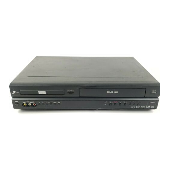
Manual Series: XBV323
Manual Part #: 3829RVN006P
Model Line: F
Product Year: 2003
CONTENTS
....................................................
Summary
Cabinet & Main Chassis
....................................................
Electrical
Mechanism of VCR Part
Mechanism of DVD Part
....................................................
Parts List
Published September 2003
by Technical Publications
Zenith Electronics Corporation
201 James Record Road
Huntsville, Alabama 35824-1513
Copyright © 2003 by Zenith Electronics Corporation
1
.............................
2
3
.............................
4
.............................
5
6
Model Series:
XBV323
Advertisement
Chapters
Table of Contents
Troubleshooting

Related Manuals for Zenith XBV323 Series


Summary of Contents for Zenith XBV323 Series
- Page 1 Cabinet & Main Chassis ............ Electrical ......Mechanism of VCR Part ......Mechanism of DVD Part ............ Parts List Published September 2003 by Technical Publications Zenith Electronics Corporation 201 James Record Road Huntsville, Alabama 35824-1513 Copyright © 2003 by Zenith Electronics Corporation...
- Page 3 SECTION 1 SUMMARY CONTENTS PRODUCT SAFETY SERVICING GUIDELINES FOR VIDEO PRODUCTS ..... 1-2 SERVICING PRECAUTIONS ....................1-3 SPECIFICATIONS ........................1-4...
-
Page 4: Product Safety Servicing Guidelines For Video Products
When servicing this product, under no circumstances should the original design be modified or altered without permission from Zenith Electronics Corporation. All components should be replaced only with types identical to those in the original circuit and their physical location, wiring and lead dress must conform to original layout upon completion of repairs. -
Page 5: Servicing Precautions
SERVICING PRECAUTIONS CAUTION: Before servicing the DVD+VCR covered by this Electrostatically Sensitive (ES) Devices service data and its supplements and addends, read and fol- Some semiconductor (solid state) devices can be damaged low the SAFETY PRECAUTIONS. NOTE: if unforeseen cir- easily by static electricity. -
Page 6: Specifications
SPECIFICATIONS General Power requirements AC 120V ,60 Hz Power consumption Dimensions (approx.) 430 X 97.5 X 293 mm (16.9 x 3.9 x 11.5 inches)(w x h x d) Mass (approx.) 4.8 kg (10.58 lbs) Operating temperature 5 °C to 40 °C (41 °F to 104 °F) Operating humidity 5 % to 90 % Signal system... - Page 7 SECTION 2 CABINET & MAIN CHASSIS CONTENTS 1. EXPLODED VIEWS ........................2-2 1. Cabinet and Main Frame Section ...................2-2 2. Packing Accessory Section ....................2-3...
-
Page 8: Cabinet And Main Frame Section
EXPLODED VIEWS 1. Cabinet and Main Frame Section... -
Page 9: Packing Accessory Section
2. Packing Accessory Section OPTIONAL PARTS 810 CABLE ASS'Y RF CABLE(COAXIAL) PLUG ASS'Y 1WAY BATTERY PLUG ASS'Y 2WAY REMOCON INSTRUCTION ASSEMBLY PACKING PACKING BOX CARTON... -
Page 10: Table Of Contents
SECTION 3 ELECTRICAL CONTENTS OVERALL WIRING DIAGRAM 5. LENS CONTROL RELATED SIGNAL ......3-2 (NO DISC CONDITION) ........3-67 VCR PART 6. LASER POWER CONTROL RELATED SIGNAL(NO DISC CONDITION)......3-68 ELECTRICAL ADJUSTMENT 7. DISC TYPE JUDGEMENT WAVEFORMS....3-68 PROCEDURES ............3-3 8. FOCUS ON WAVEFORMS ........3-70 VCR ELECTRICAL TROUBLESHOOTING 9. -
Page 11: Overall Wiring Diagram
OVERALL WIRING DIAGRAM K-RTN K-RTN 5.3VA PM602 PM603 A_MUTE_R A_MUTE_L D_A_R_OUT D_A_L_OUT C_V_OUT(DVD) Pb/C PDV03 PMD02 DATA DATA RESET K.RTN OPTICAL COAXIAL S/COMPO PVD02 PMD01 12VA(DRUM) 5.0V 5.3VA PMP01 ERASE FULL P3D03 A.PB A.REC A/E(-) A/E(+) CTL(-) CTL(+) P3D02 DRUM DFG/FG 12VA(DRUM) MOTOR... -
Page 12: Vcr Part
VCR PART ELECTRICAL ADJUSTMENT PROCEDURES 1. Servo Adjustment 1) PG Adjustment • Test Equipment a) OSCILLOSCOPE b) NTSC MODEL : NTSC SP TEST TAPE • Adjustment And Specification MODE MEASUREMENT POINT ADJUSTMENT POINT SPECIFICATION V.Out PLAY R/C TRK JIG KEY 6.5 ±... -
Page 13: Vcr Electrical Troubleshooting Guide
VCR ELECTRICAL TROUBLESHOOTING GUIDE 1. Power(SMPS) CIRCUIT (1) No 5.3VA (SYS/Hi-Fi/TUNER) (2) No 12VA (TO CAP, DRUM MOTOR) NO 5.3VA. NO 12VA. Replace F101. Is the Vcc(13V) supplied Check or Replace Is F101 normal? (Use the same type) to (+) terminal in D115? D110. - Page 14 VCR ELECTRICAL TROUBLESHOOTING GUIDE (4) No 5V (TO DVD) (5) No 33V (TUNER) NO 5V. No 33V. Is 5.3VA put into Check the Power 5.3VA Line Check. Is Q162 Base “H”? Q160 Emitter? Control. Check the Power Check or Replace Is Q162 Base “H”? Control.
- Page 15 VCR ELECTRICAL TROUBLESHOOTING GUIDE (8) No 8V(TO DVD) (9) No 3.3V(TO DVD) NO 8V. NO 3.3V. Check or Replace Check or Replace Is Vcc(13V) supplied to Is Vcc(4V) supplied (+) terminal in D114? to IC152 Pin1? D110. D111. Check or Replace Check the Power Is Vcc(12V) supplied Is the Q162 Base...
-
Page 16: System/Key Circuit
VCR ELECTRICAL TROUBLESHOOTING GUIDE 2. SYSTEM/KEY CIRCUIT (1) AUTO STOP Auto Stop Check the Drum Motor Does the SW30 waveform appear at IC501 Pin18? signal. Do T/UP Reel Pulses Do the T-UP Reel Pulses Does 5V appear at the appear at the point appear at IC501 Pin80? RS501? between R556 and R536? -
Page 17: Servo Circuit
VCR ELECTRICAL TROUBLESHOOTING GUIDE 3. SERVO CIRCUIT (1) Unstable Video in PB MODE Does the Noise level of the screen change periodically? Do the CTL pulses appear Is the height adjustment of at IC501 Pin97? the CTL Head accurate? Readjust the height of the Confirm the CFG CTL Head. - Page 18 VCR ELECTRICAL TROUBLESHOOTING GUIDE 2. SERVO CIRCUIT (3) When the Capstan Motor doesn’t run, When the Capstan Motor doesn’t run, Refer to “SMPS(CAPSTAN/12Volt) Does 12VA appear at PMC01? Trouble Shooting”. Does 2.8V appear at PMC01? Check the PMC01 and the Capstan Does the PWM signal appear at IC501 Pin77? Motor Ass’y.
-
Page 19: Osd Circuit
VCR ELECTRICAL TROUBLESHOOTING GUIDE 2. SERVO CIRCUIT (4) Keys do not work Keys do not work Is 5V applied to IC501 Refer to “SMPS 5.3VA Pin79? Trouble Shooting”. Does LED or FLD change Replace the defective when a function button is switches. -
Page 20: Y/C Circuit
VCR ELECTRICAL TROUBLESHOOTING GUIDE 5. Y/C CIRCUIT (1) No Video in EE Mode, No Video in EE Mode Does the Video signal Does the Video signal Check DVD Video Input appear at IC301 appear at IC302 (IC802, Pin29), Tuner Pins28, 30, 32? Pins1, 5? Video Input (TU701 Pin24), Line Video Input (JK801),... - Page 21 VCR ELECTRICAL TROUBLESHOOTING GUIDE 3. Y/C CIRCUIT (2) When the Y(Luminance) signal doesn’t appear on the screen in PB Mode, Is 5V applied to IC301 Check the line of the REG 5V Line. (Power Circuit) Pins23, 44, 45, 52, 68, 77? Is the Y/C Bus siganl Refer to ‘SYSTEM Y/C applied to IC301 Pins53,...
- Page 22 VCR ELECTRICAL TROUBLESHOOTING GUIDE 3. Y/C CIRCUIT (3) When the C(Color) signal doesn’t appear on the screen in PB Mode, Is 5V applied to IC301 Check the line of the REG 5V Line. (Power Circuit) Pins23, 44, 45, 52, 68, 77? Does the Color signal Is X301 (3.58MHz) appear at IC301...
- Page 23 VCR ELECTRICAL TROUBLESHOOTING GUIDE 3. Y/C CIRCUIT (4) When the Video signal doesn’t appear on the screen in REC Mode, REC mode Is EE mode normal? Check the EE mode Is brightness normal? Is color normal? Is the brightness signal sup- Does signal appear at Check X301 oscillation IC301 Pins41, 50?
-
Page 24: Hi-Fi Circuit
VCR ELECTRICAL TROUBLESHOOTING GUIDE 6. Hi-Fi CIRCUIT (1) No Sound(EE Mode) No Sound. Check the SIF.IN of IC801 Pins57. Check the TU701 SIF Pin13. Check the DVD Audio of IC801 Check the DVD MODULE. (PMD02 Pins9, 11). Pins12, 74. Check the AV1 Audio of IC801 Check the Rear Jack. - Page 25 VCR ELECTRICAL TROUBLESHOOTING GUIDE 3. Y/C CIRCUIT (2) Hi-Fi Playback No Sound. Check the Vcc of IC801 Check Power. (Pins3, 5, 15, 32, 36, 46, 54). Check the Hi-Fi Selection switch. Check IC501 Pin19 (A.H/SW) (IC801 Pin39) and the Tape quality. Is the RF Envelope at IC801 Pin23 over 3Vp-p? Check IC801 Pin37(Data),...
- Page 26 VCR ELECTRICAL TROUBLESHOOTING GUIDE (3) Hi-Fi REC No recorded Hi-Fi Audio Signal Check Vcc of IC801. Check Power. (Pins3, 5, 15, 32, 36, 46, 54) Check ports of µ-CPM. Check IC801 Pin37(Data), Pin38(CLOCK). (IC501 Pins71, 72) Check Audio input signal of IC801 Do Audio signals appear at IC801 Pin6? Pin57(TU.A.), 7, 69(DVD.A.), 11, 73(AVI.A.), 9, 71(AV2.A.)
-
Page 27: Tuner/If Circuit
VCR ELECTRICAL TROUBLESHOOTING GUIDE 7. Tuner/IF CIRCUIT (1) No Picture on the TV screen No picture on the TV screen Does the Video signal Is +33V applied to TU701 Check 33V line. appear at TU701 Pin16. Pin14? Is +5V applied to TU701 Check 5V line. - Page 28 VCR ELECTRICAL TROUBLESHOOTING GUIDE (2) No Sound No Sound. Check the Vcc of TU701 Pins3, 14. Check 5.2V, 33V Line. Check the Tuner SiF signal at IC801 Check the Tuner SIF of TU701 Pin13. Pin57. 1. Check the Vcc(5.3VA, 9V) of IC801 Check the Audio of IC801 Pins78, 80.
-
Page 29: Block Diagrams
BLOCK DIAGRAMS 1. POWER(SMPS) BLOCK DIAGRAM R101 SNUBBER TO SYS RECTIFIER & BD101 BLOCK FD(-) F102 SMOOTHING (D101, R104, (D107, C121, C105, C106) ZD101, R167, R168) TO SYS C103 FD(+) RECTIFIER & TO SYS SMOOTHING -27VA (D108, C130, R118) RECTIFIER & SMOOTHING TO CAP MOT 12VA... -
Page 30: Tu/If Block Diagram
2. TU/IF BLOCK DIAGRAM 875 MOD A.IN MOD CTL 106 5.0V VCR 'H' REG. BLOCK 671 MOD V.IN IIC CLK REG. BLOCK IIC DATA 781 SIF OUT TU.V.OUT 3-22 3-23... -
Page 31: Y/C Block Diagram
3. Y/C BLOCK DIAGRAM (PB Mode) (REC Mode) 55 54 53 51 50 49 48 47 55 54 53 320FH SERIAL VX01 DECODER AUDIO C-ROT MUTE RF-SW HA SW CLAMP CLAMP EP REC EP PB 'A' CLAMP IC302 EP PB 'B' CLAMP TU/LINE1 MAIN... -
Page 32: Normal Audio Block Diagram
4. NORMAL AUDIO BLOCK DIAGRAM (EE Mode) (PB Mode) (REC Mode) 3-26 3-27... -
Page 33: Hi-Fi Block Diagram
5. Hi-Fi BLOCK DIAGRAM Hi-Fi/ AUDIO INPUT 26 27 BLOCK A.OUT 'L' DVD A.IN 'L' A.OUT To JACK A.OUT 'R' IC801 DVD A.IN 'R' AV1 A.IN 'L' LA72670M AV1 A.IN 'R' MODULATOR AV2 A.IN 'L' A.OUT (To Tu) AV2 A.IN 'R' NORMAL AUDIO OUT(To AVCP) NORMAL AUDIO... -
Page 34: System Block Diagram
6. SYSTEM BLOCK DIAGRAM TO/FROM DECK TO/FROM AVCP 5.3VA MODE S/W MS501 95 94 87 12 9 18 13 16 59 CV IN I-Limit COMP IN MODE S1 MODE S1 MODE S2 REC 'H' MODE S2 MODE S3 MODE S4 C.ROT MODE S3 A.MUTE'H'... -
Page 35: Circuit Diagrams
2. Voltages are DC-measured with a digital voltmeter MODIFIED OR ALTERED WITHOUT PERMISSION IMPLEMENTATION OF THE LATEST SAFETY AND during Play mode. FROM THE ZENITH ELECTRONICS CORPORATION. PERFORMANCE IMPROVEMENT CHANGES INTO ALL COMPONENTS SHOULD BE REPLACED ONLY THE SET IS NOT DELAYED UNTIL THE NEW SERVICE WITH TYPES IDENTICAL TO THOSE IN THE ORIGI- LITERATURE IS PRINTED. -
Page 36: Tu/If Circuit Diagram
2. TU/IF CIRCUIT DIAGRAM 3-34 3-35... -
Page 37: Pb/C
3. A/V CIRCUIT DIAGRAM IC301 doesn’t operate. IC301 Pins 53, 54, 55 are defective. PB COLOR Signal does not appear. IC301 is defective. PB COLOR Signal does not appear. IC301 Pin 57 is defective. Auto Tracking has failed. IC301 Pin 59 is defective. EE, PB Screen doesn’t appear. -
Page 38: Hi-Fi Circuit Diagram
4. Hi-Fi CIRCUIT DIAGRAM No Audio IC801 Pins37, 38 aredefective. KTC3875 No Hi Fi Audio 23 Pin is defective. '02. 12. 04 R13734C 3-38 3-39... -
Page 39: Jack Circuit Diagram
5. JACK CIRCUIT DIAGRAM ONLY SVHS OPTION ONLY COMPONENT OPTION 3-40 3-41... -
Page 40: System Circuit Diagram
6. SYSTEM CIRCUIT DIAGRAM • Reset is defective. • Set dead. IC504 is defective. MTZ5.6B MTZ5.6B VCR LCD DVD LED IC501 M37762 µ-COM will not operate. X502 is defective. CLOCK SETTING will not operate. X501 is defective. C542 680P µ-COM is unstable. Q501, Q503 are defective. -
Page 41: Timer Circuit Diagram
7. TIMER CIRCUIT DIAGRAM 3-44 3-45... -
Page 42: Waveforms
• WAVEFORMS * IC301 Waveform * IC501 Waveform Stop : 10.0KS/s 280 Acqs Stop : 250KS/s 299 Acqs Stop : 10.0KS/s 18 Acqs Trigger Position: 12% Stop : 10.0KS/s 27 Acqs 1.00 V M 5.00ms 3.04 V 1.00 V M5.00ms 3.04 V 1.00 V M 200µs... -
Page 43: Circuit Voltage Chart
• CIRCUIT VOLTAGE CHART MODE MODE MODE MODE MODE MODE Base Emitter Collector Location PLAY PLAY PLAY PLAY PLAY PLAY PIN NO. PIN NO. PIN NO. PIN NO. PIN NO. PIN NO. I C 3 0 1 0.68 0.93 5.19 5.19 3.86 0.23... -
Page 44: Printed Circuit Diagrams
PRINTED CIRCUIT DIAGRAMS 1. VCR P.C.BOARD LOCATION GUIDE 3-50 3-51... -
Page 45: Key 1(Left) P.c.board
2. KEY 1(LEFT) P.C.BOARD LOCATION GUIDE 3. KEY 2(RIGHT) P.C.BOARD LOCATION GUIDE 3-52 3-53... -
Page 46: Power P.c.board
4. POWER P.C.BOARD NOTES) Warning NOTES) Parts that are shaded are critical NOTES) With respect to risk of fire or LOCATION GUIDE NOTES) electricial shock. 3-54 3-55... -
Page 47: Dvd Section
DVD SECTION ELECTRICAL TROUBLESHOOTING GUIDE 1. System operation flow Power On 1. 8032 initializes SERVO, DSP & RISC registers 2. Write RISC code to SDRAM 3. Reset RISC Show LOGO Tray Closed? Tray Close to Closed position SLED at Inner Side? SLED Moves to Inner Position 1. -
Page 48: Test & Debug Flow
2. Test & debug flow TEST Check the AC Vol tage Check the POWER PART Power PCBA (110V or 220V) Switch on the Power PCBA the DC Voltage outputs OK? Check the POWER PART (5V, 3.3V, 8V, 12V) Is 3.3V and 2.5V DC Check the regulators or diode(D601). - Page 49 RESET or Power On. Flash Check connection lines between FLASH Memory operates Show LOGO? & MT1379 and the FLASH access time properly? whether is sui table or not. SDRAM Check connection lines between SDRAM(IC502,IC503) & MT1379 and the works properl y? SDRAM is damaged.
- Page 50 Does the SLED move Check the connection line of Motor Driver STBY to inner side when it is at STBY signal . Pin is High? outer position? Check the related circuit of Motor Driver STBY FMSO. Pin is High? Check the amp circuit on SL+ and SL- output motor driver.
- Page 51 Check the laser power circuit Laser turns on when LD01 or LD02 output on MT1336 and connecting to reading disc? properly? power transistor. (Q204, Q205) Collector Check the related circuit on voltage of power laser power transi stor transistor is OK? ( Q204, Q205) Check cable connection between transistor output and pick-up head.
- Page 52 Proper Check connections between signals on A, B, C, Focus ON OK? MT1336 and pick-up head. D of MT1336 Check the related circuit Proper FEO signal on MT1336 FEO sugnal . on MT1336? Check FEO connection between MT1336 and MT1379 Check the related Proper FEO signal Track On OK?
- Page 53 Audio Normal DAC received Check connection between MT1379 Audio output & Audio DAC. (Check VRST#, ACLK, correct data stream? when disc playback? ABCK, ASDAT3) Normal Check the related circuit of Audio DAC Audio DAC. (Check Audio out? (IC401) out Pin 14, 15,18,19) Check Audio filter, amplify, mute circuit.
-
Page 54: Details And Waveforms On System Test And Debugging
DETAILS AND WAVEFORMS ON SYSTEM TEST AND DEBUGGING 1. SYSTEM 27MHz CLOCK,RESET,FLASH R/W SIGNAL 1) MT1379 main clock is at 27MHz(X501) 3.8V, 27MHz FIG 1-1 2) MT1379 & MT1336 reset is high active. Power Cord in 5.2VA PWR_CTL(CN505 PIN 7) M_RESET(CN505 PIN 9) URST(IC501 PIN 188) FIG 1-2... - Page 55 3) RS232 waveform during procedure(Downloading) TXD(J6 PIN3) RXD(J6 PIN 2) FIG 1-3 4) Flash R/W enable signal during download(Downloading) FRD(IC5A1 PIN 28) FWR(IC5A1 PIN 11) FIG 1-4 3-64...
-
Page 56: Sdram Clock
2. SDRAM CLOCK 1) MT1379 main clock is at 27MHz(X501) DCLK = 93MHz, Vp-p=2.2, Vmax=2.7V (IC502,IC503 PIN 35) FIG 2-1 3. TRAY OPEN/CLOSE SIGNAL 1) Tray open/close waveform OPEN((CN203 PIN 3) CLOSE(CN203 PIN 2) TROPEN(IC202 PIN 1) TRCLOSE(IC202 PIN 2) FIG 3-1 3-65... - Page 57 2) Tray close waveform OPEN((CN203 PIN 3) CLOSE(CN203 PIN 2) TROPEN(IC202 PIN 1) TRCLOSE(IC202 PIN 2) FIG 3-2 3) Tray open waveform OPEN((CN203 PIN 3) CLOSE(CN203 PIN 2) TROPEN(IC202 PIN 1) TRCLOSE(IC202 PIN 2) FIG 3-3 3-66...
-
Page 58: Sled Control Related Signal (No Disc Condition)
4. SLED CONTROL RELATED SIGNAL (NO DISC CONDITION) FMSO(2.0V/1.4V/1.0V) (IC501 PIN 19) STBY(5V) – (IC201 PIN 50) SL+(4.7V/3.6V/1.9V) (IC202 PIN 12) SL-(5.3V/3.7V/2.5V) (IC202 PIN 13) FIG 4-1 5. LENS CONTROL RELATED SIGNAL(NO DISC CONDITION) FOSO(1.5V/1.4V/1.3V) (IC501 PIN 12) F+(4.0V/3.6V/3.2V) (IC202 PIN 9) F-(4.0V/3.6V/3.2V) (IC202 PIN 8) FIG 5-1... -
Page 59: Laser Power Control Related Signal(No Disc Condition)
6. LASER POWER CONTROL RELATED SIGNAL(NO DISC CONDITION) MDI1(0V/180mV) (IC201 PIN 124) LD01(5.0V//3.5V) IC201 PIN 125) LD02(5.0V/3.6V) (IC201 PIN 126) FIG 6-1 7. DISC TYPE JUDGEMENT WAVEFORMS F+(IC202 PIN 9) FE(IC201 PIN 18) RFL(IC201 PIN 19) FIG 7-1 (DVD) 3-68... - Page 60 F+(IC202 PIN 9) FE(IC201 PIN 18) RFL(IC201 PIN 19) FIG 7-2 (DVD) F+(IC202 PIN 9) FE(IC201 PIN 18) RFL(IC201 PIN 19) FIG 7-3 (CD) 3-69...
-
Page 61: Focus On Waveforms
F+(IC202 PIN 9) FE(IC201 PIN 18) RFL(IC201 PIN 19) FIG 7-4 (CD) 8. FOCUS ON WAVEFORMS FE(IC201 PIN 18) FOSO(IC501 PIN12) F+(IC202 PIN 9) F-(IC202 PIN 8) FIG 8-1 (DVD) 3-70... -
Page 62: Spindle Control Waveforms (No Disc Condition)
FE(IC201 PIN 18) FOSO(IC501 PIN12) F+(IC202 PIN 9) F-(IC202 PIN 8) FIG 8-2 (CD) 9. SPINDLE CONTROL WAVEFORMS (NO DISC CONDITION) DMSO(1.4V/1.8V) (IC501 PIN 18) SP-(3.6V/2.4V) (IC202 PIN 10) SP+(3.6V/4.8V) (IC202 PIN 11) FIG 9-1 3-71... -
Page 63: Tracking Control Related Signal(System Checking)
10. TRACKING CONTROL RELATED SIGNAL(System checking) TE(IC201 PIN 21) TRSO(IC501 PIN 13) T-(IC202 PIN 7) T+(IC202 PIN 6) FIG 10-1(DVD) TE(IC201 PIN 21) TRSO(IC501 PIN 13) T-(IC202 PIN 7) T+(IC202 PIN 6) FIG 10-2(CD) 3-72... -
Page 64: Rf Waveform
11. RF WAVEFORM RFOP(2.3V/1.1V) (IC201 PIN 6) RFON(0.8V/2.0V) (IC201 PIN 7) FIG 11-1 12. MT1379 AUDIO OPTICAL AND COAXIAL OUTPUT (ASPDIF) (IC501 PIN 153) FIG 12-1 3-73... -
Page 65: Mt1379 Video Output Waveforms
13. MT1379 VIDEO OUTPUT WAVEFORMS 1) Full colorbar signal(CVBS) (IC604 PIN 23) FIG 13-1 2) Y (IC604 PIN 21) FIG 13-2 3-74... -
Page 66: Audio Output From Audio Dac
3) C (IC604 PIN 26) FIG 13-3 14. AUDIO OUTPUT FROM AUDIO DAC 1) Audio L/R (JK601 PIN 4,5) FIG 14-1 3-75... - Page 67 2) Audio related Signal ASDATA3 ASDAT3(IC501 PIN 157) ABCK(IC501 PIN 148) ALRCK(IC501 PIN 149) FIG 14-2 3-76...
-
Page 68: Block Diagrams
BLOCK DIAGRAMS 1. Overall Block Diagram MA11,BA1 DQM[2:3] MUTE DQ[16:31] ASPDIF Y[1:6] CVBS ASPECT DQM[0:1] DQ[00:15] URST F+,F-,T+,T- SP+,SP- SL+,SL- LOAD+,LOAD- DECK MECHANISM 3-77... -
Page 69: Servo Block Diagram
2. SERVO Block Diagram DQ[16:31] DQ[0:15] 3-78... -
Page 70: Mpeg & Memory Block Diagram
3. MPEG & MEMORY Block Diagram AD[0:7] A[0:19] DQ[16:31] PWR,PCE,PRD DQM2,DQM3 CS,DCKE,MA[0:10] DCLK,WE,CAS,RAS M_REQ VFD_TXD VFD_SCK DQ[0:15] DQM0,DQM1 VFD_RXD URST,S_REQ 3-79... -
Page 71: Video & Audio Block Diagram
4. VIDEO & AUDIO Block Diagram 3-80... -
Page 73: Circuit Diagrams
CIRCUIT DIAGRAMS 1. SYSTEM CIRCUIT DIAGRAM No Power on No Video signal. System not working or screen is abnormal Program download fail Digitron will not display Video signal Y System not working Video signal Color 3-81 3-82... -
Page 74: Rf & Dsp Servo Circuit Diagram
2. RF & DSP SERVO CIRCUIT DIAGRAM No CD/DVD LD 3-83 3-84... -
Page 75: Audio Circuit Diagram
3. AUDIO CIRCUIT DIAGRAM 3-85 3-86... -
Page 76: Av/Jack Circuit Diagram
4. AV/JACK CIRCUIT DIAGRAM 3-87 3-88... -
Page 77: Circuit Voltage Chart
• CIRCUIT VOLTAGE CHART IC201 IC202 IC501 IC502 IC505 IC510 IC5A1 IC401 IC402 IC5C1 IC201 IC202 IC501 IC502 IC505 IC510 IC5A1 IC401 IC402 IC5C1 (MT1336E) (MOTOR) (MT1379) (SDRAM) (EEPROM) (BUFFER) (FLASH) (CS4391) (AMP) (MM1623XFBE) (MT1336E) (MOTOR) (MT1379) (SDRAM) (EEPROM) (BUFFER) (FLASH) (CS4391) (AMP) - Page 78 Q201 Q202 Q203 Q204 IC201 IC202 IC501 IC502 IC505 IC510 IC5A1 IC401 IC402 IC5C1 (MT1336E) (MOTOR) (MT1379) (SDRAM) (EEPROM) (BUFFER) (FLASH) (CS4391) (AMP) (MM1623XFBE) STOP PLAY STOP PLAY STOP PLAY STOP PLAY PIN STOP PLAY STOP PLAY STOP PLAY STOP PLAY STOP PLAY STOP PLAY STOP PLAY STOP PLAY STOP PLAY STOP PLAY 5.14 4.34...
-
Page 79: Printed Circuit Diagrams
PRINTED CIRCUIT DIAGRAMS 1. MTR P.C.BOARD LOCATION GUIDE 3-93 3-94... - Page 81 SECTION 4 MECHANISM OF VCR PART CONTENTS 1. Mechanism Alignment Position Check .4-13 DECK MECHANISM PARTS 2. Preparation for Adjustment ..4-14 LOCATIONS 3. Checking Torque ....4-14 •...
-
Page 82: Deck Mechanism Parts Locations
DECK MECHANISM PARTS LOCATIONS • Top View Procedure Fig- Part Fixing Type Starting 1 Drum Assembly 3 Screw 2 Top Plate Assembly 2 Hook 3 CST Holder Assembly Chassis Hole 4 Door Opener Chassis Hole 5 L/D Motor Bracket 3 Hook Assembly 2,3,4 6 F/L Gear Rack... -
Page 83: Deck Mechanism Disassembly
DECK MECHANISM DISASSEMBLY Stator (S2) (S2) (S3) Drum Motor (S3) Rotor Drum Sub Assembly (Fig. A-1-1) FPC Drum Carbon Brush (S1) (S1) (S1) FPC Holder Fig. A-1 (Fig. B-1) 1. Drum Assembly (Fig. A-1-1) 1) Unplug the FPC Drum Connector. 2) Remove three Screws (S1) on the bottom side and sep- arate the Drum assembly. - Page 84 DECK MECHANISM DISASSEMBLY (Fig. A-2-1) Top Plate (B') (Fig. A-2-2) CST Holder Assembly (Fig. A-2-6) F/L Arm Assembly (C1) (Fig. A-2-7) S/W Lever Assembly (H8) L/D Motor Bracket Assembly S/W Spring Lever (Fig. A-2-4) (C') (E') Door Opener (Fig. A-2-3) (H6) Chassis F/L Gear Rack Assembly...
-
Page 85: Top Plate Assembly
DECK MECHANISM DISASSEMBLY 2. Top Plate Assembly (Fig. A-2-1) 2) Unhook three Hooks (H3, H4, H5) on thr bottom side of the Chassis, lift up the L/M Bracket Assembly and disas- 1) Pull the (B) portion of the Top Plate back in direction of emble the L/D Motor Bracket Assembly. -
Page 86: Cleaner Arm Assembly
DECK MECHANISM DISASSEMBLY Cleaner Arm Assembly (Fig. A-3-1) (S4) A/C Head Base Assembly (Fig. A-3-3) F/E Head (Fig. A-3-2) Chassis Fig. A-3 9. Cleaner Arm Assembly (Fig. A-3-1) 11. A/C Head Base Assembly (Fig. A-3-3) 1) Carefully pry tab "A" (see Fig.A-3-1) to clear the 1) Remove the Screw (S4) and lift the A/C Head Base embossed tab on the chassis. -
Page 87: T Brake Assembly
DECK MECHANISM DISASSEMBLY Tension Arm Assembly (Fig. A-4-3) (H11) TB Spring T Brake Assembly (Fig. A-4-1) Tension Spring S Reel T Reel (Fig. A-4-4) (Fig. A-4-4) RS Spring RS Brake Assembly (Fig. A-4-2) (H12) (H9) (H10) Tension Base Chassis Fig. A-4 12. -
Page 88: P4 Base Assembly
DECK MECHANISM DISASSEMBLY Lid Opener (Fig. A-5-2) Pinch Arm Assembly (Fig. A-5-3) P4 Base Assembly T/up Lever (H13) (Fig. A-5-1) (Fig. A-5-4) (H13) T/up Arm (Fig. A-5-5) Chassis Fig. A-5 16. P4 Base Assembly (Fig. A-5-1) 19. T/up (Fig. A-5-4)/ 1) Carefully pry the (A) portion of the P4 Base Assembly Arm T/up Lever (Fig. -
Page 89: Capstan Belt /Capstan Motor
DECK MECHANISM DISASSEMBLY Capstan Belt (Fig. A-6-1) Capstan Motor (Fig. A-6-2) Washer(W1) D35 Clutch Assembly (Fig. A-6-4) (L1) (L1) Capstan Brake Assembly (Fig. A-6-5) F/R Lever (Fig. A-6-3) (L2) Chassis (S5) Fig. A-6 20. Capstan Belt (Fig. A-6-1)/ 22. D35 Clutch assembly (Fig. A-6-4) Capstan Motor (Fig. -
Page 90: Drive Gear / Cam Gear
DECK MECHANISM DISASSEMBLY (H14) Cam Gear Hole(B) Cam Gear (Fig. A-7-2) Drive Gear Hole(A) Sector Gear Washer (W2) (Fig. A-7-3) Slider Plate Drive Gear (Fig. A-7-4) (Fig. A-7-1) Tension Lever (Fig. A-7-5) Spring Lever (L3) (Fig. A-7-6) Drive Gear Hole(C) Loading Base (H15) (H16) -
Page 91: P2 Gear Assembly
DECK MECHANISM DISASSEMBLY P2 Gear Assembly Hole P3 Gear Assembly Hole P3 Gear Assembly (Fig. A-8-2) P2 Gear Assembly (Fig. A-8-1) Sector Gear Hole(A) Spring Lever Boss Slider Plate Hole(B) Chassis P3 Base Assembly (Fig. A-8-4) P2 Base Assembly (Fig. A-8-3) Fig. -
Page 92: Loading Base
DECK MECHANISM DISASSEMBLY (S7) Tension Base Loading Base (Fig. A-9-2) Idler Arm Jog Assembly (Fig. A-9-1) (Fig. A-9-3) Chassis Fig. A-9 31. Loading Base (Fig. A-9-1) 33. Idler Arm Jog Assembly (Fig. A-9-3) 1) Remove the Screw (S7). 1) Pinch (B) and (C), as shown in Fig. A-9-3. 2) Lift the Loading Base up. - Page 93 DECK MECHANISM DISASSEMBLY • Tools and Fixfures for Service 1. Cassette Torque meter 2. Alignment tape 3. Torque gauge SRK-VHT-303 (Not SVC part) Part No NTSC: DTN-001 600g.Cm ATG Part No: D00-D006 PAL:DTN-0002 Part No:D00-D002 4. Torque gauge adaptor 5. Post height adjusting driver 6.
-
Page 94: Deck Mechanism Adjustment
DECK MECHANISM ADJUSTMENT 1. Mechanism Alignment position Check Purpose:To determine if the Mechanism is in the correct position, when a Tape is ejected. Test Conditions (Mechanism Test Equipment/ Fixture Check Point Condition) • Mechanism and Mode Switch Position • Blank tape •... -
Page 95: Preparation For Adjustment
DECK MECHANISM ADJUSTMENT 2. Preparation for Adjustment (To set the Tape. Cover the Holes of the End Sensors at the both sides of Deck Mechanism to the Loading state the (L) Side Bracket and Door Bracket Assembly to pre- without inserting a Cassette Tape). vent sensing light. -
Page 96: Guide Roller Height Adjustment
DECK MECHANISM ADJUSTMENT 4.Guide Roller Height Adjustment Purpose: To regulate the Height of the Tape so that the Bottom of the Tape runs along the Tape Guide Line on the Lower Drum. 4-1. Preliminary Adjustment Test Equipment/ Fixture Test Conditions (Mechanism Condition) Adjustment Point •... -
Page 97: Audio/Control (A/C) Head Adjustment
DECK MECHANISM ADJUSTMENT 5. Audio/Control (A/C) Head Adjustment Purpose: To insure that the Tape's Audio and Control Tracks pass accurately over the head in exact alignment in both the Record and Playback Modes. 5-1. Preliminary Adjustment (Height and Tilt Adjustment) Perform the Preliminary Adjustment, when there is no Audio Output Signal with the Alignment Tape. -
Page 98: Precise Adjustment (Azimuth Adjustment)
DECK MECHANISM ADJUSTMENT 5-2. Confirm that the Tape passes smoothly (2) If Folding or Curling is observed at the Top of it then slowly turn the Tilt Adjustment Screw (C) in the between the Take-up Guide and Pinch Roller Counterclockwise direction. (using a Mirror or the naked eye). -
Page 99: Adjustment After Replacing Drum Assembly (Video Heads)
DECK MECHANISM ADJUSTMENT 7. Adjustment after Replacing Drum Assembly (Video Heads) Purpose: To correct for shift in the Roller Guide and X value after replacing the Drum. Test Conditions Test Equipment/ Fixture Connection Point Adjustment Points (Mechanism Condition) • CH-1: PB RF Envelope •... -
Page 100: Maintenance/Inspection Procedure
MAINTENANCE/INSPECTION PROCEDURE 1 Check before starting repairs The following faults can be remedied by cleaning and oil- ing. Check the needed lubrication and the conditions of cleanliness in the unit. Check with the customer to find out how often the unit is used, and then determine that the unit is ready for inspec- tion and maintenance. -
Page 101: Required Maintenance
MAINTENANCE/INSPECTION PROCEDURE 4. Supplies Required for Inspection and 2. Required Maintenance Maintence The recording density of a VCR (VCP) is much higher than that of an audio tape recorder. VCR (VCP) components must (1) Grease: Kanto G-311G (Blue) or equivalent be very precise, at tolerances of 1/1000mm, to ensure com- (2) Isopropyl Alcohol or equivalent patiblity with other VCRs. -
Page 102: Greasing
MAINTENANCE/INSPECTION PROCEDURE (2) Periodic greasing 5-2) Greasing Grease specified locations every 5,000 hours. (1) Greasing guidelines Apply grease, with a cleaning patch. Do not use excess 1) Loading Path Inside & Top side 5) Tension Lever Groove grease. It may come into contact with the tape path or 2) Shaft 6) D33 Clutch Assembly Shaft drive system. - Page 103 GEAR , F/R GEAR AY, P2 & P3 Boss F/R Lever Tension Base 4-22...
-
Page 104: Mechanism Troubleshooting Guide
MECHANISM TROUBLESHOOTING GUIDE 1.Deck Mechanism A. Auto REW doesn’t work Is the supply to the END sensor END sensor "H"? “H”: more than 3.5V “L”: less than 0.7V~1V Is the Vcc. voltage of End Check the syscon power. sensor 5V? Replace End sensor. - Page 105 MECHANISM TROUBLESHOOTING GUIDE C. AUTO STOP(PLAY/CUE/REV) Check aligment positions (page 4- 14) Check Pinch spring. In Play/Cue/Rev is the pinch roller in contact with the capstan Is the output of DFG, DPG OK? Replace Drum Motor. shaft. Are there T/up and supply reel Check Servo, Syscon.
- Page 106 MECHANISM TROUBLESHOOTING GUIDE E. In PB mode Tape presence not sensed. Is the Pinch Roller attached Check Alignment positions to the Capstan Motor Shaft? (page 4-14) Does the T/Up Is the Belt ok? Replace the Belt. Reel turn? Check the clutch and the Idler Does the Capstan Motor turn? Assembly.
-
Page 107: Front Loading Mechanism
MECHANISM TROUBLESHOOTING GUIDE 2. Front Loading Mechanism A. Cassette can not inserted Does the Lever Assembly Is the Lever Assembly Switch Replace or add the Lever Switch work? Spring damaged or omitted? Assembly Switch Spring. Does the CST IN Switch work Replace CST IN Switch. - Page 108 MECHANISM TROUBLESHOOTING GUIDE C. Cassette will not load Does the CST insert? Does the Opener Lid work? Replace the Lid Opener. Does the F/L Gear Rack work? Replace the F/L Rear Rack. Does the Door Opener work? Does the F/L Arm Assembly work? Is the Door opener assembled correctly? Does the L/D Motor work? Replace the F/L Arm Assembly.
-
Page 109: Exploded Views
EXPLODED VIEWS 1. Front Loading Mechanism Section 4-28... -
Page 110: Moving Mechanism Section (1)
EXPLODED VIEWS 2. Moving Mechanism Section (1) OPTIONAL PART 4-29... -
Page 111: Moving Mechanism Section (2)
EXPLODED VIEWS 3. Moving Mechanism Section (2) OPTIONAL PART 4-30... - Page 112 MEMO...
- Page 113 SECTION 5 MECHANISM OF DVD PART CONTENTS 5. Frame Assembly Up/Down ....5-4 DECK MECHANISM PARTS 6. Belt Loading........5-4 LOCATIONS 7. Gear Pulley ........5-4 8. Gear Loading ........5-4 • Top View..........5-1 9. Guide Up/Down.........5-4 • Top View(without Tray Disc) ....5-1 • Bottom View ...........5-1 10.
- Page 114 DECK MECHANISM PARTS LOCATION • Top View (With Tray) Procedure Disass Fig- Parts Fixing Type embly Starting No. Holder 2 Screws, Clamp 2 Locking Tabs Clamp Assembly Disc 1, 2 Plate Clamp 1, 2, 3 Magnet Clamp 1, 2, 3, 4 Clamp Upper Tray Disc 1, 6...
- Page 115 DECK MECHANISM DISASSEMBLY Fig. 5-1 Fig. 5-2 1. Holder Clamp (Fig. 5-1) 2. Tray Disc (Fig. 5-2) 1) Release 2 Screws(S1). 1) Insert and push a Driver in the emergency eject 2) Unhook 2 Locking Tabs(L1). hole(A) at the right side, or put the Driver on the 3) Lift up the Holder Clamp and then separate it from the Lever(B) of the Gear Emergency and pull the Lever(B) Base Main.
- Page 116 DECK MECHANISM DISASSEMBLY Fig. 5-3 3. Base Assembly Sled (Fig. 5-3) 3-3. Gear Assembly Rack 1) Release the Scerw(S3) 1) Release 4 Screw(S2). 2) Disconnect the FFC Connector(C1) 4. Rubber Rear (Fig. 5-3) 3-1. Gear Assembly Feed 3-2. Gear Middle...
- Page 117 DECK MECHANISM DISASSEMBLY Fig. 5-4 5. Frame Assembly Up/Down (Fig. 5-4) 8. Gear Loading (Fig. 5-4) 9. Guide Up/Down (Fig. 5-4) Note 1) Move the Guide Up/Down in direction of arrow(A) as Put the Base Main face down(Bottom Side) Fig.(A) 1) Release the Screw(S4) 2) Push the Locking Tab(L5) down and then lift up the 2) Unlock the Locking Tab(L3) in direction of arrow and...
- Page 119 EXPLODED VIEWS 1. Deck Mechanism Exploded View 024A 024B 024A 011A 015A 015B 015C...
-
Page 121: Coaxial
*** REMOTE CONTROLLER 6711R1P065G REMOTE CONTROLLER ASSEMBLY N6 VC681M AA1UZA NO BRAND *** PANEL ASSEMBLY , FRONT *** 3721R-F365H PANEL ASSEMBLY,FRONT VCR VC641MK AA1UZZ ZENITH B.K 3720R-F731G PANEL,VIDEO VCR VC641MK HA1UZZ MOLD B.K T3 3580R-V074Q DOOR,CASE VCR V027 VC641MK HA1UZZ MOLD B... - Page 122 S AL LOCA. NO. LG PART NO. DESCRIPTION SPECIFICATION REMARKS 4681R-0038B MOTOR ASSEMBLY DECK/MECHA FEED DP-7C (SH) CNT 4470R-0131A GEAR PINION DP7C 024B 5006R-0043A SKEW DP7C 4470R-0130A GEAR MIDDLE DP7C 3390R-0014A TRAY DISK 4370R-0082B SHAFT DECK/MECHA PU R DP-7C OTHER 4370R-0082A SHAFT PU DP-7C...
- Page 123 S AL LOCA. NO. LG PART NO. DESCRIPTION SPECIFICATION REMARKS C342 0CE1054K638 CAPACITOR,ELECTROLYTIC 1.0M SRA/SS50V M FM5 TP(5) C343 0CH1223K516 CAPA,CHIP CERAMIC M/L H.D F/S 0.022U 50V K B 2.0X1.2 R/TP C344 0CE1054K638 CAPACITOR,ELECTROLYTIC 1.0M SRA/SS50V M FM5 TP(5) C346 0CE4764F638 CAPACITOR,ELECTROLYTIC 47M SRA/SS 16V M FM5 TP(5)
- Page 124 S AL LOCA. NO. LG PART NO. DESCRIPTION SPECIFICATION REMARKS C590 0CH1105F946 CAPACITOR,CHIP[CERAMIC M/L HD 1UF 16V Z Y5V(F) 2012 R/TP C592 0CE1064F638 CAPACITOR,ELECTROLYTIC 10M SRA 16V M FM5 TP(5) C593 0CH4471K416 CAPA,CHIP CERAMIC M/L T.C F/S 470P 50V J 2.0*1.25 R/TP C594 0CH1104K946 CAPACITOR,FIXED CERAMIC(TEMP.C...
- Page 125 S AL LOCA. NO. LG PART NO. DESCRIPTION SPECIFICATION REMARKS C844 0CH1472K516 CAPA,CHIP CERAMIC M/L H.D F/S 4700P 50V K B 2.0*1.25 R/TP C845 0CH1103K516 CHIP CAPA CERAMIC M/L H.D F/S 0.01U 50V K B 2.0X1.25 R/TP C846 0CE4754K638 CAPACITOR,FIXED ELECTROLYTIC 4.7UF SRA,SS 50V 20% FM5 TP 5 C847 0CE1064F638...
- Page 126 S AL LOCA. NO. LG PART NO. DESCRIPTION SPECIFICATION REMARKS MS501 6600JB8005C SWITCH,MODE MMS00721ZMB0 MIC 5VDC 1MA D-35 MS501 6600JB8005B SWITCH,MODE NON 5V 1MA VERTICAL -G Q301 0TR150409AC TRANSISTOR KTA1504-GR-T1(ASG) CHIP KEC Q302 0TR387509AC TRANSISTOR CHIP KTC3875S-GR-T1(ALG) KEC Q303 0TR387509AC TRANSISTOR CHIP KTC3875S-GR-T1(ALG) KEC Q304...
- Page 127 S AL LOCA. NO. LG PART NO. DESCRIPTION SPECIFICATION REMARKS R340 0RH1501D622 RESISTOR,METAL GLAZED(CHIP) 1.5K OHM 1 / 10 W 2012 5.00% D R341 0RH1000D622 RESISTOR,METAL GLAZED(CHIP) 100 OHM 1 / 10 W 2012 5.00% D R342 0RH4700D622 RESISTOR,METAL GLAZED(CHIP) 470 OHM 1 / 10 W 2012 5.00% D R344 0RH1000D622...
- Page 128 S AL LOCA. NO. LG PART NO. DESCRIPTION SPECIFICATION REMARKS R558 0RH2202D622 RESISTOR,METAL GLAZED(CHIP) 22K OHM 1 / 10 W 2012 5.00% D R563 0RH4701D622 RESISTOR,METAL GLAZED(CHIP) 4.7K OHM 1 / 10 W 2012 5.00% D R564 0RH2702D622 RESISTOR,METAL GLAZED(CHIP) 27K OHM 1 / 10 W 2012 5.00% D R566 0RH2701D622...
- Page 129 S AL LOCA. NO. LG PART NO. DESCRIPTION SPECIFICATION REMARKS R814 0RH7501D622 RESISTOR,METAL GLAZED(CHIP) 7.5K OHM 1 / 10 W 2012 5.00% D R817 0RH1502D622 RESISTOR,METAL GLAZED(CHIP) 15K OHM 1 / 10 W 2012 5.00% D R818 0RH4701D622 RESISTOR,METAL GLAZED(CHIP) 4.7K OHM 1 / 10 W 2012 5.00% D R821 0RH1002D622...
- Page 130 S AL LOCA. NO. LG PART NO. DESCRIPTION SPECIFICATION REMARKS R616 0RD3301F608 RESISTOR,FIXED CARBON FILM 3.3K OHM 1/6 W 5% TA26 R617 0RD4701F608 RESISTOR,FIXED CARBON FILM 4.7K OHM 1/6 W 5% TA26 R621 0RD2701F608 RESISTOR,FIXED CARBON FILM 2.7K OHM 1/6 W 5% TA26 R622 0RD1501F608 RESISTOR,FIXED CARBON FILM...
- Page 131 S AL LOCA. NO. LG PART NO. DESCRIPTION SPECIFICATION REMARKS C131 624-082H CAPACITOR CE 1000UF/10V SHL(10*12.5)T/P C132 624-085D CAPACITOR CE 47UF/50V KME (SMPS) C133 0CQ1042K409 CAPACITOR,FIXED FILM 0.1UF S 50V J PE TP C151 0CE4754K638 CAPACITOR,FIXED ELECTROLYTIC 4.7UF SRA,SS 50V 20% FM5 TP 5 C152 0CE4754K638 CAPACITOR,FIXED ELECTROLYTIC...
- Page 132 S AL LOCA. NO. LG PART NO. DESCRIPTION SPECIFICATION REMARKS R154 0RD1001F608 RESISTOR,FIXED CARBON FILM 1K OHM 1/6 W 5% TA26 R155 0RD1802F608 RESISTOR,FIXED CARBON FILM 18K OHM 1/6 W 5% TA26 R156 0RD1002F608 RESISTOR,FIXED CARBON FILM 10K OHM 1/6 W 5% TA26 R157 0RD1001F608 RESISTOR,FIXED CARBON FILM...
- Page 133 S AL LOCA. NO. LG PART NO. DESCRIPTION SPECIFICATION REMARKS 4261R-0019C ARM ASSEMBLY DECK/MECHA PINCH 4261R-0019B ARM ASSEMBLY PINCH 4261R-0019A ARM ASSEMBLY DECK/MECHA PINCH 4261R-0019D ARM ASSEMBLY DECK/MECHA PINCH 4510R-0043A LEVER T/UP 4970R-0123A SPRING COIL TENSION(D35) 3141R-0040A CHASSIS ASSEMBLY 4400R-0005A BELT CAPSTAN 4680R-A009A...
- Page 134 S AL LOCA. NO. LG PART NO. DESCRIPTION SPECIFICATION REMARKS *** SUB PWB(PCB) ASSEMBLY(DVD) *** A46A 6885R-2202C SUB PWB(PCB) ASSEMBLY 55530045140560 000000C0 081810 C201 0CH1104K942 CAPACITOR,CHIP[CERAMIC M/L HD 0.1UF 50V Z Y5V(F) 1508 R/TP C202 0CH1104K942 CAPACITOR,CHIP[CERAMIC M/L HD 0.1UF 50V Z Y5V(F) 1508 R/TP C203 0CH1104K942 CAPACITOR,CHIP[CERAMIC M/L HD...
- Page 135 S AL LOCA. NO. LG PART NO. DESCRIPTION SPECIFICATION REMARKS C297 0CH1104K942 CAPACITOR,CHIP[CERAMIC M/L HD 0.1UF 50V Z Y5V(F) 1508 R/TP C298 0CH1104K942 CAPACITOR,CHIP[CERAMIC M/L HD 0.1UF 50V Z Y5V(F) 1508 R/TP C401 0CH1104K942 CAPACITOR,CHIP[CERAMIC M/L HD 0.1UF 50V Z Y5V(F) 1508 R/TP C402 0CH1104K942 CAPACITOR,CHIP[CERAMIC M/L HD...
- Page 136 S AL LOCA. NO. LG PART NO. DESCRIPTION SPECIFICATION REMARKS C534 0CH4330K412 CAPACITOR,CHIP[CERAMIC M/L TC 33P 50V J COG 1.6X0.8 R/TP C535 0CH1104K942 CAPACITOR,CHIP[CERAMIC M/L HD 0.1UF 50V Z Y5V(F) 1508 R/TP C536 0CH1102K562 CAPACITOR,FIXED CERAMIC(Temp.c 1000PF 50V 10% X7R(X) 1608 R/T C537 0CH1102K562 CAPACITOR,FIXED CERAMIC(Temp.c...
- Page 137 S AL LOCA. NO. LG PART NO. DESCRIPTION SPECIFICATION REMARKS C605 0CH1104K942 CAPACITOR,CHIP[CERAMIC M/L HD 0.1UF 50V Z Y5V(F) 1508 R/TP C606 0CH1104K942 CAPACITOR,CHIP[CERAMIC M/L HD 0.1UF 50V Z Y5V(F) 1508 R/TP D401 0DSRM00118A DIODE,SWITCHING DAP202K T146 ROHM R/TP SMD 80V D601 0DR104009BA DIODE,RECTIFIER...
- Page 138 S AL LOCA. NO. LG PART NO. DESCRIPTION SPECIFICATION REMARKS R205 0RH0272C622 RESISTOR,METAL GLAZED(CHIP) 27 OHM 1 / 16 W 1608 5.00% D R206 0RH0272C622 RESISTOR,METAL GLAZED(CHIP) 27 OHM 1 / 16 W 1608 5.00% D R207 0RH0000C622 RESISTOR,METAL GLAZED(CHIP) 0 OHM 1 / 16 W 1608 5.00% D R208 0RH0000C622...
- Page 139 S AL LOCA. NO. LG PART NO. DESCRIPTION SPECIFICATION REMARKS R419 0RH8201C622 RESISTOR,METAL GLAZED(CHIP) 8.2K OHM 1 / 16 W 1608 5.00% D R420 0RH1801C622 RESISTOR,METAL GLAZED(CHIP) 1.8K OHM 1 / 16 W 1608 5.00% D R421 0RH3300C622 RESISTOR,METAL GLAZED(CHIP) 330 OHM 1 / 16 W 1608 5.00% D R422 0RH3300C622...
- Page 140 S AL LOCA. NO. LG PART NO. DESCRIPTION SPECIFICATION REMARKS R5C3 0RH1500C422 RESISTOR,METAL GLAZED(CHIP) 150 OHM 1 / 16 W 1608 1.00% D R5C4 0RH1500C422 RESISTOR,METAL GLAZED(CHIP) 150 OHM 1 / 16 W 1608 1.00% D R5C5 0RH1500C422 RESISTOR,METAL GLAZED(CHIP) 150 OHM 1 / 16 W 1608 1.00% D R5C6 0RH1500C422...