Sony CDP-CX300 Service Manual
Hide thumbs
Also See for CDP-CX300:
- Operating instructions manual (36 pages) ,
- Features & specifications (2 pages) ,
- Operating instructions manual (35 pages)
Table of Contents
Advertisement
CDP-CX300/CX350/CX691
SERVICE MANUAL
MICROFILM
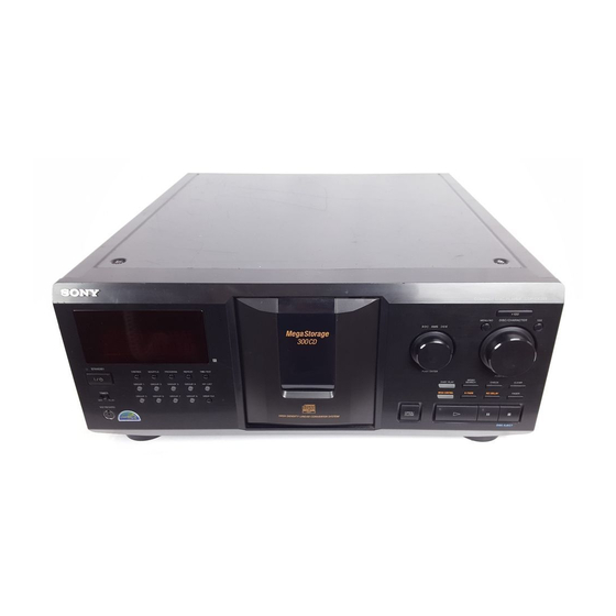
Photo; CDP-CX350
Model Name Using Similar Mechanism
CD Mechanism Type
Base Unit Type
Optical Pick-up Type
SPECIFICATIONS
– 1 –
US Model
CDP-CX300/CX350/CX691
Canadian Model
CDP-CX300/CX350
AEP Model
UK Model
Australian Model
NEW
CDM54-KIBD35E
KSM-213BFN/M-NP
KSS-213BFN
COMPACT DISC PLAYER
CDP-CX350
Advertisement
Table of Contents

Related Manuals for Sony CDP-CX300


Summary of Contents for Sony CDP-CX300
- Page 1 CDP-CX300/CX350/CX691 SERVICE MANUAL US Model CDP-CX300/CX350/CX691 Canadian Model CDP-CX300/CX350 AEP Model UK Model Australian Model CDP-CX350 Photo; CDP-CX350 Model Name Using Similar Mechanism CD Mechanism Type CDM54-KIBD35E Base Unit Type KSM-213BFN/M-NP Optical Pick-up Type KSS-213BFN SPECIFICATIONS COMPACT DISC PLAYER MICROFILM...
- Page 2 DES PIÈCES SONT CRITIQUES POUR LA SÉCURITÉ DE 4-215-964-7π CX691 : US FONCTIONNEMENT. NE REMPLACER CES COMPOSANTS • Abbreviation QUE PAR DES PIÈCES SONY DONT LES NUMÉROS CND : Canadian model SONT DONNÉS DANS CE MANUEL OU DANS LES AUS : Australian model SUPPLÉMENTS PUBLIÉS PAR SONY.
-
Page 3: Table Of Contents
SECTION 1 SERVICING NOTE TABLE OF CONTENTS NOTES ON HANDLING THE OPTICAL PICK-UP BLOCK OR BASE UNIT 1. SERVICING NOTE ............3 The laser diode in the optical pick-up block may suffer electrostatic 2. GENERAL ................6 break-down because of the potential difference generated by the charged electrostatic load, etc. - Page 4 CD-TEXT TEST DISC This unit is able to display the TEXT data (character information) written in the CD on its fluorescent indicator tube. The CD-TEXT TEST DISC (TGCS-313:J-2501-126-A) is used for checking the display. To check, perform the following procedure. Checking Method: 1.
- Page 5 Table 2: CD-TEXT TEST DISC Recorded Contents and Display (In this unit, some special characters cannot be displayed. This is no a fault.) TRACK Display Recorded contents N All the same ! ” # $ % & ´ (21h to 27h)1kHz 0dB L&R N All the same + , –...
-
Page 6: General
SECTION 2 GENERAL Front Panel 4 5 6 7 8 11 12 15 16 17 18 19 20 21 22 36 35 34 33 32 31 30 29 28 27 Photo: CDP-CX350 LOCATION OF PARTS AND CONTROLS 1 1/u (power) button 21 NO DELAY button 2 STANDBY indicator 22 FADER button... -
Page 7: Disassembly
SECTION 3 DISASSEMBLY Note : Follow the disassembly procedure in the numerical order given. 3-1. FRONT PANEL ASSEMBLY 6 Flat tayp wire(CN701) 4 Remove the claw 3 Two screw (BVTP 3x8) 1 Two screws (BVTP 3x8) 5 Remove the claw 7 Front panel assembly 2 Three screws (BVTP 3x8) 3-2. -
Page 8: Base (Door, Gear) Assembly
3-3. BASE (DOOR, GEAR) ASSEMBLY 1 Two screws (BVTP 3x8) Two screws (BVTP 3x8) Connector (CN508) !™ Base (door.gear) assembly Cover(P.T.) 2 Cover(front) 3 Three screws (BVTP 3x8) 4 Guide (Door.B) 6 Bracket (Guide.B) 0 Two screws (BVTP 3x8) 5 Four screws (BVTP 3x8) !¡... - Page 9 3-5. BACK PANEL ASSEMBLY 6 Two screws (BVTP 3x8) 7 Two screws (BVTP 3x8) 0 Back panel 8 Two screws !¡ Two screws (BVTP 3x8) (BVTP 3x8) !£ Main board 4 Connector (CN84) 3 Connector 5 Three screws (CN901) (BVTP 3x8) 2 Connector 9 Guide (main) (CN903)
-
Page 10: Service Mode
SECTION 4 SERVICE MODE SPECIAL FUNCTION This unit is provided with several service modes. Details are shown in the following table. Mode name Power supply state Button operation Remarks ALL ERASE CLEAR + Note 1 AGING MODE GROUP 1 + OPEN/CLOSE + +100 §... - Page 11 Special Aging Mode Functions Aging Procedure 1. Turn ON the power of the unit. Press the § OPEN/CLOSE and The aging mode is provided with the following convenient func- tions open the front cover. • Disc setting mode (*1) 2. Change the COMMAND MODE switch (S901) on set to CD1 . •...
- Page 12 LOADING AGING MODE TABLE ROTATION MODE • This mode is used for repeating loading operations continuously. • This mode is used for electrical adjustments. Refer to the section • Aging will be performed continuously unless an error occurs. on Electrical Adjustments. •...
- Page 13 MECHANISM ADJUSTMENT MODE • This mode is used for mechanism adjustments. Refer to the sec- tion on Mechanism Adjustments. SHIPMENT MODE • This mode is used for setting the unit to the shipment state. Do not execute it without a proper reason as it erases the memory of the title memo recorded by the customer.
-
Page 14: Test Mode
SECTION 5 TEST MODE 5-1. ADJ MODE 5-2. KEY AND DISPLAY CHECK MODE 1. Turn ON the power of the unit, set disc to disc table, and per- To set this mode, connect the test point (AFADJ) on the MAIN form chucking. -
Page 15: Adjustments
SECTION 6 ADJUSTMENTS 6-1. MECHANICAL ADJUSTMENTS Pop Up Mechanism Adjustment GROUP1 1. With the power ON, while pressing the GROUP 4 and · GROUP2 buttons, press the +100 button to enter the mechanism adjust- GROUP4 ment mode. 2. Press the GROUP 1 button to operate the loading mechanism, and continue pressing until the disc table locks. - Page 16 Sensor Adjustment 1. With the power ON, while pressing the GROUP 4 and · GROUP1 buttons, press the +100 button to enter the mechanism adjust- PAUSE button ment mode. GROUP4 2. Press the GROUP 1 button to operate the loading mechanism, PLAY button and continue pressing until the disc table locks.
-
Page 17: Electrical Adjustment
6-2. ELECTRICAL ADJUSTMENT Note: A clear RF signal waveform means that the shape “ ” can be clearly distinguished at the center of the waveform. Note: RF signal waveform 1. CD Block is basically designed to operate without adjustment. Therefore, check each item in order given. VOLT/DIV : 200mV TIME/DIV : 500ns 2. - Page 18 Disc Sensor Adjustment 5. Rotate the DISC/CHARACTER knob in the counterclockwise Be sure to perform this adjustment after sensor adjustment in ME- direction and the disc table starts to rotate in the same direction. CHANICAL ADJUSTMENT. Check that the waveform at this time is the same as that in step 4.
- Page 19 Adjustment Location : [ BD BOARD ] – Side B – IC102 (FE1) (RF) (TE) IC103 (VC) [ MAIN BOARD ] – Component Side – CN506 RV501 DISC SENSOR IC502 ADJUSTMENT 12 11 TP2 (AFADJ) R516 TP1 (ADJ) R517 – 19 –...
-
Page 20: Diagrams
SECTION 7 DIAGRAMS 7-1. CIRCUIT BOARDS LOCATION JACK board LED board T . SENS board MAIN board D . SENS (OUT) board DISPLAY board KEY board POWER board D . SENS (IN) board D . SW board D . MOTOR board JOG board BD board SW board... -
Page 21: Block Diagrams
CDP-CX300/CX350/CX691 7-2. BLOCK DIAGRAMS – BD SECTION – IC101 DIGITAL SIGNAL PROCESSOR OPTICAL PICK-UP IC103 BLOCK (KSS-213B) RF AMP LASER DIODE POWER IC901 APC LD DIGITAL DOUT DIGITAL OPTICAL DRIVE ASYO Q101 DETECTOR RFAC RF EQ SUMMING ASYI ASYMMETRY DIGITAL... -
Page 22: Main Section
CDP-CX300/CX350/CX691 – MAIN SECTION – FL701 D940 D942 –30V REG RECTIFIER J903 Q940 MUTE 2ND CD IN IC910 Q324 L901 5V REG IC401 RECT LINE AC IN IC302(1/2) IC302(2/2) D910-913 FILTER –VCC MIX AMP IC920 LOUT MUTE Q321 7V REG... - Page 23 CDP-CX300/CX350/CX691 WAVEFORMS THIS NOTE IS COMMON FOR PRINTED WIRING BOARDS AND SCHEMATIC DIAGRAMS. (In addition to this, the necessary note is printed in each block.) 3.1Vp-p For schematic diagrams. 16.9MHz Note: IC101 ^¶ XTAI • All capacitors are in µF unless otherwise noted. pF: µµF 50 WV or less are not indicated except for electrolytics and tantalums.
-
Page 24: Schematic Diagram - Bd Section
CDP-CX300/CX350/CX691 7-3. SCHEMATIC DIAGRAM – BD SECTION – • See page 26 for Waveforms. • See page 53, 54 for IC Block Diagrams. • See page 56 for IC Pin Functions. (Page 36) – 27 – – 28 –... -
Page 25: Printed Wiring Board - Bd Section
CDP-CX300/CX350/CX691 7-4. PRINTED WIRING BOARD – BD SECTION – • See page 20 for Circuit Boards Location. (Page 32) – 30 – – 29 –... -
Page 26: Printed Wiring Board - Main Section
CDP-CX300/CX350/CX691 7-5. PRINTED WIRING BOARD – MAIN SECTION – • See page 20 for Circuit Boards Location. (Page 48) (Page 48) (Page 52) (Page 52) (Page 37) (Page 30) (Page 41) (Page 52) • Semiconductor Location Ref. No. Location Ref. No. -
Page 27: Schematic Diagram - Main (1/2) Section
CDP-CX300/CX350/CX691 7-6. SCHEMATIC DIAGRAM – MAIN (1/2) SECTION – • See page 26 for Waveforms. • See page 58 for IC Pin Functions. • See page 54, 55 for IC Block Diagrams. (Page 51) (Page 51) (Page 51) (Page 51) -
Page 28: Schematic Diagram - Main (2/2) Section
CDP-CX300/CX350/CX691 7-7. SCHEMATIC DIAGRAM – MAIN (2/2) SECTION – • See page 20 for Waveforms. • See page 58 for IC Pin Functions. • See page 54, 55 for IC Block Diagrams. (Page 27) (Page 47) (Page 47) (Page 49) (Page 49) –... -
Page 29: Printed Wiring Board - T.sens Section
CDP-CX300/CX350/CX691 7-8. PRINTED WIRING BOARD – T.SENS SECTION – 7-11. SCHEMATIC DIAGRAM – SENSOR SECTION – • See page 20 for Circuit Boards Location. • See page 26 for Waveforms. (Page 32) 7-9. PRINTED WIRING BOARD – D.SENS (IN) SECTION –... -
Page 30: Schematic Diagram - Display Section
CDP-CX300/CX350/CX691 7-12. SCHEMATIC DIAGRAM – DISPLAY SECTION – • See page 26 for Waveforms. (Page 44) (Page 51) (Page 34) – 40 – – 39 –... -
Page 31: Printed Wiring Board - Display Section
CDP-CX300/CX350/CX691 7-13. PRINTED WIRING BOARD – DISPLAY SECTION – • See page 20 for Circuit Boards Location. (Page 46) (Page 32) • Semiconductor Location Ref. No. Location D701 D702 D703 D704 D705 D706 D707 D708 D709 D710 D771 D772 D773... -
Page 32: Schematic Diagram - Jog Section
CDP-CX300/CX350/CX691 7-14. SCHEMATIC DIAGRAM – JOG SECTION – • See page 26 for Waveforms. (Page 39) p/DISC EJECT – 43 – – 44 –... -
Page 33: Printed Wiring Board - Jog Section
CDP-CX300/CX350/CX691 7-15. PRINTED WIRING BOARD – JOG SECTION – • See page 20 for Circuit Boards Location. • Semiconductor Location Ref. No. Location D771 D712 D713 D714 D715 D716 (Page 41) p/DISC EJECT – 45 – – 46 –... -
Page 34: Schematic Diagram - Power Section
CDP-CX300/CX350/CX691 7-16. SCHEMATIC DIAGRAM – POWER SECTION – 7-17. PRINTED WIRING BOARD – POWER SECTION – • See page 26 for Waveforms. • See page 20 for Circuit Boards Location. (Page 35) (Page 32) (Page 35) (Page 31) • Semiconductor Location Ref. -
Page 35: Schematic Diagram - Jack Section
CDP-CX300/CX350/CX691 7-18. SCHEMATIC DIAGRAM – JACK SECTION – 7-19. PRINTED WIRING BOARD – JACK SECTION – • See page 26 for Waveforms. • See page 20 for Circuit Boards Location. (Page 36) (Page 36) (Page 32) (Page 32) – 50 –... -
Page 36: Schematic Diagram - Sensor/Motor Section
CDP-CX300/CX350/CX691 7-21. PRINTED WIRING BOARD – SENSOR/MOTOR SECTION – 7-20. SCHEMATIC DIAGRAM – SENSOR/MOTOR SECTION – • See page 20 for Circuit Boards Location. (Page 34) (Page 31) (Page 31) (Page 32) (Page 34) (Page 40) (Page 33) (Page 42) -
Page 37: Ic Block Diagrams
7-22. IC BLOCK DIAGRAMS • BD section IC101 CXD2587Q ERROR DIGITAL CORRECTOR DIGITAL ASYMMETRY CORRECTION OPERATIONAL LRCK AMPLIFIER ANALOG SWITCH PCMD INTERFACE DEMODULATOR CONVERTER EMPH XVDD XTAI TIMING LOGIC CLOCK XTAO XTSL GENERATOR XVSS TES1 AVDD1 TEST AOUT1 SERVO DSP PWM GENERATOR AIN1 FRDR... - Page 38 IC103 CXA2568M-T6 APC PD AMP LC/PD LD_ON HOLD AGCVTH VREF APC LD AMP HOLD_SW AGCCONT (50%/30% OFF) RF_BOT RFTC RF SUMMING AMP RF_EQ_AMP RF_1 ERROR AMP FOCUS TRACKING ERROR AMP VC BUFFER • Main section IC504 M5M5256DFP-70XL INPUT DATA CONTROL OUTPUT BUFFER CLOCK...
-
Page 39: Display Section
IC505 LA6510 IC931 LA5601 – – V REF 1 2 3 4 5 6 7 8 9 10 VOMUTE RESET ON/OFF • Display section IC702 M66310FP – 55 –... -
Page 40: Ic Pin Functions
7-23. IC PIN FUNCTIONS • IC101 DIGITAL SIGNAL PROCESSOR (CXD2587Q) (BD board) Pin Name Function Pin No. SQSO Sub-Q 80-bit and PCM peak level data output (CD text data output) SQCK Clock input for SQSO read-out XRST System reset “L” : reset SYSM Muting input “H”... - Page 41 Pin No. Pin Name Function Tracking error signal input Center servo analog input RFDC RF signal input Test pin (Not used) ADIO – Analog ground AVSS0 Stabilized current input for operational amplifiers IGEN – Analog power supply AVDD0 EFM full swing output ASYO Asymmetry comparate voltage input ASYI...
- Page 42 • IC501 SYSTEM CONTROL (MN101C12G-SA) (MAIN board) Pin Name Function Pin No. — Ground DOOR SW Door panel SW (5V: OPEN) FILTER SW D-F mode change SW KEY1 KEY2 KEY3 Key A/D input KEY4 KEY5 D.SENS — Disc sensor input VREF —...
- Page 43 Pin Name Function Pin No. LED1 interior illumination SELECT CX691 select port (H: CX691 L: Other) Table sensor input SELECT J select port (H: J L: Other) SELECT ES select port (H: ES L: HiFi) (Fix at L) SELECT 2WAY select port (H: 2WAY L: ONE WAY) 2WAY-LT U-COM chip enable output CX5/CX6...
-
Page 44: Exploded Views
SECTION 8 EXPLODED VIEWS NOTE: The components identified by • The mechanical parts with no reference number in • -XX, -X mean standardized parts, so they may have mark ! or dotted line with mark the exploded views are not supplied. some difference from the original one. -
Page 45: Chassis Section
8-2. CHASSIS SECTION not supplied not supplied not supplied not supplied not supplied Ref. No. Part No. Description Remark Ref. No. Part No. Description Remark X-4950-889-1 DOOR (CD) ASSY 4-216-091-01 HOLDER (TABLE SENSOR) X-4950-902-1 TABLE (300) ASSY 4-216-092-01 HOLDER (ROLLER) 4-215-952-01 GUIDE (DOOR.B) 4-216-093-01 ROLLER 4-215-953-01 GUIDE (DOOR.T) -
Page 46: Front Panel Section
1-790-420-11 WIRE (FLAT TYPE) (21 CORE) A-4724-546-A DISPLAY BOARD, COMPLETE (CX350) X-4950-917-1 PANEL ASSY, FRONT (CX691) A-4724-566-A DISPLAY BOARD, COMPLETE (CX300/CX691) 4-996-698-01 EMBLEM, SONY A-4724-545-A JOG BOARD, COMPLETE (CX350) 4-215-928-01 BUTTON (POWER) 3-917-216-21 KNOB (TIMER) A-4724-565-A JOG BOARD, COMPLETE (CX300/CX691) -
Page 47: Mechanism Section 1 (Cdm54-K1Bd35E)
8-4. MECHANISM SECTION 1 (CDM54-K1BD35E) Ref. No. Part No. Description Remark Ref. No. Part No. Description Remark X-4950-888-1 BRACKET (DOOR.GEAR) ASSY 1-672-634-11 D.SW (A) BOARD 4-215-959-01 LEVER (CAM.PU) 4-216-099-01 SLIDER (POP-UP) 4-215-955-01 GEAR (DOOR.PULLEY) 4-216-100-01 HOLDER (POP-UP) 4-215-956-01 GEAR (DOOR.CENTER) 4-216-098-01 LEVER (POP-UP) 4-215-957-01 GEAR (DOOR.DRIVE) 3-701-441-21 WASHER... -
Page 48: Mechanism Section 2 (Cdm54-K1Bd35E)
8-5. MECHANISM SECTION 2 (CDM54-K1BD35E) Ref. No. Part No. Description Remark Ref. No. Part No. Description Remark 4-216-054-01 BASE (CDM) 4-216-081-01 SPRING (MG), TORSION 4-216-063-01 SLIDER 4-998-716-01 SCREW, BU FITTING 1-672-636-11 L.T.MOTOR BOARD 3-701-446-21 WASHER, 8 1-672-642-11 SW BOARD 1-672-643-11 SW2 BOARD A-4672-676-A CAM ASSY 4-216-062-01 LEVER (FULCRUM) 4-216-061-01 BELT... -
Page 49: Mechanism Section 3 (Cdm54-K1Bd35E)
8-6. MECHANISM SECTION 3 (CDM54-K1BD35E) not supplied Ref. No. Part No. Description Remark Ref. No. Part No. Description Remark X-4950-900-1 BRACKET (LEVER) ASSY 4-216-067-01 SPRING (CLAMP), COMPRESSION 3-325-697-21 WASHER 4-216-070-01 LEVER (LOCK) 4-216-075-01 HOLDER (F) 4-957-577-01 SCREW PTP WH (2.6X8) (DIA. 10) 4-216-076-01 HOLDER (R) 4-216-077-01 SPRING (HOLDER FR), TORSION 4-216-086-01 SPRING (F-2), TENSION... -
Page 50: Opeical Pick-Up Section (Ksm-213Bfn/M-Np)
8-7. OPTICAL PICK-UP SECTION (KSM-213BFN/M-NP) not supplied M102 M101 Les composants identifiés par une The components identified by marque ! sont critiques pour la mark ! or dotted line with mark ! are critical for safety. sécurité. Replace only with part number Ne les remplacer que par une specified. -
Page 51: Electrical Parts List
SECTION 9 ELECTRICAL PARTS LIST Note: • Due to standardization, replacements in the parts list • SEMICONDUCTORS The components identified by In each case, u: µ , for example: may be different from the parts specified in the mark ! or dotted line with mark uA...: µ... - Page 52 D. MOTOR D. SENS (IN) D. SENS (OUT) D. SW DISPLAY Ref. No. Part No. Description Remark Ref. No. Part No. Description Remark R138 1-216-295-91 SHORT < SWITCH > R143 1-216-103-00 METAL CHIP 180K 1/10W R144 1-216-103-00 METAL CHIP 180K 1/10W SW83 1-571-300-21 SWITCH, ROTARY...
- Page 53 DISPLAY JACK Ref. No. Part No. Description Remark Ref. No. Part No. Description Remark D780 8-719-911-19 DIODE 1SS119 (CX350) R775 1-247-772-00 CARBON 1/4W D781 8-719-911-19 DIODE 1SS119 (CX350) (CX350) D782 8-719-911-19 DIODE 1SS119 (CX350) R776 1-247-772-00 CARBON 1/4W (CX350) < GROUND TERMINAL > R791 1-249-429-11 CARBON 1/4W...
- Page 54 JACK Ref. No. Part No. Ref. No. Description Part No. Description Remark Remark < RESISTOR > RE702 1-475-543-11 ENCODER, ROTARY (DISC/CHARACTER PUSH ENTER) R339 1-215-485-00 METAL 470K 1/4W R340 1-215-405-00 METAL 1/4W < SWITCH > R439 1-215-485-00 METAL 470K 1/4W R440 1-215-405-00 METAL 1/4W...
- Page 55 L.T. MOTOR MAIN Ref. No. Part No. Description Remark Ref. No. Part No. Description Remark 1-672-636-11 L.T. MOTOR BOARD C510 1-161-494-00 CERAMIC 0.022uF C511 1-161-494-00 CERAMIC 0.022uF *************** C512 1-161-494-00 CERAMIC 0.022uF < MOTOR > C514 1-164-159-11 CERAMIC 0.1uF C516 1-164-159-11 CERAMIC 0.1uF 1-541-632-11 MOTOR, DC (TABLE)
- Page 56 MAIN Ref. No. Part No. Description Remark Ref. No. Part No. Description Remark CN504 1-506-469-11 PIN, CONNECTOR 4P Q521 8-729-030-08 TRANSISTOR DTC144VSA-TP Q550 8-729-900-89 TRANSISTOR DTC144ES CN505 1-506-469-11 PIN, CONNECTOR 4P Q551 8-729-900-65 TRANSISTOR DTA144ES * CN506 1-564-518-11 PLUG, CONNECTOR 3P Q552 8-729-900-65 TRANSISTOR DTA144ES * CN507...
- Page 57 MAIN POWER Ref. No. Part No. Description Remark Ref. No. Part No. Description Remark R411 1-215-445-00 METAL 1/4W R557 1-249-382-11 CARBON 1/6W F R412 1-215-445-00 METAL 1/4W R413 1-215-477-00 METAL 220K 1/4W R558 1-247-807-31 CARBON 1/4W R559 1-249-419-11 CARBON 1.5K 1/4W F R414 1-215-405-00 METAL...
- Page 58 POWER T. SENS Ref. No. Part No. Description Remark Ref. No. Part No. Description Remark C937 1-126-960-11 ELECT IC83 8-749-924-18 IC PHOTO INTERRUPTER RPI-1391 (TABLE SENSOR) < CONNECTOR > IC84 8-749-924-18 IC PHOTO INTERRUPTER RPI-1391 (TABLE SENSOR) * CN991 1-580-230-11 PIN, CONNECTOR (PC BOARD) 2P <...
- Page 59 Ref. No. Part No. Description Remark ACCESSORIES & PACKING MATERIALS ******************************* 1-418-254-11 REMOTE COMMANDER (RM-DX350) (CX350) 1-418-419-11 COMMANDER, REMOTE (RM-DX300) (CX300) 1-776-263-11 CORD, CONNECTION (AUDIO) 1-777-172-11 CORD, CONNECTION (CONTROL A1:CND) 3-810-765-11 MANUAL,COMMONNESS INSTRUCTION (FOR CONTROL A1) (CX300:US/CX350:US/CX691) 3-810-765-21 MANUAL,COMMONNESS INSTRUCTION (FOR CONTROL A1) (CX300:CND/CX350:CND,AEP,UK,AUS) 3-866-362-11 MANUAL, INSTRUCTION (ENGLISH) (CX300/CX691)
- Page 60 CDP-CX300/CX350/CX691 Sony Corporation 99D0974-1 Printed in Japan © 1999. 4 9-928-884-11 Home A&V Products Company Published by Quality Assurance Dept. – 76 – (Shinagawa)