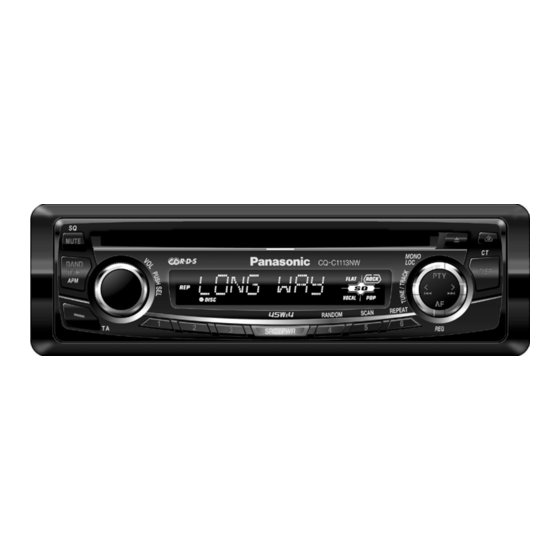
Panasonic CQ-C1113NW Service Manual
Removable front panel cd player/receiver
Hide thumbs
Also See for CQ-C1113NW:
- Operating instructions (4 pages) ,
- Operating instructions (2 pages)
Table of Contents
Advertisement
Quick Links
Specifications*
General
Power Supply
Tone Controls
Current Consumption
Maximum Power Output
Suitable Speaker Impedance
FM Stereo Radio
Frequency Range
Usable Sensitivity
AM Radio
Frequency Range
Usable Sensitivity
RDS
DC 12V (11V - 16V),
Test Voltage 14.4V
Negative Ground
Bass ; ±12dB at 100Hz
Treble ; ±12dB at 10kHz
Less than 2.2A (CD play mode,
0.5W×4ch)
45W×4ch (at 1kHz, Vol. Max.)
4-8Ω
87.5 - 108MHz
11.0dBf (1.25µV, 75Ω)
531 - 1,602kHz
28dB/µV (25µV, S/N 20dB)
AUTOMOTIVE AFTERMARKET
CQ-C1113NW
Removable Front Panel CD Player /
Receiver
RDS Sensitivity
CD Player
Sampling Frequency
Pick-Up Type
Light Source
Wavelength
Frequency Response
Signal to Noise Ratio
Dimensions**
Weight**
* Specifications and the design are subject to possible modification
without notice due to improvements.
** Dimensions and Weight shown are approximate.
© 2005 Matsushita Electric Industrial Co., Ltd. All
rights
reserved.
distribution is a violation of law.
Order No. ACED051207C8
22dB/µV
8 times oversampling
Astigma 3-beam
Semiconductor Laser
780nm
20Hz to 20,000Hz (±1dB)
96dB
178×50×155mm
1.4kg
Unauthorized
copying
and
Advertisement
Table of Contents

Related Manuals for Panasonic CQ-C1113NW


Summary of Contents for Panasonic CQ-C1113NW
- Page 1 Order No. ACED051207C8 AUTOMOTIVE AFTERMARKET CQ-C1113NW Removable Front Panel CD Player / Receiver Specifications* General RDS Sensitivity 22dB/µV Power Supply DC 12V (11V - 16V), Test Voltage 14.4V CD Player Negative Ground Sampling Frequency 8 times oversampling Tone Controls Bass ; ±12dB at 100Hz...
-
Page 2: Table Of Contents
CQ-C1113NW CONTENTS Page Page 1 ABOUT LEAD FREE SOLDER (PbF) 11 PACKAGE AND IC BLOCK DIAGRAM 2 FEATUERS 12 REPLACEMENT PARTS LIST 3 LASER PRODUCTS 13 EXPLODED VIEW (Unit) 4 REPLACEING THE FUSE 14 CD PLAYER MECHANICAL PARTS LIST 5 MAINTENANCE... -
Page 3: Maintenance
CQ-C1113NW 5 MAINTENANCE Your products is designed and manufactured to ensure a minimum of maintenance. Use a dry, a soft cloth for routine exterior cleaning. Never use benzine, thinner or other solvents. 6 NOTES [RADIO BLOCK] Do not align the AM/FM package block. When the package block is necessary, it will be supplied already aligned at the factory. -
Page 4: Wiring Connection
CQ-C1113NW 8 WIRING CONNECTION... -
Page 5: Block Diagram
CQ-C1113NW 9 BLOCK DIAGRAM... -
Page 6: Terminals Description
CQ-C1113NW 10 TERMINALS DESCRIPTION 10.1. Main Block IC601 : LC7237849D08 Ref. Part Part Name & Description I/O(V) FM(V AM(V CD(V Ref. Part Part Name & Description I/O(V) FM(V AM(V CD(V N.C. None N.C. None X’tal 2.52 2.53 2.52 BZ_OUT Connection... - Page 7 CQ-C1113NW Pin No. Port Descriptions TEST (Connecting to ground) +5V power supply VDD1 Ground through capacitor VDD2 Ground through capacitor Ground CR oscillator Key data output Chip enable LCD clock LCD data input...
-
Page 8: Package And Ic Block Diagram
CQ-C1113NW 11 PACKAGE AND IC BLOCK DIAGRAM 11.1. Main Block P50:J3CCBC000010 IC270 : C1EA00000042... - Page 9 CQ-C1113NW IC1 : C1BB00001089...
- Page 10 CQ-C1113NW IC300 : C1BB00000543 IC2 : C1BB00001088...
- Page 11 CQ-C1113NW IC701 : C0DAZHF00004 IC201 : C1BB00000960...
-
Page 12: Replacement Parts List
CQ-C1113NW 12 REPLACEMENT PARTS LIST Ref. Part No. Part Name & Description Remarks D968 YEAD1N4005ST Silicon Diode DISPLAY BLOCK [E-4C292] D901 YEADSPADB01 LED (BLUE) D902 YEADSPADR01 LED (RED) D903 YEADSPADR01 LED (RED) D905 YEADSPADR01 LED (RED) D906 YEADSPADR01 LED (RED) - Page 13 CQ-C1113NW Ref. Part No. Part Name & Description Remarks Ref. Part No. Part Name & Description Remarks F1J1H153A733 Ceramic 0.015MFD 50WV XL01 YEXL16M9X54A Ceramic Filter F1K1E223A069 Ceramic 0.022MFD 25WV F1J1H123A733 Ceramic 0.012MFD 50WV DISPLAY BLOCK [E-4C292] F1J1H682A733 Ceramic 6800pF 50WV...
- Page 14 CQ-C1113NW Ref. Part No. Part Name & Description Remarks Ref. Part No. Part Name & Description Remarks J335 ERJ8GX0R00V Chip 0 ohms 1/8W D0AZ102JA008 Chip 1k ohms 1/6W J336 ERJ8GX0R00V Chip 0 ohms 1/8W ERJ8GEYJ5R6V Chip 5.6 ohms 1/8W J337...
- Page 15 CQ-C1113NW Ref. Part No. Part Name & Description Remarks Ref. Part No. Part Name & Description Remarks R702 D0GD153JA017 Chip 15k ohms 1/10W SW913 K0H1BA000445 Tack Swich R703 D0AE102JA131 Chip 1k ohms 1/4W SW914 K0H1BA000445 Tack Swich R704 D0AE471JA131 Chip 470 ohms 1/4W...
- Page 16 CQ-C1113NW Ref. Part No. Part Name & Description Remarks XTN2+8GFZ Screw T(2-C) YFX054C071CA Spring (PUSH BUTTON) T(2-C) YFE134C491YA Button (Push) T(2-C) YFC034C001CA ESC Rear Cover T(2-C) YFE134C510CA Button (TUNE/TRACK)Ring T(2-B) YFV024C108CA Sheet T(2-B) YFE134C515CA Button (PTY/AF) T(1-B) YFX054C072CA Spring (OPEN)
-
Page 17: Exploded View (Unit)
CQ-C1113NW 13 EXPLODED VIEW (Unit) -
Page 18: Cd Player Mechanical Parts List
CQ-C1113NW 14 CD PLAYER MECHANICAL PARTS LIST Ref. Part No. Part Name & Description Remarks 3032 10 40 SW WIRE MN N(A-1) 3032 10 39 SP WIRE MN N(D-2) 3032 10 13 WIRE CLAMPER M N(C-2); N(C-3); N(D-4); N(E-3) 3032 10 28... -
Page 19: Exploded View (Cd Deck)
CQ-C1113NW 15 EXPLODED VIEW (CD Deck) -
Page 20: Wiring Diagram
CQ-C1113NW 16 WIRING DIAGRAM 16.1. Main Block-1 [E-4C290][TOP VIEW] CQ-C1103U/W/D/H/NE/NW CQ-C1113NE/NW CQ-C1123NE/NW MAIN PCB... - Page 21 CQ-C1113NW 16.2. Main Block-2 [E-4C290][BOTTOM VIEW] CQ-C1103U/W/NE/NW/D/H CQ-C1113NE/NW CQ-C1123NE/NW MAIN PCB...
- Page 22 CQ-C1113NW 16.3. Display Block [E-4C292][TOP VIEW] [E-4C292][BOTTOM VIEW] CQ-C1103NE/NW CQ-C1113NE/NW CQ-C1123NE/NW DISPLAY PCB...
- Page 23 CQ-C1113NW 16.4. CD Interface Block [E-4C288][BOTTOM VIEW] CQ-C1103U/W/H/D CQ-C1113NW CQ-C1333U/W CQ-C1303U/W/H/D/NE/NW CQ-C1313NE/NW CQ-C1323NE/NW CD INTERFACE PCB...
- Page 24 THIS PAGE IS JUST FOR THE PAGE LAYOUT USE ONLY.
-
Page 25: Schematic Diagram-1
CQ-C1113NW 17 SCHEMATIC DIAGRAM-1 17.1. Main Block E-4C290 2.51 5.14 0.43 5.14 2.33 2.56 2.57 2.57 8.22 8.23 4.36 0.23 0.79 2.31 1.69 0.02 0.48 8.88 8.22 8.16 0.13 1.73 5.34 5.32 5.32 0.86 CQ-C1003H/C1013H/C1113NE/C1113NW/C1123NE/1123NW/C1103H/C1103NE/C1103NW/C1103U/C1103W MAIN BLOCK... - Page 26 CQ-C1113NW 17.2. Main Block...
-
Page 27: Schematic Diagram-2
CQ-C1113NW 18 SCHEMATIC DIAGRAM-2 18.1. Display Block... - Page 28 CQ-C1113NW 18.2. CD Interface Block...
-
Page 29: Schematic Diagram For Printing With A4 Size
CQ-C1113NW 19 SCHEMATIC DIAGRAM for printing with A4 size 19.1. Main Block (Left Side) E-4C2 2.51 5.14 5.14 2.33 2.56 2.57 2.57 8.22 8.23 4.36 2.31 0.79 1.69 0.02 8.88 8.22 8.16 0.13 1.73... - Page 30 CQ-C1113NW 19.2. Main Block (Right Side) E-4C290 0.43 0.23 0.48 5.34 5.32 5.32 0.86 CQ-C1003H/C1013H/C1113NE/C1 113NW/C1123NE/1 123NW/C1103H/C1103NE/C1 103NW/C1103U/C1103W MAIN BLOCK Printed in Taiwan 2005.11...