Table of Contents
Advertisement
Quick Links
ORDER NO. KMS0308820C1
F19
16Port Single Line Telephone Extension Card
KX-TDA0174
(for U.S.A.)
2003 Panasonic Communications Co., Ltd. All rights reserved.
Unauthorized copying and distribution is a violation of law.
IMPORTANT INFORMATION ABOUT LEAD FREE, (PbF), SOLDERING
If lead free solder was used in the manufacture of this product the printed circuit boards will be
marked PbF.
Standard leaded, (Pb), solder can be used as usual on boards without the PbF mark.
When this mark does appear please read and follow the special instructions described in this
manual on the use of PbF and how it might be permissible to use Pb solder during service and
repair work.
1. ABOUT LEAD FREE SOLDER (PbF: Pb free)
Note:
In the information below, Pb, the symbol for lead in the periodic table of elements, will refer to
1
Advertisement
Table of Contents

Related Manuals for Panasonic KX-TDA0174

Summary of Contents for Panasonic KX-TDA0174
- Page 1 16Port Single Line Telephone Extension Card KX-TDA0174 (for U.S.A.) 2003 Panasonic Communications Co., Ltd. All rights reserved. Unauthorized copying and distribution is a violation of law. IMPORTANT INFORMATION ABOUT LEAD FREE, (PbF), SOLDERING If lead free solder was used in the manufacture of this product the printed circuit boards will be marked PbF.
-
Page 2: Suggested Pbf Solder
standard solder or solder that contains lead. We will use PbF solder when discussing the lead free solder used in our manufacturing process which is made from Tin, (Sn), Silver, (Ag), and Copper, (Cu). This model, and others like it, manufactured using lead free solder will have PbF stamped on the PCB. -
Page 3: How To Recognize That Pb Free Solder Is Used
1.2. HOW TO RECOGNIZE THAT Pb FREE SOLDER IS USED “PbF” is marked on the PCB to show that Pb free solder is used.(See the figure below.) -
Page 4: For Service Technicians
2. FOR SERVICE TECHNICIANS ICs and LSIs are vulnerable to static electricity. When repairing, the following precautions will help prevent recurring malfunctions. -
Page 5: General Description
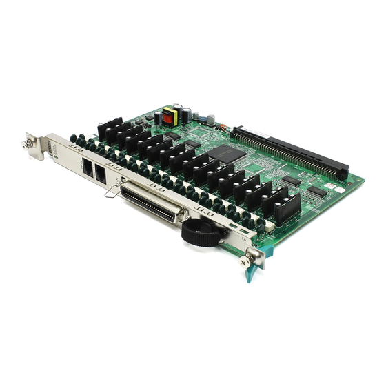
4. Do not touch IC or LSI pins with bare fingers. 3. GENERAL DESCRIPTION KX-TDA0174 (SLC16) is mounted into a free slot of TDA100/200 system. Up to 16 SLT can be randomly connected by using SLC16 card. It does not have LPR onboard, and it is controlled completely by MPR. -
Page 6: Names And Locations
Functional Block Functional contents Self-Diagnostic Function Carried out with outsire-line interface in a pair (only one port) Speech path test, Dial pulse test, DTMF test ASIC EC bus interface function CT bus interface function Local bus interface function Time switch function, Gain controlling function Intelligent PIO function LED Display Circuit Card status indicating LED: Two colors (Red/Green) - Page 7 Card Type Slot Type Option Slot MPR Slot KX-TDA100: Free Slots 1 to 5 KX-TDA200: Free Slots 1 to 10 MPR Card CO Line Cards Extension Cards OPB3 Card CTI-LINK Card Caution: To protect the back board from static electricity, do not touch parts on the back board in the main unit and on the optional service cards.To discharge static, touch ground or wear an earthing strap.
- Page 8 User-supplied: amphenol connector Pin Assignments Amphenol Connector Signal Name Function Signal Name Function Ring port 1 Tip port 1 Ring port 2 Tip port 2 Ring port 3 Tip port 3 Ring port 4 Tip port 4 Ring port 5 Tip port 5 Ring port 6 Tip port 6...
- Page 9 Velcro tape to fix the lower part of the connector. Auxiliary Connection for Power Failure Transfer Auxiliary Connection for Power Failure Transfer When the power supply to the Hybrid IP-PBX fails, power failure transfer (PFT) switches the current connection to the Auxiliary Connection automatically. A specific SLT (determined by System Programming) will be connected to selected CO lines in the event of system power failure.
- Page 10 Note Pin assignments for ports 3 and 4 are the same as those of ports 1 and 2. Accessory and User-supplied ltems Accessory: none User-supplied: RJ11 connectors RJ11 Connector Pin Assignments for CO line Crad No. Signal Name Function Ring port 2 Ring port 1 Tip port 1 Tip port 2...
- Page 11 1. Insert the card along the guide rails. 2. Holding the card as follows, push the release lever in the direction of the arrow so that the card is made to engage with the connector on the back board securely. 3.
-
Page 12: Troubleshooting Guide
6. TROUBLESHOOTING GUIDE... - Page 19 7. BLOCK DIAGRAM 8. CIRCUIT OPERATION 8.1. IC14(ASIC) - EC bus interface Independent bus for 16bit/8MHz two-way address data multiplex. - CT bus interface Supports eight 8.192MHz highways (128 time slots). - Local TSW Exchanges the time slots between CT bus (1024ch) and local highway (64ch).
-
Page 20: Reset Circuit
- Local gain control Controls the gain of the local highway up-and-down 64ch in 1db step arbitrarily. - CODEC interface Can connect up to four Infineon-manufactured PEB2466, and is intended for enabling the line control. - GPIO interface Parallel interface that is arbitrarily and bidirectionally programmable . - Page 21 characteristic, volume level, sidetone are configured by ASIC CODEC interface DCLK, CS, DOUT, DIN. In addition, the CODEC has an internal I/O port that supports Hook detection, DTMF detection, BELL relay control and DIAG relay control. Also, it converts A/D to D/A, and 4-line- analogue signal to PCM code (É/A) in G.711 format.
-
Page 22: Power Supply
8.5. DTMF SIGNAL DETECTION Each port has its own 4ch-DTMF receiver. The receiver detects the signal using IC1 for port A through D, IC2 for port E through H, IC4 for port I through L and IC6 for port M through P. The CODEC detects the DTMF data to be effective at EST terminal=H. - Page 23 8.7. DIAL PULSE DETECTION When a telephone initiates pulse dialing, this feature detects the pulse-dialing signal.When the telephone initiates dialing, changes in voltage is detected by the RING terminal in HIC, and this information is transmitted to the HOOK terminal (Example: 3-pin IC200A) as Make=L/Break=H signal.
-
Page 24: Surge Protection
8.9. RING TRIP FEATURE When the BELL signal is sent out, the off-hook signal from a SLT is detected, and then it breaks the BELL relay.When the handset of a ringing telephone is picked up, a DC loop is formed in the sequence of "Original bell signal", "Internal electrical resistance of a telephone", "Intercom bell load resistance"... -
Page 25: Self-Diagnosis
8.11. SELF-DIAGNOSIS A self-diagnosis relay (RL201A) is installed in A port. In the normal operation mode, it breaks the self-diagnosis relay, and in the self-diagnosis mode, it makes the self-diagnosis relay. In the self-diagnostic mode, A Tip-Ring is connected to the paired Tip-Ring of the outside-line card via backboard, and self-diagnosis is feasible.The self-diagnosis of the outside-line card includes outside call pick up, dial pulse transmission, DTMF transmission, BELL reception and CPC detection. - Page 26 8.13. BELL SIGNAL GENERATOR Bell signal for ringing an SLT is generated by amplifying the 20 or 25Hz square wave provided from MPR card to AC75Vrms onboard. The SW power supply in the BELL circuit generates between +160V and 100V of voltage by switching the +40V form the power source at 125KHz frequencies.
- Page 27 8.15. POWER SUPPLY VOLTAGE GENERATOR The input from the main power supply is in 3 voltage levels: +15V, +30V, +40V. Since the voltage levels: +15V, +5V, +3.3V, +40V, +160V, +100V, -100V and AC 75V are required onboard, voltage levels are generated onboard as written below. A DC-DC converter that generates +3.3V and +5V from 15V input from the main power supply.It consists of a circuit that steps down the voltage from +15V to +3.3V by the switching power supply of IC10, Q13 and L10, and a circuit that steps down the voltage from +15V to +5V by the...
- Page 28 switching power supply of IC7, Q12 and L7.As protective circuits, IP4 that protects from +3.3V short circuit, IP5 that protects from +5V short circuit, and an overvoltage protection that breaks IP1 by turning on FET in Q14 when a rise in voltage of +3.3V/+5V is detected. 8.16.
- Page 29 ADDRESS PIN No. SIGNAL NAME DESCRIPTIONS NOTES xxx1180 Used as "DTMF R OUTPUT ENABLED" xxx1181 VER5 H/L Card recognition (Reserved) VER4 VER3 VER2 H/L Hardware version managementInitial No. =0 VER1 VER0 PORT1 Port No. 16 PORT0...
- Page 30 ADDRESS PIN No. SIGNAL NAME DESCRIPTIONS NOTES xx1182 PF_RLY Power failure direct connection switch MWPOW1 MWPOW0 LED_G Green LED ON LED_R RED LED ON BELL CNT Bell relay stop HIGH (Fixed) xxx1183 HIGH(Fixed) HIGH(Fixed) HIGH(Fixed) HIGH(Fixed) HIGH(Fixed) HIGH(Fixed) HIGH(Fixed) HIGH(Fixed) xxx1184 Used as "DTMF R OUTPUT ENABLED"...
- Page 31 CODEC EXTENTION PIN No. SIGNAL DESCRIPTIONS NOTES PORT NAME EXT0 SO1_1 L (Fixed) CODECIC201 SO1_0 BELL0 Ringer output SB1_2 +5V pull up SB1_1 DIAG_RLY0 Self diagnosis switching SB1_0 +5V pull up SI1_1 HOOK0 Off-hook detection SI1_0 DT_EST0 DTMF detection EXT1 SO2_1 L(Fixed) SO2_0...
- Page 32 CODEC EXTENTION PIN No. SIGNAL DESCRIPTIONS NOTES PORT NAME EXT4 SO1_1 L (Fixed) CODECIC202 SO1_0 BELL4 Ringer output SB1_2 +5V pull up SB1_1 SB1_0 +5V pull up SI1_1 HOOK4 Off-hook detection SI1_0 DT_EST4 DTMF detection EXT5 SO2_1 L (Fixed) SO2_0 BELL5 Ringer output SB2_2...
- Page 33 CODEC EXTENTION PIN No. SIGNAL DESCRIPTIONS NOTES PORT NAME EXT8 SO1_1 L (Fixed) CODECIC250 SO1_0 BELL8 Ringer output SB1_2 +5V pull up SB1_1 SB1_0 +5V pull up SI1_1 HOOK8 Off-hook detection SI1_0 DT_EST8 DTMF detection EXT9 SO2_1 L (Fixed) SO2_0 BELL9 Ringer output SB2_2...
-
Page 34: How To Replace A Flat Package Ic
CODEC EXTENTION PIN No. SIGNAL DESCRIPTIONS NOTES PORT NAME EXT12 SO1_1 L (Fixed) CODECIC251 SO1_0 BELL12 Ringer output SB1_2 +5V pull up SB1_1 SB1_0 +5V pull up SI1_1 HOOK12 Off-hook detection SI1_0 DT_EST12 DTMF detection EXT13 SO2_1 L (Fixed) SO2_0 BELL13 Ringer output SB2_2... -
Page 35: Removing Solder From Between Pins
Note: See ABOUT LEAD FREE SOLDER (PbF: Pb free) 10.2. PROCEDURE 1. Tack the flat pack IC to the PCB by temporarily soldering two diagonally opposite pins in the correct positions on the PCB. Be certain each pin is located over the correct pad on the PCB. 2. -
Page 36: Terminal Guide Of Ics, Transistors And Diodes
11. TERMINAL GUIDE OF ICS, TRANSISTORS AND DIODES 12. CABINET AND ELECTRICAL PARTS LOCATION... -
Page 37: Accessories And Packing Materials
13. ACCESSORIES AND PACKING MATERIALS... -
Page 39: Replacement Parts List
14. REPLACEMENT PARTS LIST 1. RTL (Retention Time Limited) Note: The marking (RTL) indicates that the Retention Time is limited for this item. After the discontinuation of this assembly in production, the item will continue to be available for a specific period of time. The retention period of availability is depends on the type of assembly, and in accordance with the laws governing parts and product retention. -
Page 40: Main Board Parts
14.1. CABINET AND ELECTRICAL PARTS LOCATION Ref. No. Part No. Part Name & Description Remarks PQDF996Z SHAFT PQHR10005Z SPACER PQUB14Z2 LEVER PSHD1088Z SCREW PSHE1106Z TAPE PSHR1238Z SPACER PSHR1272Z REVET PSMH1212X ANGLE PSUS1020Z SPRING PSUS1021Y SPRING XUC25VW RETAINING RING 14.2. ACCESSORIES AND PACKING MATERIALS Ref. - Page 41 Ref. No. Part No. Part Name & Description Remarks (ICS) C1CB00001314 C1CB00001314 C1CB00001314 C0JBAB000504 C1CB00001314 C0DBAHA00011 PSVIPST596CN IC10 PQVIS8520F33 IC11 C0ABCB000050 IC12 C0ABCB000050 IC14 C1CB00001430 IC200A EHDHA1846A IC200B EHDHA1846A IC200C EHDHA1846A IC200D EHDHA1846A IC200E EHDHA1846A IC200F EHDHA1846A IC200G EHDHA1846A IC200H EHDHA1846A IC200I EHDHA1846A...
- Page 42 Ref. No. Part No. Part Name & Description Remarks B1GHCFJJ0007 TRANSISTOR(SI) U800 B1GFAFNN0001 TRANSISTOR(SI) (DIODES) MA8075 DIODE(SI) MA8051 DIODE(SI) PFVDDGD1FP3T DIODE(SI) MA142WKTX DIODE(SI) PFVDDGD1FP3T DIODE(SI) PFVDDGD1FP3T DIODE(SI) D202A MA110 DIODE(SI) D203A MA110 DIODE(SI) D203B MA110 DIODE(SI) D203C MA110 DIODE(SI) D203D MA110 DIODE(SI) D203E...
- Page 43 Ref. No. Part No. Part Name & Description Remarks PFVF1B221SB CERAMIC FILTER PFVF1B221SB CERAMIC FILTER PFVF1B221SB CERAMIC FILTER PFVF1B221SB CERAMIC FILTER PFVF1B221SB CERAMIC FILTER PFVF1B221SB CERAMIC FILTER PFVF1B221SB CERAMIC FILTER PFVF1B221SB CERAMIC FILTER PFVF1B221SB CERAMIC FILTER PFVF1B221SB CERAMIC FILTER PFVF1B221SB CERAMIC FILTER PFVF1B221SB CERAMIC FILTER...
- Page 44 Ref. No. Part No. Part Name & Description Remarks L201D PSLQR1K102MT COIL L201E PSLQR1K102MT COIL L201F PSLQR1K102MT COIL L201G PSLQR1K102MT COIL L201H PSLQR1K102MT COIL L201I PSLQR1K102MT COIL L201J PSLQR1K102MT COIL L201K PSLQR1K102MT COIL L201L PSLQR1K102MT COIL L201M PSLQR1K102MT COIL L201N PSLQR1K102MT COIL L201O PSLQR1K102MT COIL...
- Page 45 Ref. No. Part No. Part Name & Description Remarks RL202K K6B2CGA00094 RELAY RL202L K6B2CGA00094 RELAY RL202M K6B2CGA00094 RELAY RL202N K6B2CGA00094 RELAY RL202O K6B2CGA00094 RELAY RL202P K6B2CGA00094 RELAY (VARISTORS) ZNR20A D4EAB470A005 VARISTOR ZNR20B D4EAB470A005 VARISTOR ZNR20C D4EAB470A005 VARISTOR ZNR20D D4EAB470A005 VARISTOR ZNR20E D4EAB470A005 VARISTOR...
- Page 46 Ref. No. Part No. Part Name & Description Remarks ZNR23O D4EAB470A005 VARISTOR ZNR23P D4EAB470A005 VARISTOR (COMPONENTS PARTS) D1HA1038A005 RESISTOR ARRAY, 10K D1HA1038A005 RESISTOR ARRAY, 10K D1HA1038A005 RESISTOR ARRAY, 10K D1HA1038A005 RESISTOR ARRAY, 10K D1HA1038A005 RESISTOR ARRAY, 10K RA12 EXB38V103JV RESISTOR ARRAY, 10K RA16 EXB38V103JV RESISTOR ARRAY, 10K...
- Page 47 Ref. No. Part No. Part Name & Description Remarks ERJ3GEYJ104 100K ERJ3GEYJ104 100K ERJ3GEYJ104 100K ERJ3GEYJ104 100K ERJ3GEYJ104 100K ERJ3GEYJ104 100K ERJ3GEYJ104 100K ERJ3GEYJ104 100K ERJ3GEYJ104 100K ERJ3GEYJ104 100K ERJ3GEYJ104 100K ERJ3GEYJ104 100K ERJ3GEYJ104 100K ERJ3GEYJ104 100K ERJ3GEYJ104 100K ERJ3GEYJ104 100K ERJ3GEYJ104 100K...
- Page 48 Ref. No. Part No. Part Name & Description Remarks R139 ERJ3GEYJ101 R140 ERJ3GEYJ560 R141 ERJ3GEYJ103 R143 ERJ3GEYJ470 R144 ERJ3GEYJ470 R145 ERJ3GEYJ470 R146 ERJ3GEYJ470 R148 ERJ3GEYJ103 R149 ERJ3GEYJ220 R150 ERJ3GEYJ220 R151 ERJ3GEYJ103 R152 ERJ3GEYJ220 R153 ERJ3GEYJ220 R154 ERJ3GEYJ220 R155 ERJ3GEYJ220 R156 ERJ3GEYJ220 R157 ERJ3GEYJ220...
- Page 49 Ref. No. Part No. Part Name & Description Remarks R203O ERJ1WYJ102 R203P ERJ1WYJ102 R206A PQ4R10XJ221 R207 ERJ3GEYJ220 R208 ERJ3GEYJ220 R209 ERJ3GEYJ103 R210 ERJ3GEYJ103 R211 ERJ3GEYJ103 R212 ERJ3GEYJ103 R213 ERJ3GEYJ103 R214 ERJ3GEYJ103 R215 ERJ3GEYJ103 R216 ERJ3GEYJ103 R217 ERJ3GEYJ103 R218 ERJ3GEYJ103 R219 ERJ3GEYJ103 R220 ERJ3GEYJ103...
- Page 50 Ref. No. Part No. Part Name & Description Remarks R279 ERJ3GEYJ101 R280 ERJ3GEYJ101 R281 ERJ3GEYJ101 R282 ERJ3GEYJ103 R800 ERJ3GEYJ151 R801 ERJ3GEYJ151 R802 ERJ3GEYJ681 R803 ERJ3GEYJ681 R804 ERJ3GEYJ681 R805 ERJ3GEYJ681 R806 PQ4R10XJ101 R807 PQ4R10XJ101 R808 PQ4R18XJ104 100K R809 PQ4R18XJ104 100K R810 PQ4R18XJ104 100K R811...
- Page 51 Ref. No. Part No. Part Name & Description Remarks PQ4R18XJ000 PQ4R18XJ000 PQ4R18XJ000 PQ4R10XJ000 PQ4R10XJ000 PQ4R10XJ000 PQ4R10XJ000 PQ4R10XJ000 PQ4R10XJ000 PQ4R10XJ000 PQ4R10XJ000 PQ4R10XJ000 PQ4R10XJ000 PQ4R10XJ000 PQ4R10XJ000 PQ4R10XJ000 PQ4R10XJ000 PQ4R10XJ000 ERJ3GEY0R00 ERJ3GEY0R00 ERJ3GEY0R00 ERJ3GEY0R00 ERJ3GEY0R00 ERJ3GEY0R00 ERJ3GEY0R00 ERJ3GEY0R00 ERJ3GEY0R00 ERJ3GEY0R00 ERJ3GEY0R00 PQ4R18XJ000 ERJ3GEY0R00 ERJ3GEY0R00 ERJ3GEY0R00 ERJ3GEY0R00...
- Page 52 Ref. No. Part No. Part Name & Description Remarks J202P ERJ3GEY0R00 (CAPACITORS) ECUV1C104KBV 0.1 ECUV1C104KBV 0.1 ECUV1C104KBV 0.1 ECUV1C104KBV 0.1 ECUV1C104KBV 0.1 ECUV1C104KBV 0.1 ECUV1C104KBV 0.1 ECUV1C104KBV 0.1 ECUV1C104KBV 0.1 ECUV1C104KBV 0.1 ECUV1C104KBV 0.1 ECUV1C104KBV 0.1 ECUV1C104KBV 0.1 ECUV1C104KBV 0.1 ECUV1C104KBV 0.1 ECUV1C104KBV 0.1 ECUV1E104ZFV...
- Page 53 Ref. No. Part No. Part Name & Description Remarks ECUV1E104ZFV EEVUD1E151MP 150 F2G1V1000008 ECUV1E104ZFV F2G1H1000010 ECUV1E104ZFV ECUV1E104ZFV ECUV1A105ZFV PQCUV1A225ZF ECUV1A105ZFV PQCUV1A225ZF ECUV1A105ZFV PQCUV1A225ZF ECUV1A105ZFV PQCUV1A225ZF ECUV1E104ZFV ECUV1E104ZFV ECUV1E104ZFV ECUV1E104ZFV ECUV1E104ZFV ECUV1E104ZFV ECUV1E104ZFV ECUV1E104ZFV ECUV1E104ZFV ECUV1H332KBV 0.0033 ECUV1E104ZFV ECUV1E104ZFV ECUV1E104ZFV ECUV1E104ZFV ECUV1E104ZFV ECUV1E104ZFV ECUV1E104ZFV...
- Page 54 Ref. No. Part No. Part Name & Description Remarks C201G PSCEA1HN100 C201H PSCEA1HN100 C201I PSCEA1HN100 C201J PSCEA1HN100 C201K PSCEA1HN100 C201L PSCEA1HN100 C201M PSCEA1HN100 C201N PSCEA1HN100 C201O PSCEA1HN100 C201P PSCEA1HN100 C202A PSCEA1HN4R7 C202B PSCEA1HN4R7 C202C PSCEA1HN4R7 C202D PSCEA1HN4R7 C202E PSCEA1HN4R7 C202F PSCEA1HN4R7 C202G PSCEA1HN4R7...
- Page 55 Ref. No. Part No. Part Name & Description Remarks C204K ECUV1E104ZFV C204L ECUV1E104ZFV C204M ECUV1E104ZFV C204N ECUV1E104ZFV C204O ECUV1E104ZFV C204P ECUV1E104ZFV C205 ECUV1E104ZFV C206 ECUV1E104ZFV C207 ECUV1E104ZFV C208 ECUV1E104ZFV C209 PQCUV1C105ZF C210 ECUV1A105ZFV C211 ECUV1C224ZFV 0.22 C212 ECUV1E104ZFV C213 ECUV1E104ZFV C214 ECUV1E104ZFV C215...
-
Page 56: For Schematic Diagram
Ref. No. Part No. Part Name & Description Remarks C274 ECUV1C104KBV 0.1 C275 ECUV1C104KBV 0.1 C800 PSCUV2EY104K C801 PSCUV2EY104K C802 ECUV1E104ZFV C803 ECUV1E104ZFV C804 PQCUV1E823KB 0.082 C805 PQCUV1E823KB 0.082 C806 PQCUV1E823KB 0.082 C807 PQCUV1E823KB 0.082 C808 ECUV1E104ZFV C809 ECA2EHG100 C811 ECA2EHG100 C812 ECUV1C473KBV 0.047... - Page 57 No.1() No.1() No.1()
- Page 58 No.1() No.1() No.1()
- Page 59 No.1() No.1() No.1()
- Page 60 No.1() No.1() No.1()
- Page 61 No.1() No.1() No.1()
- Page 62 No.1() No.1() No.1()
- Page 63 No.2() No.2() No.2()
-
Page 64: Schematic Diagram
No.2() No.2() 16. SCHEMATIC DIAGRAM 16.1. No.1 16.2. No.2 16.3. No.3 17. PRINTED CIRCUIT BOARD 17.1. Component View 17.2. Bottom View H / KXTDA0174... - Page 65 BELL0 +15V +15V TP413E R201E D201E TP412E TP421E TP423E MWDC0 R204E TP407E R207E MW[4] Q204E RL203E Q200E D200E Q203E TP422E R208E J202E RL203E TP402E CN200 L200E IC200E TP408E TP411E TP400E VREF_C2 15 T0 Vref TP409E C200E VOUT[4] RL202E 14 R0 A_IN TP415E 50V/10u...
- Page 66 BELL[11] BELL R202L TP414L TP417L 12 +30V +15V TP403L +30V ZNR21L 2 +5V RL202L C202L L201L 25V/4R7 DOUT DOUT D203L TP401L TP410L DCLK DCLK C_CS[2] R203L RL202L C_CS[2] 1K 1W nRST C203L nRST C204L AG DG KX-TDA0174 SCHEMATIC DIAGRAM NO.3...
- Page 67 BELL1 +15V +15V D201M TP412M TP413M R201M TP421M TP423M MWDC1 R204M Q200M TP407M R207M MW[12] Q204M RL203M D200M Q203M TP422M R208M J202M RL203M CN200 TP402M L200M IC200M TP411M TP408M VREF_C4 TP400M 15 T0 Vref TP409M VOUT[12] C200M 14 R0 A_IN RL202M ZNR20M 50V/10u...
- Page 68 BELL1 +15V +15V D201M TP412M TP413M R201M TP421M TP423M MWDC1 R204M Q200M TP407M R207M MW[12] Q204M RL203M D200M Q203M TP422M R208M J202M RL203M CN200 TP402M L200M IC200M TP411M TP408M VREF_C4 TP400M 15 T0 Vref TP409M C200M VOUT[12] 14 R0 A_IN RL202M ZNR20M 50V/10u...
- Page 69 R121 J202 R204 C203 C204 R208 D201 J202 C225 C203 R207 R204 R232 C203 C204 R231 R208 D201 R233 R208 R229 J202 R230 R204 RL201A C203 C204 R208 D201 J202 D202A R204 C203 C204 R206A D201 Q201 KX-TDA0174 Component View...
- Page 70 C263 D203 D203 C252 C264 C265 D203 R279 D203 R144 R156 C85 R119 R157 R171 R159 R852 R851 D203 FIL2 D203 FIL4 16.384MHz D203 D203 C212 C219 C220 D203 C216 D203 C205 C217 C218 R125 R282 D203 KX-TDA0174 Bottom View...
- Page 71 (No PFT Interface) 2466 PFRLY DOUT,DIN,DCLK,CS[3] IC251 TOE[15:0] Port#435 #46 P0[7:0] P4[7:0] CODEC Same as "Port#2". nRESET (No PFT Interface) 2466 +15V PFRLY Relay Driver Power +15V Power Supply +40V Supply +3.3V +15V On-Board Ringer(75Vrms) 20Hz/25Hz Signal Ringer Diag-Tip,Diag-Ring KX-TDA0174 BLOCK DIAGRAM...
- Page 72 +3.3V +3.3V FIL5 TP675 FIL7 TP677 100k DTMF RECIEVER 100k DTMF RECIEVER 100k VOUT[0] 100k VOUT[8] TP108 TP43 S/nESEL 36 INP1 S/nESEL 36 INP1 TP109 TP21 TP84 TP44 EST[11] DTMFR[0] EST/STD4 35 EST[3] DTMFR[8] INM1 EST/STD4 35 INM1 100k 100k TP116 100k TP53...
- Page 73 R109 TP341 TP142 TP138 TP139 (nEXTPOW[1]) TP342 R118 DIAG_R W201 W202 W101 DIAG_R +3.3V R171 R172 16.384MHz SCREW SCREW +3.3V DIAG_T DIAG_T TP143 XSB3+6VW XSB3+6VW TP220 FIL4 TP674 TP714 RINGER_AC FIL2 TP685 TP686 TP672 (32) (33) KX-TDA0174 SCHEMATIC DIAGRAM NO.1...
- Page 74 TP712 TP222 0.45A/220u TP229 +15V +3.3V 0.75A R123 TP260 0.75A TP250 +15V TP631 TP236 0.8A/68u +3.3V TP713 TP245 TP208 +15VPT TP303 +40V R134 R127 +15VPT 7.5V +40V TP633 R148 TP227 +15V TP207 POWER_GND TP627 R124 ON/#OFF POWER_GND TP335 R155 5.1V R140 EC_CLK VOUT...
- Page 75 R202D TP414D TP417D 12 +30V +15V TP403D +30V ZNR21D 2 +5V RL202D C202D L201D 25V/4R7 DOUT DOUT D203D TP401D TP410D DCLK DCLK C_CS[0] R203D C_CS[0] RL200D RL202D 1K 1W nRST C203D 0.1 nRST CN202 C204D 0.1 KX-TDA0174 SCHEMATIC DIAGRAM NO.2...
- Page 76 BELL0 +15V +15V TP413E R201E D201E TP412E TP421E TP423E MWDC0 R204E TP407E R207E MW[4] Q204E RL203E Q200E D200E Q203E TP422E R208E J202E RL203E TP402E CN200 L200E IC200E TP408E TP411E VREF_C2 TP400E 15 T0 Vref TP409E C200E VOUT[4] RL202E 14 R0 A_IN 50V/10u TP415E...