Table of Contents
Advertisement
Quick Links
MULTI-CHANNEL AV PROCESSOR
DEQ-P8000
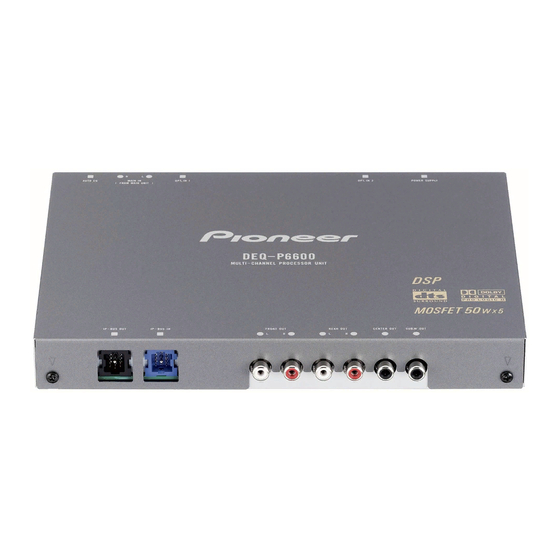
DEQ-P6600
DEQ-P7650
Manufactured under license from Dolby Laboratories. "Dolby", "Pro Logic", and the double-D symbol
are trademarks of Dolby Laboratories.
"DTS" and "DTS Digital Surround" are registered trademarks of Digital Theater Systems, Inc.
This product cannot be operated independently. Combining DVH-P5000MP/UC etc for performing a
check of operation.
For details, refer to "Important symbols for good services".
PIONEER CORPORATION
PIONEER ELECTRONICS (USA) INC. P.O. Box 1760, Long Beach, CA 90801-1760, U.S.A.
PIONEER EUROPE NV Haven 1087, Keetberglaan 1, 9120 Melsele, Belgium
PIONEER ELECTRONICS ASIACENTRE PTE. LTD. 253 Alexandra Road, #04-01, Singapore 159936
PIONEER CORPORATION 2004
/EW
/ES
4-1, Meguro 1-chome, Meguro-ku, Tokyo 153-8654, Japan
DEQ-P8000/UC
K-ZZA. APR. 2004 printed in Japan
ORDER NO.
CRT3263
/UC
Advertisement
Table of Contents

Related Manuals for Pioneer DEQ-P800/UC


Summary of Contents for Pioneer DEQ-P800/UC
- Page 1 PIONEER CORPORATION 4-1, Meguro 1-chome, Meguro-ku, Tokyo 153-8654, Japan PIONEER ELECTRONICS (USA) INC. P.O. Box 1760, Long Beach, CA 90801-1760, U.S.A. PIONEER EUROPE NV Haven 1087, Keetberglaan 1, 9120 Melsele, Belgium PIONEER ELECTRONICS ASIACENTRE PTE. LTD. 253 Alexandra Road, #04-01, Singapore 159936 PIONEER CORPORATION 2004 K-ZZA.
-
Page 2: Safety Information
SAFETY INFORMATION CAUTION This service manual is intended for qualified service technicians; it is not meant for the casual do-it-yourselfer. Qualified technicians have the necessary test equipment and tools, and have been trained to properly and safely repair complex products such as those covered by this manual. Improperly performed repairs can adversely affect the safety and reliability of the product and may void the warranty. -
Page 3: Table Of Contents
CONTENTS SAFETY INFORMATION............................2 1. SPECIFICATIONS .............................4 2. EXPLODED VIEWS AND PARTS LIST......................8 2.1 PACKING ..............................8 2.2 EXTERIOR ...............................10 3. BLOCK DIAGRAM AND SCHEMATIC DIAGRAM ..................12 3.1 BLOCK DIAGRAM............................12 3.2 OVERALL CONNECTION DIAGRAM(GUIDE PAGE) ................14 4. PCB CONNECTION DIAGRAM ........................20 4.1 AUDIO CONTROL UNIT...........................20 5. -
Page 4: Specifications
1. SPECIFICATIONS DEQ-P8000/UC... - Page 5 DEQ-P8000/UC...
- Page 6 DEQ-P8000/UC...
- Page 7 DEQ-P8000/UC...
-
Page 8: Exploded Views And Parts List
2. EXPLODED VIEWS AND PARTS LIST OTES : • Parts marked by " * " are generally unavailable because they are not in our Master Spare Parts List. • Screw adjacent to mark on the product are used for disassembly. •... - Page 9 (1) PACKING SECTION PARTS LIST Mark No. Description Part No. Mark No. Description Part No. Cord Assy CDE5880 Angle CNB2351 Cord CDE6775 Fastener CNM3728 Cord Assy CDE7531 Microphone Assy CPM1066 Screw Assy CEA2440 Filter See contrast table(2) Screw BNC40P120FZK Optical Cable Connection Box See contrast table(2) Polyethylene Bag CEG1158...
-
Page 10: Exterior
2.2 EXTERIOR DEQ-P8000/UC... - Page 11 (1) EXTERIOR SECTION PARTS LIST Mark No. Description Part No. Mark No. Description Part No. Screw BMZ30P040FTC Connector(CN961) CKS3124 Screw BSZ30P060FZK Connector(CN172) CKS3125 ••••• Pin Jack(CN122) CKS3144 Cord Assy CDE7531 Pin Jack(CN751) CKS3144 Fuse(10A) CEK1136 Pin Jack(CN752) CKS3144 Cord Assy CDE7719 Connector(CN201) CKS3410...
-
Page 12: Block Diagram And Schematic Diagram
3. BLOCK DIAGRAM AND SCHEMATIC DIAGRAM 3.1 BLOCK DIAGRAM AUDIO CONTROL UNIT IC361/IC3 IC302 NJM4580M PCM1604Y-2 IC361 CN101 DAC_FL Q101 SDOB0 LPF FO DATA1 OUT1 2SC2412K DDIN0 FL & R OPT1IN DDIN0 SDOB1 DATA2 DAC_FR IC101 OUT2 SDOB2 DATA3 IC381 CN102 DAC_RL TC7WH08FU... - Page 13 IC351 IC361/IC381 TC9164AF NJM4580MD IC451/IC452 FMG12 MIX_L IC801/IC802 GAIN SELECTOR EVOL L CH AND CENTER CN801 NJM4580MD Q501-503 PAL007A IC361 IC501 ADD FOR LPF FOR CDL+ SPKR1L FLIN L-COM1 L-S1 PML011A FL & RL LEFT L-S2 CDR+ SPKR1R L-S3 NAVI+ SPKR2R FRIN IC381...
-
Page 14: Overall Connection Diagram(Guide Page)
3.2 OVERALL CONNECTION DIAGRAM(GUIDE PAGE) Note: When ordering service parts, be sure to refer to " EXPLODED VIEWS AND PARTS LIST" or "ELECTRICAL PARTS LIST". Large size SCH diagram OPTICAL SIGNAL LINE ANALOG SIGNAL LINE Guide page Detailed page ANALOG: +8dBs YSSCLK SYSPW... - Page 15 The > mark found on some component parts indicates the importance of the safety factor of the part. : The power supply is shown with the marked box. Therefore, when replacing, be sure to use parts of identical designation. AUDIO CONTROL UNIT PRE OUT >...
- Page 16 DEQ-P8000/UC...
- Page 17 DEQ-P8000/UC...
- Page 18 DEQ-P8000/UC...
- Page 19 DEQ-P8000/UC...
-
Page 20: Pcb Connection Diagram
4. PCB CONNECTION DIAGRAM 4.1 AUDIO CONTROL UNIT NOTE FOR PCB DIAGRAMS 1.The parts mounted on this PCB include all necessary parts for several destination. AUDIO CONTROL UNIT For further information for respective destinations, be sure to check with the schematic dia- gram. - Page 21 SIDE A CORD ASSY IC,Q OPT2 IN FRONT PREOUT REAR PREOUT CENTER & LFE DEQ-P8000/UC...
- Page 22 AUDIO CONTROL UNIT IC,Q DEQ-P8000/UC...
- Page 23 SIDE B DEQ-P8000/UC...
-
Page 24: Electrical Parts List
5. ELECTRICAL PARTS LIST NOTE: Parts whose parts numbers are omitted are subject to being not supplied. • The part numbers shown below indicate chip components. • Chip Resistor RS1/_S___J,RS1/__S___J Chip Capacitor (except for CQS..) CKS.., CCS.., CSZS..Circuit Symbol and No. Part No. - Page 25 Circuit Symbol and No. Part No. Circuit Symbol and No. Part No. D 754 Diode 1SS355 L 756 Inductor CTF1473 D 801 Diode SC016-2 L 757 Inductor CTF1473 D 802 Diode SC016-2 L 801 Choke Coil 600µH CTH1275 D 803 Diode SC016-2 L 901...
- Page 26 Circuit Symbol and No. Part No. Circuit Symbol and No. Part No. R 198 RS1/16S104J R 366 RS1/16S3901D R 199 RS1/16S222J R 367 RS1/16S822J R 201 RS1/16S101J R 368 RS1/16S822J R 202 RS1/16S101J R 369 RS1/16S1502D R 204 RS1/16S472J R 370 RS1/16S1502D R 221 RS1/16S0R0J...
- Page 27 Circuit Symbol and No. Part No. Circuit Symbol and No. Part No. R 477 RS1/16S4701D R 632 RAB4C101J R 478 RS1/16S4701D R 633 RAB4C471J R 479 RS1/16S0R0J R 634 RS1/16S473J R 480 RS1/16S0R0J R 635 RS1/16S473J R 481 RS1/16S0R0J R 636 RS1/16S471J R 482 RS1/16S0R0J...
- Page 28 Circuit Symbol and No. Part No. Circuit Symbol and No. Part No. CAPACITORS R 763 RS1/16S390J R 764 RS1/16S390J R 765 RS1/16S390J C 101 CKSRYB104K25 R 766 RS1/16S390J C 102 CKSRYB104K25 R 767 RS1/16S390J C 103 CKSRYB104K25 C 104 CCSRCH470J50 R 768 RS1/16S390J C 105...
- Page 29 Circuit Symbol and No. Part No. Circuit Symbol and No. Part No. C 255 CKSRYB104K25 C 401 CKSRYB472K50 C 256 CCSRCH100D50 C 402 CKSRYB104K25 C 257 CKSRYB104K25 C 403 CKSRYB102K50 C 258 CKSRYB104K25 C 404 CKSRYB473K50 C 259 CCSRCH100D50 C 405 CCSRCH470J50 C 260 CCSRCH471J50...
- Page 30 Circuit Symbol and No. Part No. Circuit Symbol and No. Part No. C 706 CKSRYB105K10 C 908 CEHVW330M16 C 707 CEVW100M16 C 909 CEHVW330M16 C 708 CEVW100M16 C 910 CKSYB475K10 C 709 CKSRYB105K10 C 911 CKSYB225K16 C 710 CCSRCH470J50 C 912 CEVW330M16 C 711 CCSRCH470J50...
-
Page 31: Adjustment
6. ADJUSTMENT There is no information to be shown in this chapter. DEQ-P8000/UC... -
Page 32: General Information
7. GENERAL INFORMATION 7.1 DIAGNOSIS 7.1.1 DISASSEMBLY Removing the Case (Fig.1) Case Remove the four screws and then remove the Case. Fig.1 Removing the Audio Control Unit (Fig.2) Remove the screw. Remove the two screws. Straighten the tabs at four locations indicated. -
Page 33: Connector Function Description
7.1.2 CONNECTOR FUNCTION DESCRIPTION IP-BUS OUTPUT IP-BUS INPUT FRONT REAR SUBWOOFER CENTER OUTPUT OUTPUT OUTPUT OUTPUT 1. BUS+ 7. BUSL+ 1. BUS+ 7. BUSL+ 2. GND 8. ASENB 2. GND 8. ASENB 3. GND 9. BUSR+ 3. GND 9. BUSR+ 4. - Page 34 7.2 IC HA12240FP * XC25BS5118MR BIAS DRIVER Counter OUTPUT (CURRENT) RECEIVER OUTPUT Fuse 11bit Pll Select (XN) * TC7WB383FK IC's marked by * are MOS type. Be careful in handling them because they are very liable to be damaged by electrostatic induction. * AN8015SH Triangular wave OSC...
- Page 35 - Pin Functions(AK7730VT) Pin No. Pin Name Function and Operation EESEL Control Mode select pin (Pull down) JX0/SDIN4A External conditional jump pin / DSP serial data input pin (Pull down) 3, 4 SDIN3, 2/JX1, 2 DSP serial data input pin / External condition jump pin (Pull down) SDIN1 DSP serial data input pin (Pull down) CKS1...
- Page 36 * YSS932-S TESTXI TESTXO RAMA11 VDD2 RAMA10 RAMA9 RAMA3 TESTMS RAMA4 TESTXEN RAMA2 IPORT0 RAMA5 IPORT1 RAMA1 IPORT2 RAMA6 IPORT3 RAMA0 IPORT4 RAMA7 DDIN0 RAMA8 DDIN1 VDD1 DDIN2 DDIN3 RASN RAMOEN RAMWEN AVDD CASN DIRPCO RAMD15 DIRPRO RAMD14 AVSS RAMD13 TESTBRK RAMD12 TESTR1...
- Page 37 Block diagram IPORT5-7 VMOD BSMOD DDINSEL UMOD CMOD D B L D I R P C O D I R M C K DIR Clock (25MHz) D I R B C K DIRO Interface D I R W C K D I R S D O S D B C K I 0 S D I A...
- Page 38 * PCM1604Y-2 36 35 34 33 32 31 30 29 28 27 26 25 SCKI ADND3 SCKO ADND4 LRCK TEST ADND5 DGND ADND6 DATA1 CAP1 DATA2 CAP2 DATA3 ZEROA 10 11 12 Block diagram LRCK Serial DATA1(V 1,2) input I/F Output Amp DATA2(V 3,4)
- Page 39 - Pin Functions(PD5967A) Pin No. Pin Name Format Function and Operation YSSCLK YSS932 : Communication CLK evolstb2, 1 DOLPHIN2, 1 : Strobe EVOLTX DOLPHIN : Communication data output DOLPHIN : Communication CLK output EVOLCLK CNVSS Not used reset Microcomputer hard reset input XOUT System clock output System clock input (10MHz)
- Page 40 Pin No. Pin Name Format Function and Operation DSPPW DSP : Power supply output ysslock YSS : PLL lock detection terminal DACRX DAC : Communication data input AK7730 : DRDY detection terminal AKDRDY AKRDY AK7730 : RDY detection terminal AKMCK switch (fs32K) H : 32kHz L : Others 32KSW AKCKS1 AK7730 : Master clock selection pin 1...
-
Page 41: Operational Flow Chart
7.3 OPERATIONAL FLOW CHART Power ON VCC=5V Pin 13/78 bsens Pin 15 bsens=L asens Pin 16 asens=L MUTERQ←H Pin 51 IPPW←H Pin 21 Source ON SYSPW←H Pin 60 DSPPW←H Pin 61 Completes power-on operation. DEQ-P8000/UC... -
Page 42: Cleaning
7.4 CLEANING Before shipping out the product, be sure to clean the following portions by using the prescribed cleaning tools: Portions to be cleaned Cleaning tools Fans Cleaning paper : GED-008 DEQ-P8000/UC... -
Page 43: Operations
8. OPERATIONS - CONNECTION DIAGRAM(UC) This product Noise filter When you connect a power amp (sold separately), be sure to use the blue/white 40cm lead of this unit. If you use the blue/white (1 ft. 3-3/4 in.) lead of the head unit, it causes noises. Blue/white Noise filter To system control terminal of the power... - Page 44 System remote control Blue/white To system control terminal of the power amp or Auto-antenna relay control terminal (max. 300 mA 12 V DC). 40cm When you connect a power amp (sold (1 ft. 3-3/4 in.) separately), be sure to use the blue/white lead of this unit.
- Page 45 DEQ-P8000/UC...
- Page 46 - Jigs List Name Jig No. Remarks Cleaning paper GED-008 Cleaning fans DEQ-P8000/UC...