Table of Contents
Advertisement
Quick Links
SAFETY PRECAUTION FOR SERVICE MANUAL ........................................................................................................... 2
IMPORTANT SERVICE NOTES (FOR U.K. ONLY) .......................................................................................................... 3
SPECIFICATIONS ............................................................................................................................................................. 3
NAMES OF PARTS ........................................................................................................................................................... 4
OPERATION MANUAL ...................................................................................................................................................... 5
DISASSEMBLY .................................................................................................................................................................. 6
REMOVING AND REINSTALLING THE MAIN PARTS ..................................................................................................... 8
ADJUSTMENT ................................................................................................................................................................. 10
BLOCK DIAGRAM ........................................................................................................................................................... 12
SCHEMATIC DIAGRAM / WIRING SIDE OF P.W.BOARD ............................................................................................. 18
NOTES ON SCHEMATIC DIAGRAM .............................................................................................................................. 41
TYPES OF TRANSISTOR AND DIODE .......................................................................................................................... 41
FUNCTION TABLE OF IC ................................................................................................................................................ 42
WIRING OF PRIMARILY SUPPLY LEADS (FOR U.K. ONLY) ........................................................................................ 66
PARTS GUIDE/EXPLODED VIEW/PACKING METHOD (FOR U. K. ONLY)
SERVICE MANUAL
MODEL
CONTENTS
SHARP CORPORATION
- 1 -
DX-SX1H
• In the interests of user-safety the set should be restored to its
original condition and only parts identical to those specified be
used.
This document has been published to be used
for after sales service only.
The contents are subject to change without notice.
DX-SX1H
No. S6053DXSX1H//
SACD PLAYER
Page
Advertisement
Table of Contents

Related Manuals for Sharp DX-SX1H

Summary of Contents for Sharp DX-SX1H
-
Page 1: Table Of Contents
DX-SX1H SERVICE MANUAL No. S6053DXSX1H// SACD PLAYER DX-SX1H MODEL • In the interests of user-safety the set should be restored to its original condition and only parts identical to those specified be used. CONTENTS Page SAFETY PRECAUTION FOR SERVICE MANUAL ......................2 IMPORTANT SERVICE NOTES (FOR U.K. -
Page 2: Safety Precaution For Service Manual
DX-SX1H (Except for U.K.) SAFETY PRECAUTION FOR SERVICE MANUAL Precaution to be taken when replacing and servicing the Laser Pickup. The AEL (Accessible Emission Level) of Laser Power Output for this model is specified to be lower than Class I Requirements. -
Page 3: Important Service Notes (For U.k. Only)
DX-SX1H IMPORTANT SERVICE NOTES (FOR U.K. ONLY) Before returning the unit to the customer after completion of a WITHSTANDING repair or adjustment it is necessary for the following withstand VOLTAGE TESTER voltage test to be applied to ensure the unit is safe for the PROBE customer to use. -
Page 4: Names Of Parts
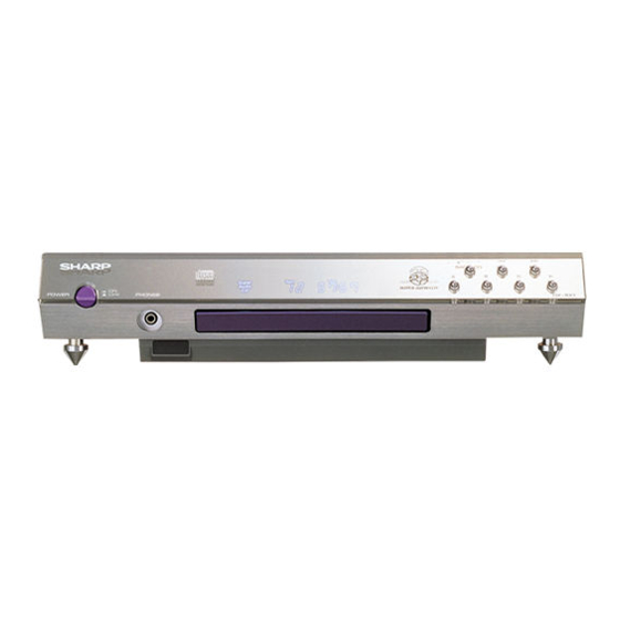
DX-SX1H NAMES OF PARTS – 4 –... -
Page 5: Operation Manual
DX-SX1H OPERATION MANUAL – 5 –... -
Page 6: Disassembly
DX-SX1H DISASSEMBLY Caution on Disassembly Follow the below-mentioned notes when disassembling (D1)x1 (D1)x2 ø2.6x6mm the unit and reassembling it, to keep it safe and ensure ø2.6x8mm excellent performance: 1. Take compact disc out of the unit. (D1)x1 2. Be sure to remove the power supply plug from the wall ø2.6x6mm... - Page 7 DX-SX1H (H1)x4 ø2.6x6mm Display PWB Top Plate (F1)x2 ø2x5mm (H1)x2 (H1)x1 ø2.6x6mm ø2.6x6mm (F1)x5 ø2.6x8mm Tray Ass'y Figure 7-1 (G1)x4 ø3x6mm (G1)x1 ø1.7x3mm CD Servo PWB (H1)x2 ø2x5mm Tray Sensor (G3)x1 (G3)x1 (G2)x2 Pickup Sensor PWB (G1)x2 (G2)x1 ø2x5mm Mode Switch...
-
Page 8: Removing And Reinstalling The Main Parts
DX-SX1H REMOVING AND REINSTALLING THE MAIN PARTS SACD MECHANISM SECTION Lift Cover Perform steps 1, 4, 7 and 8 of the disassembly method to remove the SACD mechanism. How to remove the loading motor (See Fig. 8-1.) Loading 1. Remove the lift lever. - Page 9 DX-SX1H Adjusting the tension of the timing belt Loading Gear Remove the gear unit and connect the ammeter to the DC Motor Unit power as shown in Fig. 9-1. Connector Ampere Meter 3.5V DC Power Figure 9-1 (A1) x1 If measurement of the loading motor current is possible, move ø1.7x2mm...
-
Page 10: Adjustment
DX-SX1H ADJUSTMENT TEST MODE Description of the test mode 1. How to enter the test mode In the no disc mode and the tray eject mode, press the SACD/CD button and the track down button more than two seconds. Display: F 0 _ _ 0 0 0 0 0 2. - Page 11 DX-SX1H 6. Laser test mode Enter the laser test mode from the dynamic test mode. Display: 3 1 _ 0 0 0 0 0 CD laser lit up (Press the STOP button in the step Display: 3 1 1 0 0 0 0 0...
-
Page 12: Block Diagram
DX-SX1H CD APC CNP501 Q504 SACD Q503 a_IN a_OUT P1AI b_OUT P1BI c_IN c_OUT P1CI d_IN d_OUT P1DI e_IN e_OUT P1FP f_IN f_OUT P1FN IC501 IC502 P1TP TA1244FN IX1517GE P1TN I/V CONVERTER P2AI RF SIGNAL AMP. P2BI PROCESSOR P2CI S/DUAL... - Page 13 DX-SX1H IC605 TC7WU04FU 54MHz TO IC901 3-CIRCUIT INVERTER 24MHz X602 54MHz IC604 TC7W74FU 32 24 1/2 DIVIDING STDA H1,0 H1,0 STCK Buff RFIN IC601 HCEN HCEN AD8052AR Vref IC602 HDRD HDRD DUAL Vref OPE AMP. IX1474GE HDWT HDWT HINT HINT...
- Page 14 DX-SX1H XTAL FL801 KEY1 20MHz KEY2 EXTAL S/E_CS S/E_CK S/E_DA JOG1 UART_RXD JOG2 UART_CTL XMSLA IC801 MSDATI SYSTEM MSCK MICROCOMPUTER RFRP RFRP IX1478GE MSDATO SRV_AD SRV_AD XMSREDY EMPH EMPH ECC_CS SBSY SBSY ECCINT RFLT RFLT SMUTE SBCS SBCS BUCK BUCK...
- Page 15 DX-SX1H IC903 16Mbit SDRAM IX2840AF 13 , 16 5 , 24 6 , 7 , 22 , 23 KEY1 KEY2 E_CS E_CK 51 , 52 , 55 63 E_DA A2~A10 D7~D0 MSLA XMSLAT PCLK DATI WRFD MSCK DATA MSCK MSDATI...
- Page 16 DX-SX1H IC328 TC7WU04U X301 3-CIRCUIT INVERTER 33.8688MHz to TC9461 73PIN MCK IC305 IX2838AF IC301 CDDAT LINE AMP. IC303 CDCLK SM6451AV CD DATA PCM1716E CDFRM VOLUME from TC9461 CD D/A CONTROL RELAY CONVERTER SWITCHING Q305 RELAY DVD L IC326 SWITCHING IX2838AF SACD LINE AMP.
- Page 17 DX-SX1H IC308 NJM4580M HEADPHONES HEADPHONES IC301 AMP. MUTE FL201 SM6451AV Q307 JAK201 FL DISPLAY Q309 VOLUME HEADPHONES IC309 CONTROL IX2838AF LINE AMP. RELAY VAR.OUT SWITCHING IC201 SOC302 Q310 XLF201 LINE OUTPUT MN12510F 4.000MHz FL DRIVER FIX OUT IC310 IX2838AF LINE AMP.
-
Page 18: Schematic Diagram / Wiring Side Of P.w.board
DX-SX1H 0.7V 4.3V Q302 DZ301 R392 DTA114 YK UDZ2.0B SWITCHING 4.7K VOLUME R393 R399 C410 C409 4.7K 4.7K CONTROL R343 C336 10/16 R479 330P 4.4V 4.12V R379 (VOLDT) RSTN 1.8K 4.1V (VOLCK) ADRS1 C333 1.8K IC328 10/16 R380 4.1V ADRS2... - Page 19 DX-SX1H MAIN PWB-A1 R392 CD SIGNAL 4.7K IC308 R399 NJM4580M 4.7K Q307,Q309 : HEADPHONES MUTE HEADPHONES AMP. R379 (VOLDT) C479 1.8K 0.001 C376 Q307 Q309 4.1V (VOLCK) DTC323 TK 47P(CH) DTC323 TK 1.8K R386 4.3V CNP305 R380 C368 4.1V (VOLCS) 4.3V...
- Page 20 DX-SX1H FL201 FL DISPLAY -25.8V -25.8V C202 -25.7V -25.7V 0.047 D201 (FILAMENT(+)) DAP202K D203 Q203 -28.5V DAP202K 2SA1037 KR C201 R226 R201 2.2K R210 4.9V 4.6V R212 -25.3V 4.7K 5.0V (AT5V) (AT-30V) D_GND FILAMENT(-) AT-30V -31.5V FILAMENT(+) -25.1V KEY2 5.0V...
- Page 21 DX-SX1H C209 0.047 Q203 -28.5V 2SA1037 KR Q204 R226 DTC124 EK 2.2K 4.9V 0.4V 4.6V R212 4.7K 5.0V R225 R217 (S1) (S2) R218 SW206 SW207 -28.5V NEXT OPEN/CLOSE -25.7V (S3) (G7) R219 -28.5V -25.7V (S4) (G8) R220 -22.4V -28.4V (S5)
- Page 22 DX-SX1H CNP101 RP10 D108 C128 Posis 13.9V R192 C151 D4SBS6 A_GND 3900/25 A_GND C136 R193 C152 -14.1V P19 10 - G -14.1V 3900/25 13.3V CNS101B C137 (12.9V) TO MAIN PWB D_GND RP103 C114 2.2 Posistor 6800/25 C129 P-IN (2.5V) RP102...
- Page 23 DX-SX1H CNS105 CNP105 RP101 D108 Posistor D4SBS6 C136 -14.1V C137 RP102 Posistor -25.1V D109 D4SB60L -25.1V F102 T2A L 250V -25.1V C133 -10V C134 F103 T2A L 250V IC102 BP5220 DC/DC CONVERTER 2 3 4 5 6 7 8 9 0V 0V 13.3V...
- Page 24 DX-SX1H WARF WADT WACK RSTO_1 FL801 ECCCS 20MHz R839 ECCINT R842 L801 47µH C802 C805 R852 0.01 47/6.3 4.7K SDCK SOSO C806 3.5V (EXCS) C814 SVAL EXP-CS 0.01 SERR (U-CT) R821 AVCC UART-CTL 3.3K (S/E_CK) 4.5V VREF SUB/EEP CLK (KEY1) (U-RX) 0.3V...
- Page 25 DX-SX1H SACD PWB-C(1/2) R861 C822 0.001 CD SIGNAL R862 R923 R915 R918 3.3K 3.3K D3.3V(2) R911 D3.3V(2)L901 C907 R925 16Mbit SDRAM R936 IC903 C910 IX2840 AF 0.01 C908 C911 0.01 47/6.3 R908 1.5V 1.7V 4.1V C904 3.5V 3.5V XSRQ WRFD 0.01...
- Page 26 DX-SX1H P27 P28 SACD PWB-C(2/2) CD SIGNAL Q501 R521 R542 2SA1037 KR R527 C523 C529 R519 47/10 47/10 L501 4.7K C527 SEL_1 SEL_2 GAIN 10µH C516 0.01 PICKUP UNIT -2dB R518 D505 0.01 R563 2.2K +2dB R529 DAP202K R545 FLEXIBLE...
- Page 27 DX-SX1H C672 R605 10P(CH) R542 C626 0.01 R590 R612 R527 8.2K C523 C529 4 .9V 47/10 47/10 L501 R589 C527 10µH C538 0.01 D505 R563 R529 DAP202K R545 R580 C548 C561 2.2V 0.01 47/6.3 3.3M C559 R614 R610 2.0V 47/6.3 2.0V...
- Page 28 DX-SX1H C672 R605 10P(CH) WARF WADT WACK C626 RSTO_1 0.01 33MHZ R612 4 .9V (D15) ECCCS 27MHz 18µs 18µs ECCINT C561 2.2V C648 47/6.3 0.01 C559 R614 R610 47/6.3 2.4V TP506 TP507 C656 A_GND 2.1V 1 12 100/6.3 TP508 C562 TP509 4.8V...
- Page 29 DX-SX1H R190 B C E R191 Q121 C104 CNS102A CNP102 C108 P35 11 - E C110 CNP904 TO SACD PWB C105 CNS102B COLOR TABLE BROWN RD(R) C120 ORANGE RP106 YELLOW GREEN C116 C121 R178 BLUE R181 IC103 VIOLET R177 C109...
- Page 30 DX-SX1H P35 7 - H TO SACD PWB CNP902 P39 12 - E CNS309B 1 2 3 4 TO HEADPHONES PWB 5 6 7 8 9 10 11 CNS202B 1 2 3 4 5 6 7 8 9 10 11...
- Page 31 DX-SX1H MAIN PWB-A1 (TOP VIEW) R366 X301 D301 C440 IC305 C379 R365 L307 REY301 C406 C473 6 7 8 9 10 Q305 R331 C439 R436 L305 C317 R363 C368 R322 20 25 Q304 L306 R435 C405 IC328 C411 C444 IC304...
- Page 32 DX-SX1H CK90 R391 CK89 CK142 CK156 CK158 C305 R357 CK147 R305 CK91 R350 R344 C340 C342 CK181 TP306 R323 CK146 R326 C313 CK101 C460 CK149 CK102 CK108 CK97 CK126 CK107 TP309 R477 CK73 CK104 CK136 C334 CK138 CK71 CK179 CK139...
- Page 33 DX-SX1H MAIN PWB-A1(BOTTOM VIEW) R391 R473 CK92 CK87 R429 CK36 CK121 CK29 R471 CK27 C376 CK30 CK150 R470 CK165 CK152 C337 CK86 CK170 CK136 C334 CK138 C336 CK139 R376 CK26 R384 CK144 CK143 CK168 C356 R377 R480 R479 CK172 CK84...
- Page 34 DX-SX1H P40 3 - G TO PICKUP IN SENSOR PWB CNS51B TO SPINDLE MOTOR P40 5 - D TP505 CK128 C544 P40 3 - C CK127 CNS502 CNS52B TO TRAY CK41 SENSOR PWB IC501 C567 CK34 TP511 C515 CK131 CK42...
- Page 35 DX-SX1H TO SPINDLE MOTOR P40 5 - D C918 CK40 C557 CK46 R591 CNS502 R940 R585 CK47 C530 R584 R592 CK41 P40 5 - H CNP502 R520 CK34 TO LOADING TP511 C515 CK38 CK42 MOTOR IC505 TP502 C514 C539 CK39...
- Page 36 DX-SX1H R583 R648 R582 IC507 C545 C806 R821 R832 C802 R852 R822 C808 R810 R811 R812 R813 R814 R815 R816 R848 R802 C809 R804 R855 C819 R828 R910 Q801 R836 R831 5 10 15 20 R834 R865 R859 R860 R838...
- Page 37 DX-SX1H Q501 Q502 R542 R519 R541 C516 Q506 C556 Q504 R545 C919 Q503 C555 R513 R527 R506 C531 R512 Q505 C532 R505 R563 R590 R593 R580 R528 C506 R933 R934 R629 C633 P31 11 - G CNS301B C634 C638 TO MAIN PWB...
- Page 38 DX-SX1H DISPLAY PWB-A2 (TOP VIEW) FL201 IC201 R217 R222 D201 R225 R219 D203 Q203 R212 Q204 DISPLAY PWB-A2 (BOTTOM VIEW) CK57 CK21 CK56 CK29 CK28 CK25 CK41 CK30 CK46 CK44 : Through-hole where the top and bottom patterns are connected.
- Page 39 DX-SX1H HEADPHONES PWB-A3 (TOP VIEW) CNP201 C204 SW202 PREV JAK201 HEADPHONES XLF201 C211 TERMINAL C206 SW206 SW201 NEXT SACD/ CNP202 1 2 3 SW207 SW203 SW204 CNP203 SW205 OPEN/CLOSE PLAY PAUSE STOP CNS202A CNS201C COLOR TABLE 1 2 3 1 2 3 4...
- Page 40 DX-SX1H P34 2 - D PICKUP (314) TO SACD PWB CNP505 CNS53B 3 2 1 3 2 1 CNS53A 3 2 1 CNP53 SW52 SW51 STOP PLAY CNS501 P34 2 - C MODE SWITCH MODE SWITCH TO SACD PWB PWB-D2...
-
Page 41: Notes On Schematic Diagram
DX-SX1H NOTES ON SCHEMATIC DIAGRAM • Resistor: • The indicated voltage in each section is the one measured To differentiate the units of resistors, such symbol as K and by Digital Multimeter between such a section and the chas- M are used: the symbol K means 1000 ohm and the symbol sis with no signal given. -
Page 42: Function Table Of Ic
DX-SX1H FUNCTION TABLE OF IC IC201 VHiMN12510F-1: FL Driver (MN12510F) Pin No. Terminal Name Name Input/Output Function VDD: +5V ± 0.5V Power supply terminal Input VSS: 0V FLP driver power supply Input VPP: VDD - 35V Applies voltage to pull-down resistor SEG0-7 and DGT0-7. - Page 43 DX-SX1H IC102 VHiBP5220++-1: DC/DC Converter (BP5220) Terminal Function Name Feedback terminal VOUT Output terminal DRIVING CIRCUIT ON, OFF terminal N.C. Not used POWER CONTROL CIRCUIT CIRCUIT Output voltage fine adjustment terminal N.C. Not used N.C. N.C. — Cut pin N.C.
- Page 44 DX-SX1H IC302 VHiDSD1700E-1: DSD Converter (DSD1700E) Pin No. Terminal Name Input/Output Function DGND — Digital ground — Digital power supply, +5V Input Reset control input, active at LOW PHASE Input Select data phase (LOW: through, HIGH: inversion) DGND AGND —...
- Page 45 DX-SX1H IC303 VHiPCM1716E-1: CD D/A Converter (PCM1716E) Pin No. Terminal Name Input/Output Function LRCK Input LRCK clock input (fs) DATA Input Data input Input Data bit clock input CLKO Output System clock, buffered output Input Connection of crystal transmitter or external clock input...
- Page 46 DX-SX1H IC502 RH-iX1517GEZZ: RF Signal Processor (IX1517GE) (1/2) Terminal DC Remarks Pin No. Terminal Name Input/Output Function Voltage (TYP.) — GND terminal — P2TP Input TE+ input (CD) P2TN Input TE- input (CD) LDO2 Output Drive output — MDI2 Input Monitor output —...
- Page 47 DX-SX1H IC502 RH-iX1517GEZZ: RF Signal Processor (IX1517GE) (2/2) Terminal DC Remarks Pin No. Terminal Name Input/Output Function Voltage (TYP.) P1FP Input FE+ input LDP1 Input APC polarity 1 — Positive polarity when connecting to Vcc P1DI Input D input (DVD)
- Page 48 DX-SX1H IC503 VHiTB6504F+-1: Stepping Motor Driver (TB6504F) Pin No. Terminal Name Function Clock signal input 2, 3 M1, M2 Excitation mode set terminal REF IN Output reference value (VNF) set terminal H: VNF=0.5V, L: VNF=0.25V Monitor output L: Initial condition...
- Page 49 DX-SX1H IC504 RH-iX2842AFZZ: Spindle Motor Driver (IX2842AF) Terminal Terminal Pin No. Function Pin No. Function Name Name Power GND terminal Signal GND terminal Hall element 1 positive input terminal Power terminal Hall element 1 negative input terminal Torque instruction reference input terminal...
- Page 50 DX-SX1H IC506 VHiBA6796FP-1: Loading/Focus/Tracking/Spin/Sled Driver (BA6796FP) Terminal Terminal Function Function Name Name OPOUT Operational amplifier output terminal CH2-OUT- CH2 negative output terminal CH4-IN CH4 input terminal CH2-OUT+ CH2 positive output terminal CH4-IN' CH4 gain adjustment input terminal CH1-OUT- CH1 negative output terminal...
- Page 51 DX-SX1H IC602 RH-iX1474GEZZ: SACD Data Processor (IX1474GE) (1/2) Terminal Pin No. Remarks Input/Output Function Name DPCKI Input Signal processing reference clock input 0.5 - 3.3Vpp, feedback resistor built in. DVDD3 — Digital power supply (3.3V) For logic cell SVCKI Input Servo reference clock input (Oscillation circuit input terminal) 3.3V-I/F feedback resistor built in...
- Page 52 DX-SX1H IC602 RH-iX1474GEZZ: SACD Data Processor (IX1474GE) (2/2) Terminal Pin No. Remarks Input/Output Function Name DVDD3 — Digital power supply (3.3V) For logic cell 85-88 SD3-SD0 Output MPEG data output SERR Output MEPG data reliability flag (Data error = "L")
- Page 53 DX-SX1H IC606 RH-iX1473GEZZ: Digital Servo (IX1473GE) (1/3) Terminal Pin No. Remarks Input/Output Function Name — Digital ground terminal Output Bit clock (1.4122 MHz) output terminal AOUT Output Audio data output terminal DOUT Output Digital-out output terminal MBOV Output When buffer memory over signal output terminal is over: "H"...
- Page 54 DX-SX1H IC606 RH-iX1473GEZZ: Digital Servo (IX1473GE) (2/3) Terminal Pin No. Remarks Input/Output Function Name Output Tracking equalizer output terminal VREF — Analog reference power terminal RFGC Output Outputs 3-pole PWM signal of RF amplitude adjusting signal output terminal. (PWM carrier = 88.2 kHz)
- Page 55 DX-SX1H IC606 RH-iX1473GEZZ: Digital Servo (IX1473GE) (3/3) Terminal Pin No. Remarks Input/Output Function Name — Digital + power terminal — Digital ground terminal BUCK Input Clock input terminal for microcomputer interface Schmitt input /CCE Input Chip enable signal input terminal for microcomputer interface Schmitt input "L": BUS0 to 3 are active.
- Page 56 DX-SX1H IC801 RH-iX1478GEZZ: System Microcomputer (IX1478GE) PORT D PORT E /IRQ7 /IRQ6 /IRQ5 /IRQ4 EXTAL XTAL STBY H8S/2000 CPU WDTOVF INTERRUPT CONTROLLER /ø DMAC ROM * /HWR /LWR /LCAS/WAIT/BFEQO /BACK /BREQ /CS0 /CS1 /CS2 /CS3 /SCK1 /SCK0 /CAS /RxD1 /CS7/IRQ3...
- Page 57 DX-SX1H IC802 RH-iX1535GEZZ: Input/Output Expander (IX1535GE) (1/2) Pin No. Terminal Name Input/Output Function — Power supply +3.3V HADR0-HADR2 Input CPU address bus Input CPU chip select Input CPU write signal Input CPU read signal 8-15 HDAT0-HDAT7 Input/Output CPU data bus —...
- Page 58 DX-SX1H IC802 RH-iX1535GEZZ: Input/Output Expander (IX1535GE) (2/2) Pin No. Terminal Name Input/Output Function MODE Input Mode switching terminal. Fix at "L". BUFCO Input/Output Buffer output C TEST Input Test terminal. Fixed at "L". BUFCI Input Buffer input C. Not used.
- Page 59 DX-SX1H IC804 RH-iX2839AFZZ: 1Mbit SRAM (IX2839AF) Pin No. Terminal Name Function Not used Address input Address input Address input 5-12 A7-A0 Address input 13-15 I/O1-I/O3 Data input/output Ground 17-21 I/O4-I/O8 Data input/output Chip enable input Address input Output enable input...
- Page 60 DX-SX1H IC805 RH-iX1539GEZZ: Flash ROM (IX1539GE) (1/2) Pin No. Terminal Name Input/Output Function A15-A13 Input Block select addresses: Select 1/32 erase block. These addresses are latched during data entry, erase and lock block. A12-A8 Input Word select addresses: Select one word in 1.6k byte block.
- Page 61 DX-SX1H IC805 RH-iX1539GEZZ: Flash ROM (IX1539GE) (2/2) Pin No. Terminal Name Input/Output Function Input/Output Lower byte data input/output: Data and command input during cycle of writing command user interface. Memory array, identifier, and status data output when reading various data.
- Page 62 DX-SX1H IC901 VHiCXD2751Q-1: SACD Playback Signal Processor (CXD2751Q) (1/2) Pin No. Terminal Name Input/Output Function XSRQ Output Output terminal for data request to be input in the front end processor. XSHD Input Input terminal for header flag to be output from the front end processor.
- Page 63 DX-SX1H IC901 VHiCXD2751Q-1: SACD Playback Signal Processor (CXD2751Q) (2/2) Pin No. Terminal Name Input/Output Function BCKA Input/Output Shift clock input/output terminal for DSD data output. Input/output according to setting. DSAL Output Lch-DSD data output terminal. Phase modulation output according to setting.
- Page 64 DX-SX1H IC902 VHiADC08351-1: A/D Converter (ADC08351) Pin No. Terminal Name Function CMOS/TTL compatible digital input terminal. When this terminal is set to Low, digital output of ADC08351 becomes enable. When this terminal is set to High, digital output changes to the high-impedance condition.
- Page 65 DX-SX1H IC903 RH-iX2840AFZZ: 16Mbit SDRAM (IX2840AF) Pin No. Terminal Name Function 28 pin plastic TSOP 28 pin plastic SOJ (Type K) Power supply (3.3V) DQ1-DQ4 Data input/output Write enable Row address strobe Not used A10R Address input 10-13 A0-A3 Address input Power supply (3.3V)
-
Page 66: Wiring Of Primarily Supply Leads (For U.k. Only)
DX-SX1H WIRING OF PRIMARILY SUPPLY LEADS (FOR U.K. ONLY) If any one of the bands shown in Fig. 66 is removed for some reason, be sure replace it to the original position and same appearance as before. Figure 66 – 66 –... - Page 67 “HOW TO ORDER REPLACEMENT PARTS” To have your order filled promptly and correctly, please furnish the For U.S.A. only following information. Contact your nearest SHARP Parts Distributor to order. 1. MODEL NUMBER 2. REF. No. 3. PART NO. 4. DESCRIPTION For location of SHARP Parts Distributor, Please call Toll-Free;...
- Page 68 DX-SX1H PRICE PRICE PARTS CODE DESCRIPTION PARTS CODE DESCRIPTION RANK RANK INTEGRATED CIRCUITS D109 VHDD4SB60L+-1 AG Rectifier Diode,D4SB60L D201 VHDDAP202K/-1 AB Silicon,DAP202K D203 VHDDAP202K/-1 AB Silicon,DAP202K IC101 VHIKIA7805P-1 AF Voltage Regulator,KIA7805P D301~303 VHDDAP202K/-1 AB Silicon,DAP202K IC102 VHIBP5220++-1 AT DC/DC Converter,BP5220...
- Page 69 DX-SX1H PRICE PRICE PARTS CODE DESCRIPTION PARTS CODE DESCRIPTION RANK RANK AA 0.1 µF,50V AA 0.1 µF,25V C201 VCKYTV1HF104Z C459,460 VCKYTV1EB104K AA 0.047 µF,50V C202 VCKYTV1HB473K C461,462 VCKYTV1HB221K AA 220 pF,50V AA 0.01 µF,50V AC 100 µF,16V,Electrolytic C203 VCKYTV1HB103K C463,464 RC-EZ0476GEZZ AD 10 µF,16V,Electrolytic...
- Page 70 DX-SX1H PRICE PRICE PARTS CODE DESCRIPTION PARTS CODE DESCRIPTION RANK RANK C623 VCKYCY1HB471K AA 470 pF,50V R224 VRS-TV2AB471J AA 470 ohms,1/10W AA 0.01 µF,25V C625,626 VCKYCY1EB103K R225 VRS-TV2AB333J AA 33 kohms,1/10W AD 100 µF,6.3V,Electrolytic C627 VCEAPW0JW107M J R226 VRS-TV2AB222J AA 2.2 kohms,1/10W AA 0.01 µF,25V...
- Page 71 DX-SX1H PRICE PRICE PARTS CODE DESCRIPTION PARTS CODE DESCRIPTION RANK RANK R457,458 VRS-TV2AB470J AA 47 ohms,1/10W R614 VRS-CY1JB330J AA 33 ohms,1/16W R459~461 VRS-TV2AB563J AA 56 kohms,1/10W R615,616 VRS-CY1JB471J AA 470 ohms,1/16W R462 VRS-TV2AB680J AA 68 ohms,1/10W R618 VRS-CY1JB102J AA 1 kohm,1/16W...
- Page 72 DX-SX1H PRICE PRICE DESCRIPTION PARTS CODE PARTS CODE DESCRIPTION RANK RANK OTHER CIRCUITRY PARTS LHLDM1065AFZZ AY Stabilizer LHLDZ1785AFM1 AH Tray Guide Bearing Ass’y,A LHLDZ1786AFZZ AG Tray Guide Bearing,B BI101A/B QCNWN6834AFZZ J AG Connector Ass’y,2/2Pin BI301A/B QCNWN6825AFZZ J AN Connector Ass’y,7/7Pin...
- Page 73 DX-SX1H PRICE PRICE PARTS CODE DESCRIPTION PARTS CODE DESCRIPTION RANK RANK PSPAZ0585AFZZ AD Insulate Bush PSPAZ0638AFZZ AF Insulate Spacer TLABP0465AFZZ Label,Fuse LX-BZ1013AFFO AC Screw,ø3×8mm LX-HZ0082AFZZ AA Screw,ø4×8mm LX-HZ0241AFFO AE Screw,ø4×7mm XBBSD20P05000 AA Screw,ø2×5mm XBBSD20P10000 AA Screw,ø2×10mm XBPSD26P05J00 AA Screw,ø2.6×5mm XBPSD30P08J00 AA Screw,ø3×8mm...
- Page 74 DX-SX1H 717x3 718x2 705x2 701x2 701x2 312x2 711x4 717x2 309x2 PWB-D3 713x2 718x2 M703 711x2 711x2 719x2 SW52 SW51 PWB-D1 PWB-D2 711x2 711x4 Figure 7 SACD MECHANISM EXPLODED VIEW – 7 –...
- Page 75 DX-SX1H 603x5 622x4 SACD MECHANISM UNIT 232x2 607x2 PWB-B2 608x2 620x2 PWB-C 619x3 227x3 619x2 609x4 620x2 616x2 619x5 PWB-A3 615x2 604x2 607x2 619x3 PWB-A2 611x5 SOC1 FL201 619x3 248x3 604x2 604x2 620x2 616x3 605x2 604x5 621x4 224x2 619x2 228x2...
- Page 76 SSAKA0226AFZZ 19. Core RCoRF0015CFZZ 10. Sheet, Unit SSAKH0330AFZZ © COPYRIGHT 2000 BY SHARP CORPORATION SHARP CORPORATION ALL RIGHTS RESERVED. Communication Systems Group Quality & Reliability Control Center No part of this publication may be reproduced, Higashihiroshima, Hiroshima 739-0192, Japan stored in a retrieval system, or transmitted in...