Table of Contents
Advertisement
Quick Links
ELECTRONICS
This Service Manual is a property of Samsung Electronics Co.,Ltd.
Any unauthorized use of Manual can be punished under applicable
international and/or domestic law.
© Samsung Electronics Co., Ltd. JUL. 2006
Printed in Korea
MF82-00282A
DIGITAL CABLE RECEIVER
BASIC : DSB-S300G
Application Models
: DCB-P850R, DCB-P850RS
Application Areas
:
SERVICE
DIGITAL CABLE RECEIVER
DCB-P850Z, DCB-P850ZS
DCB-P853Z, DCB-P853ZS
BAS, XEN, XEE
Manual
Merit & Character regarding Product
ΠDual Recording
´ Picture in Picture (2 Tuners)
ˇ Timeshift
¨ High speed USB 2.0 Host
ˆ SRS TrusurroundXT for Virtual
Surround Sound
Ø Built-in 160GB HDD (Up to 80 hours Recording)
∏ Electronic Progarm Guide (EPG)
" Digital Audio Output (SPDIF, Optical)
' 1 Smart Card
Advertisement
Table of Contents

Related Manuals for Samsung DSB-S300G


Summary of Contents for Samsung DSB-S300G
- Page 1 ” Digital Audio Output (SPDIF, Optical) ’ 1 Smart Card © Samsung Electronics Co., Ltd. JUL. 2006 This Service Manual is a property of Samsung Electronics Co.,Ltd. Printed in Korea Any unauthorized use of Manual can be punished under applicable international and/or domestic law.
-
Page 2: Table Of Contents
CONTENTS 1. Precautions 1-1 ~ 1-4 1-1 Safety Precaution (1-1) 1-2 Servicing Precautions (1-3) 1-3 ESD Precautions (1-4) 2. Product Specification 2-1 ~ 2-4 2-1 Product Specification (2-1) 2-2 Chassis Product Specification (2-2) 2-3 Option Product Specification (2-4) 3. Software Update 3-1 ~ 3-2 3-1 DCB-P850R(S),DCB-P850Z(S) Software Update (3-1) - Page 3 CONTENTS 11. Schematic Diagrams 11-1 ~ 11-14 11-1 S.M.P.S (S.M.P.S PCB) (11-2) 11-2 Tuner (Main PCB) (11-3) 11-3 DDR Interface (Main PCB) (11-4) 11-4 Flash Scart (Main PCB) (11-5) 11-5 TS Interface,USB2.0,JATG (Main PCB) (11-6) 11-6 ATA Interface (Main PCB) (11-7) 11-7 AV Interface (Main PCB) (11-8)
- Page 4 Metal Part cal return path to the chassis. Any current measured must not exceed 0.5mA. Reverse the instrument power cord plug in the out- ohmmeter let and repeat the test. See Fig. 1-1. Fig. 1-2 Insulation Resistance Test Samsung Electronics...
- Page 5 (5) antenna wiring. Always inspect in all areas tinuously and new instructions are issued whenev- for pinched, out-of-place, or frayed wiring, Do not er appropriate. change spacing between a component and the printed-circuit board. Check the AC power cord for damage. Samsung Electronics...
-
Page 6: Precautions 1-1
Components identi- fied by shading, by( ) or by ( ) in the circuit dia- gram are important for safety or for the characteris- tics of the unit. Always replace them with the exact replacement components. Samsung Electronics... -
Page 7: Esd Precautions
(6) Do not remove a replacement ESD device from its protective package until immediately before your are ready to install it.(Most replacement ESD devices are packaged with leads electrically short- ed together by conductive foam, aluminum foil or comparable conductive materials). Samsung Electronics... -
Page 8: Product Specification 2-1
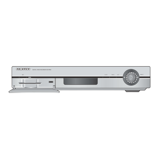
32, 44.1, 48kHz Scart(TV) Video(CVBS/RGB), Audio L/R Scart(VCR) Video(CVBS), Audio L/R A/V Output RCA Jack Video(CVBS), Audio L/R Digital Audio Output Optical Size (W x D x H): 381 x 267 x 60 mm Phisical Specification Weight (Net) 3.1 Kg Samsung Electronics... -
Page 9: Chassis Product Specification
L/R CH : RCA SCART VCR Input Display Module 10Digits VFD Module Power LED Indicator O(Power on:Green,Standby:Red) O(Power on: None,Standby:Red) IR LED Display AC3 LED Display Type 36-Key Standard 47-Key Standard Color Silver Black Battery Type AAA 2EA AAA 2EA Samsung Electronics... - Page 10 Component Video Cable A/V RCA Cable RF Cable Modem Cable Input Voltage AC 100-240V~,50/60 Hz AC 230V~,50/60 Hz Power Consumption Max.25W Max.30W Size 270 x 200 x 45 mm 381 x 267 x 60 mm Weight 1.2Kg 3.1Kg Samsung Electronics...
-
Page 11: Option Product Specification
Remote Model Standard MF59-00287A Control of DCB-P850Z/XEE Model Standard Batteries for 4301-000115 of DCB-P850Z/XEE Remote Control S.N.A Model Standard MF68-00409A User’s Manual of DCB-P850Z/XEE Model Standard RF Cable AC39-00017A of DCB-P850Z/XEE Model Standard SCART Cable AH39-00043B of DCB-P850Z/XEE Samsung Electronics... -
Page 12: Software Update 3-1
To scan particular channel, select a mode between Auto and Manual. In the manual mode, you can select the channel and PID. To start the software upgrade, press the OK button. Caution : When the receiver is transferring, you must keep a thing intact until transfer is ended. Samsung Electronics... - Page 13 Software Update MEMO Samsung Electronics...
-
Page 14: Disassembly And Reassembly 4-1
DCB-P850RS/P850ZS/P853ZS (3 X 8 S) DCB-P850R/P850Z/P853Z (3 X 10 B) ˇ 3 SCREWS DCB-P850RS/P850ZS/P853ZS (3 X 8 S) DCB-P850R/P850Z/P853Z (3 X 10 B) ¨ 3 SCREWS (3 X 8 S) ˆ TOP CABINET Fig. 4-1 Top Cabinet removal Samsung Electronics... - Page 15 Disassembly and Reassembly 4-1-2 Ass’y Hard Disk Removal 1) Remove 4 Screws Œ. 2) Remove Ass’y Hard Disk ´. Œ 4 SCREWS (2.8 X 4 S) ´ ASS’Y HARD DISK Fig. 4-2 Ass’y Hard Disk Removal Samsung Electronics...
- Page 16 4-1-3 Main PCB, S.M.P.S PCB Removal 1) Remove 8 Screws Œ. 2) Remove Main PCB ´, S.M.P.S PCB ˇ. Œ 8 SCREWS (3 X 6 S) ˇ S.M.P.S PCB ´ MAIN PCB Fig. 4-3 Main PCB, S.M.P.S PCB Removal Samsung Electronics...
- Page 17 Disassembly and Reassembly 4-1-4 Ass’y Front Removal 1) Remove 4 Hooks Œ, ´, ˇ. 2) Remove Ass’y Front ¨. ´ 1 HOOK ¨ ASS’Y FRONT Œ 1 HOOK ˇ 2 HOOKS Fig. 4-4 Ass’y Front Removal Samsung Electronics...
- Page 18 1) Remove 3 Screws Œ, ´. 2) Remove Fan ˇ. 3) Remove Chassis Rear ¨. Œ 2 SCREWS (5 X 14 S) ¨ CHASSIS REAR ˇ FAN Œ 1 SCREW (3 X 8 S) Fig. 4-5 Chassis Rear, Fan Removal Samsung Electronics...
- Page 19 Disassembly and Reassembly MEMO Samsung Electronics...
-
Page 20: Troubleshooting
If the controller is Check the voltage operating unstably or no of Vcc for SMPS operation,change the PQIZ1 controller Check the Check the shorting at connection at several main power several main power Connect between SMPS and Main Power Samsung Electronics... - Page 21 Change for same spec tuner. from ˇ20pin to ¨28pin. Clock & Data OK? ˇ Clock : 20Pin (TS_CLK) Check serial registers' Correct resistors of condition of TS & control pins. location(R105~R116). No problem ? ¨ Data : 28pin (TS_DATA) Check Decoder "U302". Samsung Electronics...
- Page 22 Check ´ CVBS at Video filter(C756,L708, 4pin of U701? C763,C773,R736,C715) Check ˇ CVBS at Check Failure mode of U701 ´ CVBS at 4Pin of U701 36pin of U701? Check Failure mode of J703 ˇ CVBS at 36Pin of U701 Samsung Electronics...
- Page 23 Check ˇ CVBS at Check Failure mode of U701 44pin of U701 ´ CVBS at 4pin of U701 Check CVBS at Check R806,R812, ,C809 19pin of Scart Connector ˇ CVBS at 44pin of U701, Check Failure mode of J801 SCART Connector Samsung Electronics...
- Page 24 ¨ Pin 42,15 Check Open or Short at the circuit Check R/G/B signal at R : R805,R811,C808 Pin ¨15,ˆ11,Ø7 G : R804,R810,C807 of SCART Jack B : R803,R809,C806 ˆ Pin 40,11 Check RGB-Jack Connection (STB°ÍTV). Ø Pin 38,7 Samsung Electronics...
- Page 25 Troubleshooting SPDIF Output Missing (Optical) Check +5V Check +5V Drive at Pin2 of J702 ΠDigital Audio signal at R714 Check Failure mode Check ΠDigital Audio U302(STi5100) signal at R714 Check J702 Optical Jack Failure mode Samsung Electronics...
- Page 26 Pin28,27 of U701 Failure mode. ˇ Analog Audio output at Pin28,27 of U701 Check ¨ Audio signal at Check U1001 Failure mode and application circuit L706, L705 Check Failure mode of J703(RCA Connector) ¨ Audio signal at L706, L705 Samsung Electronics...
- Page 27 Pin33,32 of U701 Failure mode. Check Open or Shot ˇ Analog Audio output at Check ¨ Analog Audio Circuit at C801,R801,C804, Pin33,32 of U701 Signal at L801,L802 L801,R807 Check Failure mode of J801(SCART Connector) ¨ Analog Audio Signal at L801,L802 Samsung Electronics...
- Page 28 ´ DM(pin3), DP(pin4), J1202 and Flat cale Connection VBUS(pin2) of J1301 (Front Board) Check Open or Short at J1302(USB connector) on Front Board Œ Signal at pin 1, 3 of U502 ´ DM(pin3), DP(pin4), VBUS(pin2) of J1301 (Front Board) Samsung Electronics...
- Page 29 = Master ´ U603 Pin11 : ATA Address Check Open or Short at Check the Data Signal at U601,U602,U603,U604,U605 Œ U603,´ U604, and Their Circuit ˇ U605 ˇ U604/U605 Pin2 : ATA Data Check Failure mode of HDD 5-10 Samsung Electronics...
-
Page 30: Exploded View And Parts List
6-1 Ass’y Chassis - - - - - - - - - - - - - - - - - - - - - - - - - - - - - - - - - - - - - - 6-2 Samsung Electronics... - Page 31 Exploded View and Parts List 6-1 Ass’y Chassis W260 W260 W001 W336 W001 C527 VS105 C015 C904 P295 W260 W001 W271 W268 W275 P025 P030 P001 P003 S.N.A : Service Not Available A001 P005 W009 C022 C001 Samsung Electronics...
- Page 32 P295 MF97-00373A ASSY BRACKET-HDD;SECC T0.8,DTB-P8 VS105 AK39-00024A WIRE HARNESS;DVD-H40,UL2678#30 80 W001 6003-000275 SCREW-TAPTITE;BH,+,B,M3,L10 DCB-P850R/XEN 6003-000275 SCREW-TAPTITE;BH,+,B,M3,L10 DCB-P850Z/XEE W009 6003-000276 SCREW-TAPTITE;BH,+,-,B,M3,L10,ZPC W260 6003-001547 SCREW-TAPTITE;BH,+,-,B-TITE,M3,L8 DCB-P850RS/XEN W268 6003-000254 SCREW-TAPTITE;BH,+,-,S,M3,L6,ZPC( W271 6009-001411 SCREW-SPECIAL;TH,+,-,M5,L14,NI PL W275 6003-001561 SCREW-TAPTITE;BH,+,-,B,M3,L6,ZPC( W336 6001-000742 SCREW-INCH MACH;PH,+,UNC6-32,L4.2 Samsung Electronics...
- Page 33 Exploded View and Parts List MEMO Samsung Electronics...
-
Page 34: Electrical Parts List
C1211 2401-000240 C-AL;100uF,20%,10V,GP,TP,5x11,5 C704 2401-002144 C-AL;47uF,20%,16V,GP,TP,5x11,5 C705 2203-005065 C-CER,CHIP;1000nF,+80-20%,10V,Y5 C129 2401-000240 C-AL;100uF,20%,10V,GP,TP,5x11,5 C706 2401-002144 C-AL;47uF,20%,16V,GP,TP,5x11,5 C157 2203-005148 C-CER,CHIP;100nF,10%,16V,X7R,160 C158 2203-005148 C-CER,CHIP;100nF,10%,16V,X7R,160 C708 2203-000646 C-CER,CHIP;0.024NF,5%,50V,C0G,TP C159 2203-005148 C-CER,CHIP;100nF,10%,16V,X7R,160 C709 2203-000646 C-CER,CHIP;0.024NF,5%,50V,C0G,TP Samsung Electronics This Document can not be used without Samsung’s authorization... - Page 35 2401-000414 C-AL;10uF,20%,16V,GP,TP,4x7,5 C938 2203-005148 C-CER,CHIP;100nF,10%,16V,X7R,160 C939 2203-005148 C-CER,CHIP;100nF,10%,16V,X7R,160 C776 2203-005148 C-CER,CHIP;100nF,10%,16V,X7R,160 C940 2203-005148 C-CER,CHIP;100nF,10%,16V,X7R,160 C777 2203-000236 C-CER,CHIP;0.1nF,5%,50V,C0G,1608 C941 2203-005148 C-CER,CHIP;100nF,10%,16V,X7R,160 C801 2401-002144 C-AL;47uF,20%,16V,GP,TP,5x11,5 C942 2401-002144 C-AL;47uF,20%,16V,GP,TP,5x11,5 C803 2401-002144 C-AL;47uF,20%,16V,GP,TP,5x11,5 Samsung Electronics This Document can not be used without Samsung’s authorization...
- Page 36 3301-001495 BEAD-SMD;120ohm,2012,2500mA,TP,1 R113 2007-000113 R-CHIP;33ohm,5%,1/10W,TP,1608 L703 3301-001495 BEAD-SMD;120ohm,2012,2500mA,TP,1 L705 2703-000229 INDUCTOR-SMD;6.8UH,20%,2012 R114 2007-000113 R-CHIP;33ohm,5%,1/10W,TP,1608 R115 2007-000113 R-CHIP;33ohm,5%,1/10W,TP,1608 L706 2703-000229 INDUCTOR-SMD;6.8UH,20%,2012 R116 2007-000113 R-CHIP;33ohm,5%,1/10W,TP,1608 L707 2703-000125 INDUCTOR-SMD;10uH,10%,2012 R118 2007-000122 R-CHIP;1.2Kohm,5%,1/10W,TP,1608 Samsung Electronics This Document can not be used without Samsung’s authorization...
- Page 37 2007-000450 R-CHIP;180ohm,5%,1/10W,TP,1608 R617 2007-000113 R-CHIP;33ohm,5%,1/10W,TP,1608 R326 2007-000074 R-CHIP;100ohm,5%,1/10W,TP,1608 R618 2007-000113 R-CHIP;33ohm,5%,1/10W,TP,1608 R327 2007-000450 R-CHIP;180ohm,5%,1/10W,TP,1608 R620 2007-000090 R-CHIP;10Kohm,5%,1/10W,TP,1608 R328 2007-000074 R-CHIP;100ohm,5%,1/10W,TP,1608 R329 2007-000113 R-CHIP;33ohm,5%,1/10W,TP,1608 R621 2007-000090 R-CHIP;10Kohm,5%,1/10W,TP,1608 R622 2007-000113 R-CHIP;33ohm,5%,1/10W,TP,1608 Samsung Electronics This Document can not be used without Samsung’s authorization...
- Page 38 U602 0801-002403 IC-CMOS LOGIC;74LCX08,AND GATE,T R817 2007-000077 R-CHIP;470ohm,5%,1/10W,TP,1608 U603 0802-001007 IC-CMOS LOGIC;74LCX244,BUFFER/LI R818 2007-000077 R-CHIP;470ohm,5%,1/10W,TP,1608 U604 0801-002095 IC-CMOS LOGIC;74LCX245,TRANSCEIV R819 2007-000106 R-CHIP;220Kohm,5%,1/10W,TP,1608 U605 0801-002095 IC-CMOS LOGIC;74LCX245,TRANSCEIV R820 2007-000106 R-CHIP;220Kohm,5%,1/10W,TP,1608 Samsung Electronics This Document can not be used without Samsung’s authorization...
- Page 39 C-FILM,LEAD-PEF;1000nF,5%,100V,T PQTZ1 MF26-00161A TRANS SWITCHING;EER3534,DTB-P850 PFCZ1 2301-000402 C-FILM,LEAD-PEF;1nF,5%,50V,TP,5x PFID1 AC14-12006D IC;KA431Z,TO-92,TAPING PRCU1 2401-003842 C-AL;100uF,20%,450V,WT,BK,25.4X2 PSCX1 2305-001029 C-FILM,LEAD-PEF;10nF,10%,630V,TP PFRD1 2001-000429 R-CARBON;1KOHM,5%,1/8W,AA,TP,1.8 PSCZ2 2201-000129 C-CERAMIC,DISC;0.1nF,10%,1000V,Y PFRD2 2001-000527 R-CARBON;22OHM,5%,1/8W,AA,TP,1.8 PSDZ1 0402-000012 DIODE-RECTIFIER;UF4007,1KV,1A,DO Samsung Electronics This Document can not be used without Samsung’s authorization...
- Page 40 J1301 3708-000170 CONNECTOR-FPC/FFC/PIC;15P,1.25MM U1301 1003-001039 IC-VFD;UPD16311GC-AB6,QFP,52P,55 J1302 3722-002313 JACK-USB;4P/1C,AU30U,BLK,STRAIGH VF1301 MD07-00001A VFD DISPLAY;DTB-P850F,HNV-12SM97 3811-000389 WIRE-NO SHEATH CU;SPCW,300V,52.4 JP10 3811-000389 WIRE-NO SHEATH CU;SPCW,300V,52.4 VF1301 MF61-00105A HOLDER-VFD;DTB-P850F,ABS 94HB,-, AC99-40105Q ASSY PCB-MAIN VCR,c;SLV-D990PB,Z Samsung Electronics This Document can not be used without Samsung’s authorization...
- Page 41 W009 6003-000276 SCREW-TAPTITE;BH,+,-,B,M3,L10,ZP W260 6003-001547 SCREW-TAPTITE;BH,+,-,B-TITE,M3,L W260 6003-001547 SCREW-TAPTITE;BH,+,-,B-TITE,M3,L W268 6003-000254 SCREW-TAPTITE;BH,+,-,S,M3,L6,ZPC W271 6009-001411 SCREW-SPECIAL;TH,+,-,M5,L14,NI P W275 6003-001561 SCREW-TAPTITE;BH,+,-,B,M3,L6,ZPC W307 6001-001868 SCREW-MACHINE;PWH,+,-,M2.6,L4,ZP W336 6001-000742 SCREW-INCH MACH;PH,+,UNC6-32,L4. AH39-00043B CABLE-SCART;-,-,21P,1200MM,-,-,P AC39-00017A CABLE-ETC-RF(PAL);-,MALE/FEMALE, Samsung Electronics This Document can not be used without Samsung’s authorization...
-
Page 42: Block Diagrams
8-3 U301 (DDRSDRAM) Block Diagram - - - - - - - - - - - - - - - - - - - - - - - - - - - - This Document can not be used without Samsung’s authorization. -
Page 43: All Block Diagram
Block Diagrams 8-1 All Block Diagram U301 U302 U401 This Document can not be used without Samsung’s authorization. Samsung Electronics... - Page 44 2x I/F MAFE I/F Transport Steam decoder SmCard Tx/Rx amd SiLabs Central merger DisEqC Audio UARTs SSCs DACs TS0IN TS2IN TS1IN Analog audio ser/par TS2OUT par/D1 out L/R 1394OUT This Document can not be used without Samsung’s authorization. Samsung Electronics...
-
Page 45: Ddrsdram Block Diagram
I/O GATING Input DQ0- DM Mask Logic Regiser DQ15, Mask LDM, Write 512(x32) FIFO & Data Column A0-A12, Column-address Drivers Decoder BA0, BA1 Conuter/Latch LDQS, COL0 UDQS COL0 CK,CK This Document can not be used without Samsung’s authorization. Samsung Electronics... -
Page 46: Wiring Diagram
9. Wiring Diagram Samsung Electronics... - Page 47 Wiring Diagram MEMO Samsung Electronics...
-
Page 48: Pcb Diagrams
10-3 S.M.P.S PCB - - - - - - - - - - - - - - - - - - - - - - - - - - - - - - - - - - - - - - - - - - - 10-6 10-1 Samsung Electronics... -
Page 49: Main Pcb
PCB Diagrams 10-1 Main PCB COMPONENT SIDE U301 B-3 U1001 C-1 U701 E-1 Sti5100 U301 U701 U1001 10-2 Samsung Electronics... - Page 50 ˇ CVBS at Pin 4 of U701 ” U603 Pin1 : ATA Select ¨ CVBS at Pin 36,44 of U701 ’ U603 Pin11 : ATA Address ¨ Ø ˆ∏ ˆ Pin 40 of U701 ˝ U604/U605 Pin2 : ATA Data Samsung Electronics 10-3...
- Page 51 PCB Diagrams CONDUCTOR SIDE 10-4 Samsung Electronics...
-
Page 52: Front Pcb
PCB Diagrams 10-2 Front PCB COMPONENT SIDE CONDUCTOR SIDE Samsung Electronics 10-5... -
Page 53: Pcb
PCB Diagrams 10-3 S.M.P.S PCB COMPONENT SIDE 10-6 Samsung Electronics... - Page 54 PCB Diagrams CONDUCTOR SIDE Samsung Electronics 10-7...
- Page 55 PCB Diagrams MEMO 10-8 Samsung Electronics...
- Page 56 11-12 Front (Front PCB) - - - - - - - - - - - - - - - - - - - - - - - - - - - - - - - - - - - - - - - 11-13 This Document can not be used without Samsung’s authorization. 11-1...
-
Page 57: Schematic Diagrams
Schematic Diagrams 11-1 S.M.P.S (S.M.P.S PCB) This Document can not be used without Samsung’s authorization. Samsung Electronics 11-2... -
Page 58: Schematic Diagrams 11-1
Œ I2C_CLK ´ I2C_Data ˇ TS CLK ¨ TS DATA ◆ These are the waveforms of DCB-P850R/P850RS/P850Z/P850ZS Caution) There can be some differences (Voltage, Frequency, stc.) among cameras. This Document can not be used without Samsung’s authorization. 11-3 Samsung Electronics... -
Page 59: Ddr Interface (Main Pcb)
Schematic Diagrams 11-3 DDR Interface (Main PCB) Sheet 2 of 10 This Document can not be used without Samsung’s authorization. Samsung Electronics 11-4... -
Page 60: Flash Interface (Main Pcb)
Schematic Diagrams 11-4 Flash Interface (Main PCB) Sheet 3 of 10 This Document can not be used without Samsung’s authorization. 11-5 Samsung Electronics... -
Page 61: Ts Interface,Usb2.0,Jatg (Main Pcb)
11-5 TS Interface,USB2.0,JATG (Main PCB) Sheet 4 of 10 Œ USB ◆ These are the waveforms of DCB-P850R/P850RS/P850Z/P850ZS Caution) There can be some differences (Voltage, Frequency, stc.) among cameras. This Document can not be used without Samsung’s authorization. Samsung Electronics 11-6... -
Page 62: Ata Iterface (Main Pcb)
Sheet 5 of 10 Œ ATA Address ´ ATA Select ˇ ATA Data ◆ These are the waveforms of DCB-P850R/P850RS/P850Z/P850ZS Caution) There can be some differences (Voltage, Frequency, stc.) among cameras. This Document can not be used without Samsung’s authorization. 11-7 Samsung Electronics... -
Page 63: Av Switch (Main Pcb)
’ R_1 out ¨ CVBS_1 ˝ CBVS_4 ˆ Audio L, R ◆ These are the waveforms of DCB-P850R/P850RS/P850Z/P850ZS Caution) There can be some differences (Voltage, Frequency, stc.) among cameras. This Document can not be used without Samsung’s authorization. Samsung Electronics 11-8... -
Page 64: Av Output (Scart) (Main Pcb)
Schematic Diagrams 11-8 AV Output(SCART) (Main PCB) Sheet 7 of 10 Video Audio This Document can not be used without Samsung’s authorization. 11-9 Samsung Electronics... -
Page 65: Sst5100 Vcc&Gnd (Main Pcb)
120ohm_2.5A(2012 120ohm_2.5A(2012) 3V3D VDDDE 1V2D C942 C916 C914 C943 C944 C945 C946 C947 C948 C949 C950 C951 C952 C953 C954 C955 C938 C939 C940 C941 47uF/16V DGND AGND This Document can not be used without Samsung’s authorization. Samsung Electronics 11-10... -
Page 66: S-Card,Power (Main Pcb)
Schematic Diagrams 11-10 S-Card, Power (Main PCB) Sheet 9 of 10 This Document can not be used without Samsung’s authorization. 11-11 Samsung Electronics... -
Page 67: Reset,Rs232,Eeprom (Main Pcb)
Schematic Diagrams 11-11 Reset,RS232,EEPROM (Main PCB) Sheet 10 of 10 This Document can not be used without Samsung’s authorization. Samsung Electronics 11-12... -
Page 68: Front (Front Pcb) (Main Pcb)
Schematic Diagrams 11-12 Front (Front PCB) This Document can not be used without Samsung’s authorization. 11-13 Samsung Electronics... - Page 69 Schematic Diagrams MEMO Samsung Electronics 11-14...
-
Page 70: Operating Instructions 12-1
12. Operating Instructions Samsung Electronics 12-1... - Page 71 Operating Instructions Samsung Electronics 12-2...
- Page 72 Operating Instructions Samsung Electronics 12-3...
- Page 73 Operating Instructions Samsung Electronics 12-4...
- Page 74 Operating Instructions Samsung Electronics 12-5...
- Page 75 Operating Instructions Samsung Electronics 12-6...
-
Page 76: Circuit Operating Descriptions 13-1
The received RF input signal split two ways by splitter for input of two tuners and RF out at rear panel. To boost the divided RF signal, 5V is supplied. 13-1-2 Block Diagram AN IN Booster Tuner in Splitter RF OUT fig. 13-1 Samsung Electronics 13-1... -
Page 77: Tuner (Tm101, Tm102)
Function of QAM-Demod block makes the MPEG-2 TS (Transport Stream) by QAM demodulation. TS is consists of D at a [ 0: 7] , Sync, Er r or , Val i d and Cl ock signals. Tuner is controlled by I2C. 13-2-2 Block Diagram fig. 13-2 13-2 Samsung Electronics... -
Page 78: Main Processor (U302)
TV out 8K DCache omterface S/PDIF Audio 2x I/F MAFE I/F Transport Steam decoder SmCard Tx/Rx amd SiLabs Central merger DisEqC Audio UARTs SSCs DACs TS0IN TS2IN TS1IN Analog audio ser/par TS2OUT par/D1 out L/R 1394OUT fig. 13-3 Samsung Electronics 13-3... - Page 79 16-bit wide interface. Bus cycle strobe timings can be programmed from 0 to 15 phases for slower peripherals. The FMI output drive of the STi5100 is programmable on a bus-by-bus basis. Support is provided for connection to an ATAPI HDD. 13-4 Samsung Electronics...
- Page 80 An internal multiplexor routes this to the stream merger’s upper port, which has an internal by-pass directly to the PTI. D1 header processing and buffering is performed by the PTI. Transport deMUX and D1 processing may not be performed simultaneously. 1) Block diagram: Transport stream merger inputs and outputs fig. 13-4 Samsung Electronics 13-5...
- Page 81 When the PTI is required to output a transport stream, it can output the entire transport stream or selected packets filtered by PID. A latency counter is provided to ensure packet timing is preserved. Packet substitution can also be performed. 13-6 Samsung Electronics...
- Page 82 • Alpha with pixel (ARGB1555 or ARGB4444, true color mode only). When mixing OSD regions the still picture layer and decoded video are output on the composite outputs (YC and CVBS), component (RGB/YUV) and digital video outputs. The capability for a separate VCR output is also supported. Samsung Electronics 13-7...
- Page 83 (S-VHS(Y/C) + CVBS + RGB) or (S-VHS(Y/C)+ CVBS + YUV) or (Y1 + C1 + CVBS1 +C2 + Y2 + CVBS2). The encoder can operate in master mode or in one of several modes where it locks onto incoming sync signals. 13-8 Samsung Electronics...
- Page 84 The audio decoder outputs IEC958/IEC1937 formatted CD or PCM audio received from the audio decoder. • 1-channel PCM output interface The PCM output interface outputs PCM audio received from the audio decoder. • Integrated 24-bit stereo audio DAC system • Programmable tone generation for dish alignment Samsung Electronics 13-9...
- Page 85 • Fast 2-D unaligned memory-to-memory transfers of graphics and stills, • Real-time stream transfers to and from memory with or without pacing. These channels are suitable for transfers with external peripherals, HDD and for audio and video stream transfers within the STi5100. 13-10 Samsung Electronics...
- Page 86 • DiSEqC. 2.0 control support, interface to STMicroelectronics LNBP21 PSU controller or a discrete external solution, • Interface to SiLabs line side device (DAA), • An interrupt level controller, • A low-power/RTC/watchdog controller, • DCU toolset support, • A JTAG/TAP interface. Samsung Electronics 13-11...
-
Page 87: Memory Interface
If a byte/word program is attempted while VPEN ≤ VPENLK, SR.4 and SR.3 will be set. Successful byte/word programs require that the corresponding block lock-bit be cleared. If a byte/word program is attempted when the corresponding block lock-bit is set, SR.1 and SR.4 will be set. 13-12 Samsung Electronics... - Page 88 If a command other than Write Confirm is written to the device, an “Invalid Command/Sequence” error will be generated and SR.5 and SR.4 will be set. For additional buffer writes, issue another Write to Buffer Setup command and check XSR.7. Samsung Electronics 13-13...
- Page 89 Machine Vdtage Switch 64-Mbit: Sixty-four 128-Mbit: One-hundred Address X-Decoder Latch twenty-eight 128-Kbyte Blccks Address Counter fig. 13-6 2) HDD This saves the video files which are received from broadcasting and MP3&JPEG files from external memory (USB Interface). 13-14 Samsung Electronics...
- Page 90 • 7.8µs Maximum Average Periodic Refresh Interval • 2.5 V (SSTL_2 compatible) I/O • VDDQ = 2.5 V ± 0.2 V • VDD = 2.5 V ± 0.2 V • P-TFBGA-60-11 package • P-TSOPII-66-1 package • RoHS Compliant Products1) Samsung Electronics 13-15...
- Page 91 An auto refresh mode is provided along with a power-saving power-down mode. All inputs are compatible with the JEDEC Standard for SSTL_2. All outputs are SSTL_2, Class II compatible. 13-16 Samsung Electronics...
- Page 92 Circuit Operating Descriptions 3) Block Diagram - 512-Mbit Double-Data-Rate SDRAM Drivers Receivers Read Latch Bank0 Row-Address latch Bank Control Logic &Decoder Row-address MUX Refresh Counter Address Register fig. 13-7 Samsung Electronics 13-17...
-
Page 93: Video Out
The available output signals are Y, C, CVBS, R, G and B which are connected to Video/Audio switching control IC (STV6412) through filter circuit. 13-5-1 Block Diagram – Video out. Y-Fiter CVBS C-Fiter CVBS-Fiter STI5100 STV6412 (Video DAC of (Audio/Audio Main Processor) R-Fiter Switch IC) G-Fiter B-Fiter CVBS fig. 13-8 13-18 Samsung Electronics... -
Page 94: Audio Out
The level of analog audio L and R signals is small, so these signals go to amp IC (BA4560). The audio signal output is connected with audio and video switching IC(STV6412). 13-6-1 Block Diagram – Audio Out SPDIF STV6412 STV6412 (Audio DAC of (Vidio AMP) Main Processor) fig. 13-9 Samsung Electronics 13-19... -
Page 95: Smart Card Interface(Tda8024)
PIO bits to provide the clock, reset, and I/O functions on the card interface. Smartcard interfaces are supported for the STi5100. This interfaces automatically detects and removes power to the smartcard when smartcard removal is detected. 13-7-1 Block Diagram – Smart Card fig. 13-10 13-20 Samsung Electronics... -
Page 96: Usb Interface
STI5100 provides the USB 2.0 Host. This function supports that MP3 and JPEG files save to internal HDD from external USB memory, MP3 Player and DSC. 13-8-1 Block Diagram – USB USBL C6-2P6 STi5100 (USB Interface of Main Processor) VBUS USB_PWR LM3526-H VBUS Controller USB_OVRI fig. 13-11 Samsung Electronics 13-21... - Page 97 Circuit Operating Descriptions MEMO 13-22 Samsung Electronics...
-
Page 98: Reference Information
NTSC signal requires slightly less transmission capacity at 168 Mbps. The situation becomes much more acute, when one realises that high definition TV is just around the corner. A High Definition TV (HDTV) picture requires a raw bandwidth exceeding 1 Gbps (1000 Mbps). Samsung Electronics 14-1... - Page 99 AC-3 is a sound encoding/decoding technology developed in 1987 for movie theaters and means an AC-3 bit stream.AC-3 is used synonymously with Dolby Digital nowadays. 14-2 Samsung Electronics...
- Page 100 In the past, time shifting was done with a video cassette recorder (VCR) and its timer function, in which the VCR tunes into the appropriate station and records the show onto video tape Samsung Electronics 14-3...
-
Page 101: Model Declartion
5. 8 : SD High-end Model 6. 5 : 2005 Generation 7. 0 : Basic 3 : Derivation 8. CAS name 1) R : Irdeto 2) Z : Conax 9. None : Black Color : Silver Color 14-4 Samsung Electronics...