
Related Manuals for Toshiba MD9DN1R


Summary of Contents for Toshiba MD9DN1R
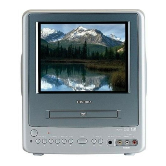
- Page 1 FILE NO. 140-200327 SERVICE MANUAL COLOR TELEVISION/ DVD VIDEO PLAYER MD9DN1R DOCUMENT CREATED IN JAPAN, Jul., 2003...
-
Page 2: Caution
CAUTION THIS DIGITAL VIDEO PLAYER EMPLOYS A LASER SYSTEM. TO ENSURE PROPER USE OF THIS PRODUCT, PLEASE READ THIS SERVICE MANUAL CARE- FULLY AND RETAIN FOR FUTURE REFERENCE. SHOULD THE UNIT REQUIRE MAINTENANCE, CONTACT AN AUTHORIZED SERVICE LOCATION-SEE SERVICE PROCEDURE. USE OF CONTROLS, ADJUSTMENTS OR THE PERFORMANCE OF PROCEDURES OTHER THAN THOSE SPECIFIED HEREIN MAY RESULT IN HAZARDOUS RADIATION EXPOSURE. -
Page 3: How To Order Parts
SERVICING NOTICES ON CHECKING 1. KEEP THE NOTICES 6. AVOID AN X-RAY As for the places which need special attentions, Safety is secured against an X-ray by consider- they are indicated with the labels or seals on the ing about the cathode-ray tube and the high cabinet, chassis and parts. -
Page 4: Important Safeguards
IMPORTANT SAFEGUARDS READ INSTRUCTIONS All the safety and operating instructions should be read before the unit is operated. RETAIN INSTRUCTIONS The safety and operating instructions should be retained for future reference. HEED WARNINGS All warnings on the unit and in the operating instructions should be adhered to. FOLLOW INSTRUCTIONS All operating and use instructions should be followed. - Page 5 IMPORTANT SAFEGUARDS (CONTINUED) DAMAGE REQUIRING SERVICE Unplug this unit from the wall outlet and refer servicing to qualified service personnel under the following conditions: When the power-supply cord or plug is damaged. If liquid has been spilled, or objects have fallen into the unit. If the unit has been exposed to rain or water.
-
Page 6: Disc Removal Method At No Power Supply
DISC REMOVAL METHOD AT NO POWER SUPPLY Remove the Back Cabinet and AV PCB/DVD Block. (Refer to item 1 of the DISASSEMBLY INSTRUCTIONS.) Slide the Rack Loading (White) toward the arrow direction by using a minus driver to release the lock. (Refer to Fig. -
Page 7: Table Of Contents
TABLE OF CONTENTS CAUTION ..........................A1-1 SERVICING NOTICE ON CHECKING ................... A1-2 HOW TO ORDER PARTS ...................... A1-2 IMPORTANT SAFEGUARDS ....................A1-3, A1-4 DISC REMOVAL METHOD AT NO POWER SUPPLY ............A1-5 PARENTAL CONTROL-RATING LEVEL ................A1-5 TRAY LOCK ..........................A1-5 TABLE OF CONTENTS ...................... - Page 8 GENERAL SPECIFICATIONS CRT Size / Visual Size 9 inch / 228.6 mmV System CRT Type Normal Deflection 90 degree Magnetic Field BV/BH +0.45G / 0.18G Color System NTSC Speaker 2 Speaker Position Side Size 3 inch Impedance 8 ohm Sound Output 1.2W + 1.2W 10%(Typical) 0.8W + 0.8W...
- Page 9 GENERAL SPECIFICATIONS Regulation Safety Radiation X-Radiation DHHS Laser DHHS Temperature Operation +5oC ~ +40oC Storage -20oC ~ +60oC Operating Humidity Less than 80% RH On Screen Menu(TV) Display Menu Type Icon Picture Brightness Contrast Color Tint Sharpness Sound Bass Treble Balance TV/CATV Add/Delete...
- Page 10 GENERAL SPECIFICATIONS G-10 On Screen Menu (DVD) Display Menu Type Character Language OSD Language Menu SubTitle Audio Picture TV Screen Size OSD Display On/Off Sound DRC (Dynamic Range Control) dts Decode Output(5.1ch/ 2ch) Surround On/Off Center On/Off Sub Woofer On/Off Parental Password Lock/ Un Lock Rating Level...
- Page 11 GENERAL SPECIFICATIONS G-12 Remote Unit RC-GD Control Glow in Dark Remocon Format Custom Code 71-8E h Power Source Voltage(D.C) UM size x pcs UM-4 x 2 pcs Total Keys 45 Key Keys Power Play Stop Search+ Search- Skip+ Skip- Slow+ Slow- Pause Call...
-
Page 12: Tray Lock
(Dolby Digital) (DTS) Surround (Tru Surround) Screen Saver G-14 Accessories Owner's Manual Language English w/Guarantee Card Buyer Model No. MD9DN1R Remote Control Unit Battery UM size x pcs UM-4 x 2 pcs OEM Brand Rod Antenna Poles Terminal Loop Antenna Terminal... - Page 13 GENERAL SPECIFICATIONS G-15 Interface Switch Front Power (Tact) Channel Up Channel Down Volume Up Volume Down Play Open/Close Skip(>>|) Skip(|<<) Still/Pause Stop Main Power SW Rear Main Power SW Indicator Power Yes (Red) Stand-by On Timer Terminals Front Video Input RCA x 1 Audio Input RCA x 2(Stereo)
-
Page 14: Disassembly Instructions
DISASSEMBLY INSTRUCTIONS 1-3: TV/DVD BLOCK (Refer to Fig. 1-3) 1. REMOVAL OF MECHANICAL PARTS Remove the 2 screws 1. AND P.C. BOARDS Disconnect the following connectors: 1-1: BACK CABINET (Refer to Fig. 1-1) (CP301, CP302, CP401 and CP403). Remove the 5 screws 1. Remove the TV/DVD Block in the direction of arrow. - Page 15 DISASSEMBLY INSTRUCTIONS 1-5: FRONT TRAY PLATE/TOP SHIELD Pick Up PCB (Refer to Fig. 1-5) Unlock the 2 supports 1. Remove the Front Tray Plate in the direction of arrow (A). Remove the 12 screws 2. Remove the Top Shield in the direction of arrow (B). DVD Deck Make the sort circuit using a soldering.
-
Page 16: Removal Of Dvd Deck Parts
DISASSEMBLY INSTRUCTIONS 2. REMOVAL OF DVD DECK PARTS Main Chassis Ass’y NOTE 1. Do not disassemble the DVD DECK PARTS except listed Rack Loading parts here. Minute adjustments are needed if the disas- semble is done. If the repair is needed except listed parts, replace the DVD MECHA ASS’Y. - Page 17 DISASSEMBLY INSTRUCTIONS NOTE Main Chassis Ass'y When installing the Clamper Magnet, install it with the green face up. When installing the wire of the Lever Switch, install it correctly as Fig. 2-4-B. When installing the Lever Switch, install it correctly as Traverse Holder Fig.
- Page 18 DISASSEMBLY INSTRUCTIONS NOTE 2-9: GEAR (Refer to Fig. 2-9-A) Unlock the support 1. After the assembly of the Rack Feed, check if the Rack Feed 1/2 is moving smoothly. (Refer to Fig. 2-7-B) Remove the Middle Gear 1/2/3, Idler Gear and Feed Gear. In case of the Rack Feed Ass’y installation, install cor- rectly as Fig.
- Page 19 DISASSEMBLY INSTRUCTIONS NOTE In case of the Idler Arm installation, install as the circled section of Fig. 2-10-B. In case of the Idler Arm Spring installation, install as the circled section of Fig. 2-10-C. In case of the Chassis Spring installation, install as the circled section of Fig.
-
Page 20: Removal Of Anode Cap
DISASSEMBLY INSTRUCTIONS 3. After one side is removed, pull in the opposite direction to 3. REMOVAL OF ANODE CAP remove the other. Read the following NOTED items before starting work. NOTE After turning the power off there might still be a potential Take care not to damage the Rubber Cap. -
Page 21: Removal And Installation Of Flat Package Ic
DISASSEMBLY INSTRUCTIONS When IC starts moving back and forth easily after REMOVAL AND INSTALLATION OF FLAT desoldering completely, pickup the corner of the IC using a PACKAGE IC tweezers and remove the IC by moving with the IC desoldering machine. (Refer to Fig. 4-3.) REMOVAL NOTE Put the Masking Tape (cotton tape) around the Flat... - Page 22 DISASSEMBLY INSTRUCTIONS INSTALLATION When bridge-soldering between terminals and/or the soldering amount are not enough, resolder using a Thin-tip Take care of the polarity of new IC and then install the new Soldering Iron. (Refer to Fig. 4-8.) IC fitting on the printed circuit pattern. Then solder each lead on the diagonal positions of IC temporarily.
-
Page 23: Service Mode List
SERVICE MODE LIST This unit provided with the following SERVICE MODES so you can repair, examine and adjust easily. To enter to the SERVICE MODE function, press and hold both buttons simultaneously on the main unit and on the remote control for more than a standard time (second). -
Page 24: When Replacing Eeprom(Memory) Ic
WHEN REPLACING EEPROM (MEMORY) IC If a service repair is undertaken where it has been required to change the MEMORY IC, the following steps should be taken to ensure correct data settings while making reference to TABLE 1. NOTE: No need setting for after INI 1F due to the adjustment value. Table 1 Enter DATA SET mode by setting VOLUME to minimum. -
Page 25: Electrical Adjustments
ELECTRICAL ADJUSTMENTS BEFORE MAKING ELECTRICAL FUNCTION FUNCTION ADJUSTMENTS OSD H COL. AV(CENT.) OSD CONTRAST COL. AV(MAX) Read and perform these adjustments when repairing the CUT OFF COL. AV(MIN) H POSITION TINT AV circuits or replacing electrical parts or PCB assemblies. H BLK L SHARPNESS AV H BLK R... - Page 26 ELECTRICAL ADJUSTMENTS 2-4: WHITE BALANCE 2-8: VERTICAL LINEARITY NOTE: Adjust after performing CUT OFF adjustment. NOTE: Adjust after performing adjustments in section 2-7. After the adjustment of Vertical Linearity, reconfirm Place the set with Aging Test for more than 15 minutes. the Vertical Position and Vertical Size adjustments.
- Page 27 ELECTRICAL ADJUSTMENTS 2-10: OSD HORIZONTAL 2-13: TINT CENTER Receive the color bar pattern. (RF Input) Activate the adjustment mode display of Fig. 1-1. Using the remote control, set the brightness, contrast, Press the VOL. UP/DOWN button on the remote control until the difference of A and B becomes minimum.
- Page 28 ELECTRICAL ADJUSTMENTS 2-14: COLOR CENTER 2-15: CONTRAST MAX Receive the color bar pattern. (RF Input) Activate the adjustment mode display of Fig. 1-1 and Using the remote control, set the brightness, contrast, press the channel button (22) on the remote control to color and tint to normal position.
- Page 29 ELECTRICAL ADJUSTMENTS PURITY AND CONVERGENCE 3-3: STATIC CONVERGENCE ADJUSTMENTS NOTE Adjust after performing adjustments in section 3-2. NOTE Receive the crosshatch pattern from the color bar Turn the unit on and let it warm up for at least 30 generator. minutes before performing the following adjustments.
- Page 30 ELECTRICAL ADJUSTMENTS 4. ELECTRICAL ADJUSTMENT PARTS LOCATION GUIDE (WIRING CONNECTION) CD803 CD802 CRT PCB CP803B CP802B TP022 J801 TP024 POWER PCB J3801 J4201 CP3001 FB401 CP402 CD3001 CP803A CP3802 CD805 D3824 CP802A CP401 SPEAKER CP403 CD3801 CP302 AC IN VR401 SPEAKER J2203 J2204...
-
Page 31: Dvd St Solution
DVD ST SOLUTION BLOCK DIAGRAM 64M SDRAM FLASH IC4007 IC4012 IS42S16400-7T M29W160ET90N6 AD0~13, SMI_DQMU TV BLOCK ADDR1~20, F_OE/CE/ /CLK/DQML/WE/CAS WE/DQM0/RESET /RAS/CSO MECHA VR-DVD/CD, CVBS LD-DVD/CD, DVD_Y LMD1/2 IRQ0,PB_V4,AFEC_EVALID, XDATA,XBCLK,XPCLK,XERROR DVD_C TR+/–, FO+/– Pick REFD, A, B, C, D, E, F RF AMP/DSP IC2001 MPEG... -
Page 32: Power
TV BLOCK DIAGRAM RESET IC IC103 PST3231NR POWER TU001 ON/OFF OPEN/CLOSE MICON IC STOP IC101 OEC6072A X101 16MHz PLAY Q105 SKIP FF V-BUFFER 40 41 6 11 12 SKIP REW FROM DVD BLOCK CVBS DVD C DVD Y DVD_RESET R.OUT G.OUT V801 B.OUT... - Page 33 POWER BLOCK DIAGRAM SOUND+B UNREG+8V F3801 D3840~D3843 TRANSFORMER SWITCHING RECTIFIER AC IN T3802 IC3803 Q3810 PS2561L1-1-V(W) Q3811, Q3812 FEED BACK FEED BACK VR3802 UNREG+5V UNREG+12V VR3801 TRANSFORMER SWITCHING T3801 J3801 Q3808 DC JACK PROTECTOR 11.3V REG OPE AMP RY3801 IC3802 NJM2368D Q3806 RELAY DC POWER...
-
Page 34: Printed Circuit Boards
PRINTED CIRCUIT BOARDS DVD (TOP SIDE) DVD (BOTTOM SIDE) D8507 R4128 R4119 R4124 IC4007 Q4002 Q4001 W838 W818 W837 R4118 R4144 R4123 Q8503 R8506 X4001 Q8508 R4146 R4125 R4017 Q8507 Q8502 Q8506 IC4003 R4073 R4117 R4135 R4131 L4003 Q8501 R4129 R4069 R4067 R4065... -
Page 35: Av/Crt
PRINTED CIRCUIT BOARDS AV/CRT (INSETED PARTS) SOLDER SIDE IC301 CP301 C2204 CP8001 CP8002 W068 Q3002 R303 W046 S804Y R301 W031 C130 W047 W090 L3001 W839 IC3001 IC3005 W048 IC3002 W059 C303 W060 W158 SW2220 R3001 R3002 W061 S804X R3003 W168 R346 Q3006 Q3009... - Page 36 PRINTED CIRCUIT BOARDS AV/CRT (CHIP MOUNTED PARTS) SOLDER SIDE Q403 R816 Q601 R632 Q605 Q602 R142 R634 R622 Q4201 R4246 R611 R610 R125 R608 R103 Q106 R150 IC4202 IC103 R115 Q105 IC902 IC903 IC904 R916 Q4206 R4229 R147 Q4207 R4239 Q901 R4240 R323...
- Page 37 PRINTED CIRCUIT BOARDS POWER RELAY/SW (INSERTED PARS) SOLDER SIDE SOLDER SIDE R3800 D3840 R3832 R3814 D3841 R3833 C3833 CD3801_1 D3843 F3801 FH3802 FH3801 D3804 Q3810 W001 C3829 C3828 D3842 L3802 C3834 R3828 R3829 R3826 R3830 W865 C3806 Q3803 R3835 R3837 D3849 R3843 B3806...
-
Page 38: Rf_Amp/Dsp
RF_AMP/DSP SCHEMATIC DIAGRAM (DVD PCB) VCC5 JG2001 JG2002 JG2004 R2064 R2069 R2043 R2065 FFC(P=0.5mm) DVD_LD CTL CD_LD_CTL R2010 R2028 Q2001 Q2006 FROM/TO MPEG 2SA1036K 2SA1036K CD2001 6.8K 6.8K LCD_CTL Q2008 2H0O1901 Q2003 LD_CTL FE_RESET R2031 KTC3875S_Y_RTK KTC3875S_Y_RTK FROM/TO LODER JG2009 W832 W855 JG2010... -
Page 39: Motor Drive
MOTOR DRIVE SCHEMATIC DIAGRAM (DVD PCB) P.CON+A5V D_GND HS2301 C2307_1 FROM/TO RF_AMP/DSP 763WSA0023 MOTOR DRIVE IC IC2301 LA6560 OPN_SW S-GND CLS_SW DMUTE VCONT SPD_FG C2308 DMUTE VCC2 MUTE C2322 R2319 REFDAC VLD- VIN4 R2328 VLD+ VIN4- VD4+ VIN4+ C2314 W836 VD4- VREF-IN FROM/TO LODER... -
Page 40: Mpeg
MPEG SCHEMATIC DIAGRAM (DVD PCB) L4003 22uH 0305 R4138 JG4050 TRST R4139 CLOCK GENERATOR IC FROM/TO MEMORY JG4051 IC4003 R4140 JG4052 SN74AHCU04PWR R4141 JG4053 R4142 JG4054 F_CE JG4036 F_WE/DQM0 JG4055 JG4035 F_OE JG4056 JG4037 DATA0 JG4034 JG4026 DATA1 R4125 JG4020 DATA2 DATA3 C4003... -
Page 41: Memory
MEMORY SCHEMATIC DIAGRAM (DVD PCB) 64M SDRAM IC IC4007 FLASH IC IS42S16400-7T IC4012 C4056 M29W160ET90N6 0.1 F ADDR17 ADDR16 DQ15 DQ15 FROM/TO MPEG C4061 ADDR15 BYTE VSSQ VDDQ 0.1 F ADDR14 DQ14 DQ14 F_CE F_WE/DQM0 DATA15 ADDR13 DQ13 DQ15/A-1 F_OE DQ13 DATA0 C4052... -
Page 42: Audio/Video
AUDIO/VIDEO SCHEMATIC DIAGRAM (DVD PCB) FROM REGULATOR2 D_GND B8501 VCC+9V FCM2012H-102T04 P.CON+5V P.CON+3.3V W839 Y_V_OUT C8504 22P CH L8501 R8505 Y_VIDEO BUFFER Q8501 2.2uH KTA1504S_Y_RTK 0305 C8515 W844 C_V_OUT 22P CH L8502 R8520 BUFFER C_VIDEO Q8502 2.2uH KTA1504S_Y_RTK 0305 FROM/TO MPEG Y_VIDEO C_VIDEO CVBS_VIDEO... -
Page 43: Regulator2
REGULATOR2 SCHEMATIC DIAGRAM (DVD PCB) W825 D8510 MCL4148 LEVEL CONVERT Q8505 KTC3875S_Y_RTK FROM/TO DVD IN/OUT 200/330mm CD8505 (CP8001) TO MOTOR DRV CU2B2001 M_GND GND(M) L8509 P.CON+9V P.CON+9V L8507 2.2uH 0305 P.CON+A5V P.CON+5V 2.2uH 0305 P.CON+3.3V W871 B8505 P.CON+3.3V W870 W4BRH3.5X6X1.0X2 D_GND SPDIF SPDIF... - Page 44 REGULATOR1 SCHEMATIC DIAGRAM (AV PCB) FROM POWER CP3001 (CP3803) B2013H02-8P SOUND_GND SOUND GND SOUND+B SOUND+B TO SOUND AMP UNREG+5V UNREG+5V UNREG+5V SOUND+B POWER_FAIL P.FAIL SOUND_GND UNREG+12V UNREG+12V UNREG+8V UNREG+8V 5VREG. IC UNREG+12V IC3001 KIA7805API 3.3V OUT Q3003 UNREG+8V KTB1366 DRIVER 3.3V CTL Q3012 Q3006...
-
Page 45: Sound Amp
MICON/TUNER SCHEMATIC DIAGRAM (AV PCB) TU001 115-V-K015AR_B FROM/TO IN/OUT C006 C002 6.3V I2C_OFF 0.1 B REMOCON D106 R150 R151 KEY_A KEY_B MTZJ10B 1/4W POWER_ON_H EXT_MUTE Q106 KTA1504S_Y_RTK FROM/TO CHROMA X101 CSTLS16M0X53-A0 R140 1002T01606 OSD_Y R144 D101 OSD_B R141 2.7K OSD_G 1SS133 R145 2.7K... - Page 46 CHROMA SCHEMATIC DIAGRAM (AV PCB) FROM/TO REGULATOR1 DVD_VIDEO DVD_Y DVD_C UNREG+12V P.CON+5V P.CON+9V AT5.7VREG 8.5VREG R625 FROM/TO DEFLECTION V.OUT H.OUT C4227 R632 C628 FROM/TO IN/OUT 0.47 W861 DVD_VIDEO CHROMA IC IC601 VIDEO_OUT LA76319M-MPB-E FRONT_VIDEO W827 C622 W832 R620 CLMP APC1 1.5K 1/4W VIDEO...
- Page 47 SOUND AMP SCHEMATIC DIAGRAM (AV PCB) HS301 763WAA0233 L CH SP301 CP301 SPEAKER SA08A05BWC TID-X02P-B2 SP OUT L+ 8 OHM SP OUT L- R CH SP302 CP302 SA08A05BWC SPEAKER TID-X02P-B2 SP OUT R+ 8 OHM FROM REGURATOR1 SP OUT R- SOUND+B FROM/TO IN/OUT SOUND_L+...
-
Page 48: In/Out
IN/OUT SCHEMATIC DIAGRAM (AV PCB) AT+5.6V OS2202 PIC-37143SY-H REMOCON Vout R2202 AT+5.6V 1/4W FROM/TO STEREO C4201 R4203 AUDIO_OUT_L 560 1/4W C4202 R4204 AUDIO_OUT_R 560 1/4W DVD_AUDIO_L POWER_ON_H Q2201 R2214_1 R2216_1 DVD_AUDIO_R DTC124EKA FRONT_A_IN_L R4206 FRONT_A_IN_R R2218 R2220 R2221 KEY_A 10K 1/4W MUTE SW Q4205 1.5K... - Page 49 STEREO SCHEMATIC DIAGRAM (AV PCB) W862 W868 C920 W867 C940 C942 C922 W871 BUFFER C949 12.3 12.3 Q901 KTA1504S_Y_RTK BUFFER C948 Q902 KTA1504S_Y_RTK L904 D901 100uH 1SS133 0305 FROM/TO MICON/TUNER TUNER_AUDIO R911 100 1/4W R912 100 1/4W TO SOUND AMP R908 P.CON+12V_A A_OUT_L...
- Page 50 DEFLECTION SCHEMATIC DIAGRAM CP403 (AV PCB) A1561WV2-2P DEGAUSS COIL L3800 VRK224-045-15B DEGAUSS DRIVER V.OUTPUT IC Q402 W888 IC401 AN5522 2P4M THERMAL PROTECTION R427 PUMP UP 3.9K 1/4W DEGAUSE SW Q403 KRA102SRTK 25.5 12.9 24.8 W884 TO DY FROM/TO MICON/TUNER CP401 POWER_ON_H B04B-DVS X-RAY...
- Page 51 CRT SCHEMATIC DIAGRAM FROM CHROMA (CP802A) CRT PCB) CP802B B2013H02-6P CLAMP G.OUT R.OUT B.OUT CLAMP_OFF FROM DEFLECTION CP803B (CP803A) B2013H02-4P HEATER CP801 (CD805) A2361WV2-2P 120.0 122.0 115.0 RED AMP GREEN AMP BLUE AMP Q804 Q805 Q806 KTC3207 KTC3207 KTC3207 C804 160V FOCUS CP806...
- Page 52 POWER SCHEMATIC DIAGRAM (POWER PCB) RY3801 DC JACK 5A 125V 10A 125V ALKS325 D3812 J3801 CAUTION HEC0824-010010 :FOR CONTINUED PROTECTION AGAINST FIRE HAZARD, MTZJ6.2B REPLACE ONLY WITH THE SAME TYPE FUSE 5A 125V(F3801)AND 10A 125V(F3802) DC POWER SW ATTENTION PROTECTOR/AC,DC SW :POUR UNE PROTECTION CONTINUE LES RISQUES D’INCEIE Q3802 PROTECTOR...
-
Page 53: Sw/Relay/Fg
SW/RELAY/FG SCHEMATIC DIAGRAM (POWER PCB) M2002 M2001 BCD3B02 JCL9B61 PCB640 VEBA17 SW1AB-271-10A IMSA-9615S-08C-PP SLD.MTR(-) SLD.MTR(+) SP.MTR(-) SP.MTR(+) S1005X S1005Y S1005 L.SW S1004X S1004Y S1004 S1001X S1001Y S1001 S1003X S1003Y S1003 PCB68A S1002X S1002Y S1002 VEBA12 PCB690 SG-107F6 VEBA13 G-31 G-32... -
Page 54: Interconnection Diagram
INTERCONNECTION DIAGRAM FRONT VIDEO JACK FRONT AUDIO JACK FRONT AUDIO JACK CVBS/AUDIO/D.OUT J2202 J2203 J2204 DVD PCB CP2001 CD2001 J4201 PCB130 YELLOW WHITE VMC297 HEADPHONE_JACK J2201 MON(DVD) MON(DVD) NC(SW) NC(SW) DRIVE VOL(DVD) VOL(DVD) DM-2 GND(DVD) GND(DVD) CP8001 CD8505 LD(DVD) LD(DVD) LD(CD) LD(CD) VOL(CD) -
Page 55: Waveforms
WAVEFORMS RF_AMP/DSP AUDIO/VIDEO 100ns 10µs 500µs 100mV 200mV 500mV REGULATOR 2 20ns 10µs 100ns 200mV 100mV 500mV MOTOR DRIVE MICON/TUNER POWER ON 10µs 0.2ms 200mV MPEG POWER ON 500µs 20ns 0.2ms 500mV 500mV NOTE: The following waveforms were measured at the point of the corresponding balloon number in the schematic diagram. - Page 56 WAVEFORMS POWER ON STANDBY POWER ON 10ms 0.5µs 0.2ms 0.5V 50mV POWER ON POWER ON 10µs POWER ON 20µs 0.5V POWER ON POWER ON POWER ON 50µs 20µs 10µs CHROMA SOUND AMP POWER ON POWER ON POWER ON 20µs 10µs 0.5V 100mV NOTE:...
- Page 57 WAVEFORMS POWER ON POWER ON 20µs 100mV 200mV IN/OUT POWER ON DVD PLAY POWER ON 20µs 0.5ms 200mV 200mV DEFLECTION DVD PLAY POWER ON POWER ON 0.5ms 20µs 200mV STEREO POWER ON POWER ON 20µs 50mV NOTE: The following waveforms were measured at the point of the corresponding balloon number in the schematic diagram.
-
Page 58: Mechanical Exploded View
MECHANICAL EXPLODED VIEW PCB110 (CRT PCB ASS'Y) 101G 101F 101E 101C 101B 101D 101A I1-1... - Page 59 MECHANICAL EXPLODED VIEW PCB020 (POWER PCB ASS'Y) PCB130 (DVD PCB ASS'Y) PCB250 (AV PCB ASS'Y) I1-2...
-
Page 60: Dvd Deck Exploded View
DVD DECK EXPLODED VIEW CD2302 Do not replace the parts. Because, minute adjustments are needed if CD2001 this condition is disassembled further more. PCB640 If the repair is needed, replace the (SW PCB ASS'Y) DVD MECHA ASS'Y. M2002 PCB68A (RELAY PCB ASS'Y) CD2301 NOTE: Applying positions AA for the grease are... -
Page 61: Mechanical Replacement Parts List
MECHANICAL REPLACEMENT PARTS LIST Location No. TSB P/N Reference No. Description AE001204 A5I201B720 CABINET,FRONT ASSY 101A AE001648 701WPJ1243 CABINET,FRONT 101B AE001206 713WPA0259 GLASS,LED 101C AE001207 713WPA0260 GUIDE,REMOCON 101D AD302193 7235490034 BADGE,BRAND 101E AE001649 735WPB0289 BUTTON,FRAME 101F AE001209 738WPA0065 STOPPER,BUTTON 101G AE000174 800WQ00056 FELT SHEET... -
Page 62: Dvd Deck Replacement Parts List
DVD DECK REPLACEMENT PARTS LIST Location No. TSB P/N Reference No. Description AD301821 A5E601V420D DVD MECHA ASS'Y A5E601V420D AD301822 92P100022A TRAVERSE HOLDER AD301823 92P100032A RACK,FEED 1 AD301824 92P100033A RACK,FEED 2 AD301825 92P100035A LEVER,RACK FEED AD301826 92P200006A INSULATOR(F) AD301827 92P200007A INSULATOR(R) AD301850 92P300008A SPRING,CHASSIS... -
Page 63: Electrical Replacement Parts List
ELECTRICAL REPLACEMENT PARTS LIST Location No. TSB P/N Reference No. Description RESISTORS ! R401 AD301016 R3X28A331J R,METAL OXIDE 330 OHM 2W ! R402 BZ210280 R3X28A391J R,METAL OXIDE 390 OHM 2W R408 BZ210083 R3X28A010J R,METAL OXIDE OHM 2W ! R415 AD302063 R4X5T44R7F R,METAL 4.7 OHM 1/4W... - Page 64 ELECTRICAL REPLACEMENT PARTS LIST Location No. TSB P/N Reference No. Description DIODES D801 BZ410006 D1VT001330 DIODE,SILICON 1SS133T-77 D802 BZ410006 D1VT001330 DIODE,SILICON 1SS133T-77 D803 BZ410006 D1VT001330 DIODE,SILICON 1SS133T-77 D901 BZ410006 D1VT001330 DIODE,SILICON 1SS133T-77 D2001 BZ410120 DDARDS1210 DIODE,SILICON KDS121RTK D2002 BZ410121 DDARDS1200 DIODE,SILICON KDS120RTK D2201...
- Page 65 ELECTRICAL REPLACEMENT PARTS LIST Location No. TSB P/N Reference No. Description IC902 AD300059 I01FF58290 AN5829S IC903 BZ611104 I0QF02533V NJM2533V(TE2) IC904 BZ611104 I0QF02533V NJM2533V(TE2) IC2001 AD302391 I5PKL63160 STM6316ATXXZ IC2301 BZ611126 I03F065600 LA6560 IC2303 AD301770 I07E00358F BA10358F-E2 IC2304 AD301770 I07E00358F BA10358F-E2 ! IC3001 BZ611015 I1KA97805A KIA7805API...
- Page 66 ELECTRICAL REPLACEMENT PARTS LIST Location No. TSB P/N Reference No. Description TRANSISTORS ! Q3804 BZ510069 TCATC31980 TRANSISTOR,SILICON KTC3198-AT(Y,GR) ! Q3805 BZ510077 TAAT012714 TRANSISTOR,SILICON KTA1271_Y-AT Q3806 BZ510069 TCATC31980 TRANSISTOR,SILICON KTC3198-AT(Y,GR) ! Q3807 BZ510053 T410029030 2SK2903-01MR Q3808 BZ510096 TNATB03005 COMPOUND TRANSISTOR KRC102MAT Q3810 BZ510069 TCATC31980...
- Page 67 ELECTRICAL REPLACEMENT PARTS LIST Location No. TSB P/N Reference No. Description SWITCHES SW2213 BZ612010 0504101T34 SWITCH,TACT EVQ21505R SW2214 BZ612010 0504101T34 SWITCH,TACT EVQ21505R SW2215 BZ612010 0504101T34 SWITCH,TACT EVQ21505R SW2216 BZ612010 0504101T34 SWITCH,TACT EVQ21505R SW2217 BZ612010 0504101T34 SWITCH,TACT EVQ21505R SW2218 BZ612010 0504101T34 SWITCH,TACT EVQ21505R SW2219...
- Page 68 ELECTRICAL REPLACEMENT PARTS LIST Location No. TSB P/N Reference No. Description MISCELLANEOUS EL002 BZ614043 124116281A EYE LET XRY16X28BD EL003 BZ614044 124120301A EYE LET XRY20X30BD EL004 BZ614043 124116281A EYE LET XRY16X28BD ! F3801 BZ614504 081PC05005 FUSE 51MS050L ! F3802 BZ614277 0835C10003 MICRO FUSE 20N_10KFS ! FB401...
- Page 69 TOSHIBA CORPORATION 1-1, SHIBAURA 1-CHOME, MINATO-KU, TOKYO 105-8001, JAPAN...