
Related Manuals for Asus AAEON OMNI-2155-CML

Summary of Contents for Asus AAEON OMNI-2155-CML
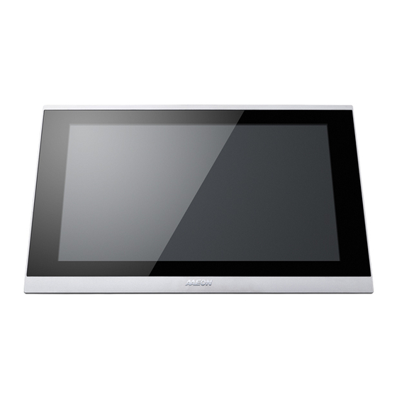
- Page 1 OMNI-2155-CML Industrial Touch Panel with 10 Generation Intel® Core™ Processors User’s Manual 1 Last Updated: May 14, 2021...
- Page 2 Copyright Notice This document is copyrighted, 2021. All rights are reserved. The original manufacturer reserves the right to make improvements to the products described in this manual at any time without notice. No part of this manual may be reproduced, copied, translated, or transmitted in any form or by any means without the prior written permission of the original manufacturer.
- Page 3 Acknowledgement All other product name or trademarks are properties of their respective owners. Microsoft Windows® is a registered trademark of Microsoft Corp. ⚫ Intel®, Pentium®, and Celeron® are registered trademarks of Intel ⚫ Corporation Intel Core™ is a trademark of Intel Corporation ⚫...
- Page 4 Packing List Before setting up your product, please make sure the following items have been shipped: Item Quantity OMNI-2155-CML ⚫ Screw Package ⚫ 3 Pin DC-In Power Connector ⚫ If any of these items are missing or damaged, please contact your distributor or sales representative immediately.
- Page 5 About this Document This User’s Manual contains all the essential information, such as detailed descriptions and explanations on the product’s hardware and software features (if any), its specifications, dimensions, jumper/connector settings/definitions, and driver installation instructions (if any), to facilitate users in setting up their product. Users may refer to the product page at AAEON.com for the latest version of this document.
- Page 6 Safety Precautions Please read the following safety instructions carefully. It is advised that you keep this manual for future references All cautions and warnings on the device should be noted. Make sure the power source matches the power rating of the device. Position the power cord so that people cannot step on it.
- Page 7 If any of the following situations arises, please the contact our service personnel: Damaged power cord or plug Liquid intrusion to the device iii. Exposure to moisture Device is not working as expected or in a manner as described in this manual The device is dropped or damaged Any obvious signs of damage displayed on the device...
- Page 8 FCC Statement This device complies with Part 15 FCC Rules. Operation is subject to the following two conditions: (1) this device may not cause harmful interference, and (2) this device must accept any interference received including interference that may cause undesired operation. Caution: There is a danger of explosion if the battery is incorrectly replaced.
- Page 9 China RoHS Requirements (CN) 产品中有毒有害物质或元素名称及含量 AAEON System QO4-381 Rev.A0 有毒有害物质或元素 部件名称 铅 汞 镉 六价铬 多溴联苯 多溴二苯 醚(PBDE) (Pb) (Hg) (Cd) (Cr(VI)) (PBB) 印刷电路板 × ○ ○ ○ ○ ○ 及其电子组件 外部信号 × ○ ○ ○ ○ ○ 连接器及线材 ○ ○...
- Page 10 China RoHS Requirement (EN) Hazardous and Toxic Materials List AAEON System QO4-381 Rev.A0 Hazardous or Toxic Materials or Elements Component Name PCB and Components Wires & Connectors for Ext.Connections Chassis CPU & RAM HDD Drive LCD Module Optical Drive Touch Control Module Battery This form is prepared in compliance with the provisions of SJ/T 11364.
-
Page 11: Table Of Contents
Table of Contents Chapter 1 - Product Specifications ..................1 Specifications ......................2 Chapter 2 – Hardware Information ..................5 Dimensions ......................6 Jumpers and Connectors ..................8 List of Jumpers ......................9 2.3.1 Clear CMOS (JP1) ..................9 2.3.2 LVDS BKLT Power (JP2) ................ - Page 12 2.4.15 USB2.0 Wafer Box (5P Pitch: 1.25mm) (CN17/CN18) ...... 19 2.4.16 USB3.2 Gen 2 Connector (CN19/CN20) ........... 20 2.4.17 Speaker (CN21) ..................21 2.4.18 Line Out (CN22) ..................21 2.4.19 Speaker (CN23) ..................22 2.4.20 Audio I/O Port (10P Pitch: 1.25mm) ..........22 2.4.21 Power Input 3-pin Terminal Block ............
- Page 13 3.4.5 NVMe Configuration ................46 3.4.5.1 NVMe Configuration: Device ..........47 3.4.6 USB Configuration ................48 3.4.7 Hardware Monitor ................49 3.4.8 SIO Configuration ................. 50 3.4.8.1 SIO Configuration: Serial Port 1 ..........51 3.4.8.2 SIO Configuration: Serial Port 2 ........... 52 3.4.9 Power Management ................
-
Page 14: Chapter 1 - Product Specifications
Chapter 1 Chapter 1 - Product Specifications... -
Page 15: Specifications
Specifications System Processor Intel® Core™ i9-10900TE Intel® Core™ i7-10700TE Intel® Core™ i5-10500TE Intel® Core™ i3-10100TE Intel® Celeron® G5900TE System Memory DDR4 SO-DIMM x 2, up to 64GB LCD/CRT Controller — Ethernet Intel® i211 x 1 Intel® i219 x 1 I/O Port HDMI x 1 RJ-45 x 2 for GbE LAN (i211 x 1, i219 x 1) USB 3.2 Gen 2 x 4... - Page 16 Mechanical Construction Aluminum Design (IP65 Front Frame) Mounting VESA 100 / Panel Mount Dimension 420.14mm x 264.47mm x 73.2mm Carton Dimension 530mm x 445mm x 200mm Gross Weight 6.75 kg Environmental Operating Temperature 0°C ~ 45°C (35W CPU), according to IEC68-2-14 with 0.5 m/s airflow Storage Temperature -4°F ~ 158°F (-20°C ~ 70°C)
- Page 17 Touchscreen Type Flat 5-wire Resistive / P-CAP Multi Touch Light Transmission 80% ± 3% / 88%± 2% Chapter 1 – Product Specifications...
-
Page 18: Chapter 2 - Hardware Information
Chapter 2 Chapter 2 – Hardware Information... -
Page 19: Dimensions
Dimensions Main Panel Chapter 2 – Hardware Information... - Page 20 Board Dimensions Chapter 2 – Hardware Information...
-
Page 21: Jumpers And Connectors
Jumpers and Connectors Chapter 2 – Hardware Information... -
Page 22: List Of Jumpers
List of Jumpers Please refer to the table below for all of the system’s jumpers that you can configure for your application Label Function Clear CMOS LVDS BKLT Power LVDS BKLT Control Selection 4,5,8 Wire Selection Auto Power Button Selection 2.3.1 Clear CMOS (JP1) Normal (Default) -
Page 23: 4,5,8 Wire Selection
2.3.4 4,5,8 Wire Selection 4,8 Wire 5 Wire (Default) 2.3.5 Auto Power Button Selection (JP3) 1 2 3 ATX (Default) Chapter 2 – Hardware Information... -
Page 24: List Of Connectors
List of Connectors Please refer to the table below for all of the system’s connectors that you can configure for your application Label Function LVDS Port LVDS Inverter SATA Port HDMI Port VGA Port (Wafer) LAN RJ45 Port LAN RJ45 Port Touch Screen Lines LVDS Control Touch CN10... -
Page 25: Lvds Port (Cn1)
Label Function CN24 Audio (Wafer) CN26 Power Input 3P terminal block CN28 Panel ID CN29 SATA Power CN55 COM4 Port (Wafer) CN61 COM3 Port (Wafer) Front Panel LPC1 Low Pin Count PCIE1 PCIe Slot SIM1 SIM card slot Power Button 2.4.1 LVDS Port (CN1) Signal... -
Page 26: Lvds Inverter
Signal Signal LVD_B_TXN3 LVD_B_TXP3 LVDSVCC LVD_B_CLKN LVD_B_CLKP 2.4.2 LVDS Inverter (CN2 Signal Signal BKL_CTL BKL_EN 2.4.3 SATA Port (CN3) Pin Name Signal Type Signal Level SATA_TX+ DIFF SATA_TX- DIFF SATA_RX- DIFF SATA_RX+ DIFF Chapter 2 – Hardware Information... -
Page 27: Hdmi Port (Cn4)
2.4.4 HDMI Port (CN4) CN4 HDMI Port follows standard specifications. 2.4.5 VGA Port (Wafer Box, Optional) Signal Signal VSYNC HSYNC GREEN DDC_CLK DDC_DAT BLUE 2.4.6 LAN1/LAN2 Port (CN6/CN7) Pin Name Signal Type Signal Level MDI0+ DIFF MDI0- DIFF MDI1+ DIFF MDI1- DIFF MDI2+... -
Page 28: Touch Screen Lines (Cn8)
Pin Name Signal Type Signal Level MDI2- DIFF MDI3+ DIFF MDI3- DIFF 2.4.7 Touch Screen Lines (CN8) Signal Signal TOP EXCITE BOTTOM EXCITE LEFT EXCITE RIGHT EXCITE TOP SENSE BOTTOM SENSE LEFT SENSE RIGHT SENSE 2.4.8 NGFF (M-Key) 2280 (CN10) CN10 M.2 M-Key follows standard specifications Chapter 2 –... -
Page 29: Ngff (E-Key) 2230 (Cn11)
2.4.9 NGFF (E-Key) 2230 (CN11) CN11 M.2 E-Key follows standard specifications 2.4.10 Power Button (Wafer, Reserve) (CN12) Pin Name FP_PANSWH# 2.4.11 SPI Flash Port (CN13) Pin Name Signal Type Signal Level SPI_MISO SPI_CLK +3.3VSB +3.3V SPI_MOSI SPI_CS Chapter 2 – Hardware Information... -
Page 30: Dio Port (Cn14)
2.4.12 DIO Port (CN14) Pin Name Signal Type Signal Level DIO0 DIO1 DIO2 DIO3 DIO4 DIO5 DIO6 DIO7 Chapter 2 – Hardware Information... -
Page 31: Com1 Port (Cn15)
2.4.13 COM1 Port (CN15) Pin Name Signal Type Signal Level DCD1 ±9V DTR1 ±9V DSR1 RTS1 ±9V CTS1 Chapter 2 – Hardware Information... -
Page 32: Com2 Port (Cn16)
2.4.14 COM2 Port (CN16) Pin Name Signal Type Signal Level DCD2 ±9V DTR2 ±9V DSR2 RTS2 ±9V CTS2 2.4.15 USB2.0 Wafer Box (5P Pitch: 1.25mm) (CN17/CN18) Pin Name Signal Type Signal Level USBD- DIFF USBD+ DIFF Chapter 2 – Hardware Information... -
Page 33: Usb3.2 Gen 2 Connector (Cn19/Cn20)
2.4.16 USB3.2 Gen 2 Connector (CN19/CN20) Pin Name Signal Type Signal Level +5VSB USB1_D- DIFF USB1_D+ DIFF USB1_SSRX− DIFF USB1_SSRX+ DIFF USB1_SSTX− DIFF USB1_SSTX+ DIFF +5VSB USB2_D- DIFF USB2_D+ DIFF USB2_SSRX− DIFF USB2_SSRX+ DIFF USB2_SSTX− DIFF USB2_SSTX+ DIFF Chapter 2 – Hardware Information... -
Page 34: Speaker (Cn21)
2.4.17 Speaker (CN21) Pin Name SPK-L- SPK-L+ 2.4.18 Line Out (CN22) Pin Name Pin Name AUD_GND LOUT_R HP_DET LOUT_L Chapter 2 – Hardware Information... -
Page 35: Speaker (Cn23)
2.4.19 Speaker (CN23) Pin Name SPK-R- SPK-R+ 2.4.20 Audio I/O Port (10P Pitch: 1.25mm) Pin Name Signal Type Signal Level MIC_L MIC_R GND_AUDIO LINE_L_IN LINE_R_IN GND_AUDIO LEFT_OUT GND_AUDIO Chapter 2 – Hardware Information... -
Page 36: Power Input 3-Pin Terminal Block
Pin Name Signal Type Signal Level RIGHT_OUT +5V_AUDIO 2.4.21 Power Input 3-pin Terminal Block Pin Name Signal Type Signal Level +10V~+35V GND_EARTH 2.4.22 DIO (Panel ID) Port (CN28) Pin Name Signal Type Signal Level PANEL_ID1 PANEL_ID2 PANEL_ID3 Chapter 2 – Hardware Information... -
Page 37: Sata Power Connector (Cn29)
Pin Name Signal Type Signal Level PANEL_ID4 PANEL_ID5 PANEL_ID6 PANEL_ID7 PANEL_ID8 2.4.23 SATA Power Connector (CN29) Pin Name Signal Type Signal Level +12V +12V Chapter 2 – Hardware Information... -
Page 38: Com4 Port (Wafer Box, Optional) (Cn55)
2.4.24 COM4 Port (Wafer Box, Optional) (CN55) Pin Name Signal Type Signal Level DCD4 DSR4 RTS4 ±9V ±9V CTS4 DTR4 ±9V Chapter 2 – Hardware Information... -
Page 39: Com3 Port (Wafer Box, Optional) (Cn61)
2.4.25 COM3 Port (Wafer Box, Optional) (CN61) Pin Name Signal Type Signal Level DCD3 DSR3 RTS3 ±9V ±9V CTS3 DTR3 ±9V Chapter 2 – Hardware Information... -
Page 40: Front Panel (Jp7)
2.4.26 Front Panel (JP7) Pin Name Pin Name EXT_PWRBTN# SATA_LED# 3.3V FP_SPKR- PWRLED+ HWRST# 2.4.27 LPC Port (LPC1) LAD0 LAD1 LAD2 LAD3 +3.3V LFRAME# LRESET# LCLK LDRQ0 LDRQ1 SERIRQ Pin Name Signal Type Signal Level LAD0 +3.3V LAD1 +3.3V LAD2 +3.3V LAD3 +3.3V... -
Page 41: Mini Card Slot (Full-Sized) (Pcie1)
Pin Name Signal Type Signal Level LFRAME# LRESET# +3.3V LCLK LDRQ0 LDRQ1 SERIRQ +3.3V 2.4.28 Mini Card Slot (Full-Sized) (PCIe1) Pin Name Signal Type Signal Level PCIE_WAKE# +3.3V +3.3V +1.5V +1.5V PCIE_CLK_REQ# Chapter 2 – Hardware Information... - Page 42 Pin Name Signal Type Signal Level PCIE_REF_CLK- DIFF PCIE_REF_CLK+ DIFF W_DISABLE# +3.3V PCIE_RST# +3.3V PCIE_RX- DIFF +3.3VSB +3.3V PCIE_RX+ DIFF +1.5V +1.5V SMB_CLK +3.3V PCIE_TX- DIFF SMB_DATA +3.3V PCIE_TX+ DIFF USB_D- DIFF Chapter 2 – Hardware Information...
-
Page 43: Sim Slot (Sim1)
Pin Name Signal Type Signal Level USB_D+ DIFF +3.3VSB +3.3V +3.3VSB +3.3V +1.5V +1.5V +3.3VSB +3.3V 2.4.29 SIM Slot (SIM1) Pin Name Signal Type Signal Level UIM_PWR UIM_RST UIM_CLK UIM_VPP UIM_DATA Chapter 2 – Hardware Information... -
Page 44: Cpu Installation
CPU Installation The OMNI-2155-CML utilizes a socket-type CPU configuration, allowing users to easily change or upgrade CPUs within the same socket-type. Before starting CPU installation, be sure the system is powered down (not in sleep mode) and the power has been disconnected. Also, make sure the CPU is ready for installation. -
Page 45: Ram And 2.5" Storage Drive Installation
RAM and 2.5” Storage Drive installation Before starting RAM and Storage Drive installation, be sure the system is powered down (not in sleep mode) and the power has been disconnected. Also, make sure the components are ready for installation. It is best to perform installation on a flat surface, with the system removed from its mounting. - Page 46 Step 5: Mount the 2.5” Storage Device to the mounting bracket, securing with four screws. Step 6: Secure the bracket to the chassis as shown in the diagram. Step 7: Reattach the system to the panel, securing with the screws removed in Step 1. Chapter 2 –...
-
Page 47: Chapter 3 - Ami Bios Setup
Chapter 3 Chapter 3 - AMI BIOS Setup... -
Page 48: System Test And Initialization
System Test and Initialization The system uses certain routines to perform testing and initialization during the boot up sequence. If an error, fatal or non-fatal, is encountered, the system will output a few short beeps or an error message. The board can usually continue the boot up sequence with non-fatal errors. -
Page 49: Ami Bios Setup
AMI BIOS Setup The AMI BIOS ROM has a pre-installed Setup program that allows users to modify basic system configurations, which is stored in the battery-backed CMOS RAM and BIOS NVRAM so that the information is retained when the power is turned off. To enter BIOS Setup, press <Del>... -
Page 50: Setup Submenu: Main
Setup Submenu: Main Chapter 3 – AMI BIOS Setup... -
Page 51: Setup Submenu: Advanced
Setup Submenu: Advanced Chapter 3 – AMI BIOS Setup... -
Page 52: Trusted Computing
3.4.1 Trusted Computing Options Summary Security Device Disable Support Enable Optimal Default, Failsafe Default Enables or Disables BIOS support for security device. O.S. will not show Security Device. TCG EFI protocol and INT1A interface will not be available. SHA-1 PCR Bank Disable Optimal Default, Failsafe Default Enable... - Page 53 Options Summary Storage Hierarchy Disable Enable Optimal Default, Failsafe Default Enable or Disable Storage Hierarchy Endorsement Disable Hierarchy Enable Optimal Default, Failsafe Default Enable or Disable Endorsement Hierarchy TPM2.0 UEFI Spec TCG_1_2 Version TCG_2 Optimal Default, Failsafe Default Select the TCG2 Spec Version Support, TCG_1_2: The Compatible mode for Win8/Win10, TCG_2: Support new TCG2 protocol and event format for Win10 or later.
-
Page 54: Cpu Configuration
3.4.2 CPU Configuration Options Summary Intel (VMX) Virtualization Disabled Technology Enabled Optimal Default, Failsafe Default When enabled, a VMM can utilize the additional hardware capabilities provided by Vanderpool Technology. Active Processor Cores Optimal Default, Failsafe Default Number of cores to enable in each processor package. Intel®... -
Page 55: Pch-Fw Configuration
3.4.3 PCH-FW Configuration Options Summary ME State Disabled Enabled Optimal Default, Failsafe Default When Disabled ME will be put into ME Temporarily Disabled Mode. AMT BIOS Features Disabled Enabled Optimal Default, Failsafe Default When disabled AMT BIOS Features are no longer supported and user is no longer able to access MEBx Setup. -
Page 56: Firmware Update Configuration
3.4.3.1 Firmware Update Configuration Options Summary Me FW Image Re-Flash Disabled Optimal Default, Failsafe Default Enabled Enable/Disable ME FW Image Re-Flash function. FW Update Disabled Enabled Optimal Default, Failsafe Default Enable/Disable ME FW Update function. Chapter 3 – AMI BIOS Setup... -
Page 57: Ptt Configuration
3.4.3.2 PTT Configuration Options Summary TPM Device Selection dTPM Optimal Default, Failsafe Default Selects TPM device: PTT or dTPM. PTT – Enables in SkuMgr dTPM 1.2 – Disables PTT in SkuMgr Warning! PTT/dTPM will be disabled and all data saved on it will be lost. Chapter 3 –... -
Page 58: Sata Configuration
3.4.4 SATA Configuration Options Summary Disabled Enabled Optimal Default, Failsafe Default Enable or Disable SATA Port. Mini Card Disabled Enabled Optimal Default, Failsafe Default Enable or Disable SATA Port. Port Disabled Enabled Optimal Default, Failsafe Default Enable or Disable SATA Port. Chapter 3 –... -
Page 59: Nvme Configuration
3.4.5 NVMe Configuration Choose the device to be configured. Chapter 3 – AMI BIOS Setup... -
Page 60: Nvme Configuration: Device
3.4.5.1 NVMe Configuration: Device Options Summary Self Test Option Short Optimal Default, Failsafe Default Extended Select either Short or Extended Self Test. Short option will take couple of minutes and extended option will take several minutes to complete. Self Test Action Controller Only Test Optimal Default, Failsafe Default Controller and... -
Page 61: Usb Configuration
3.4.6 USB Configuration Options Summary XHCI Hand-off Disabled Enabled Optimal Default, Failsafe Default This is a workaround for OSes without XHCI hand-off support. The XHCI ownership change should be claimed by XHCI driver. USB Mass Storage Driver Disabled Support Enabled Optimal Default, Failsafe Default Enable/Disable USB Mass Storage Driver Support. -
Page 62: Hardware Monitor
3.4.7 Hardware Monitor Chapter 3 – AMI BIOS Setup... -
Page 63: Sio Configuration
3.4.8 SIO Configuration Options Summary [*Active*] Serial Port N View and Set Basic properties of the SIO Logical device. Like IO Base, IRQ Range, DMA Channel and Device Mode. Chapter 3 – AMI BIOS Setup... -
Page 64: Sio Configuration: Serial Port 1
3.4.8.1 SIO Configuration: Serial Port 1 Options Summary Use This Device Disabled Enabled Optimal Default, Failsafe Default Enable or Disable this Logical Device. Possible Use Automatic Settings Optimal Default, Failsafe Default IO=3F8h; IRQ=4; IO=2F8h; IRQ=3; Allows the user to change the device resource settings. New settings will be reflected on this setup page after system restarts. -
Page 65: Sio Configuration: Serial Port 2
3.4.8.2 SIO Configuration: Serial Port 2 Options Summary Use This Device Disabled Enabled Optimal Default, Failsafe Default Enable or Disable this Logical Device. Possible Use Automatic Settings Optimal Default, Failsafe Default IO=2F8h; IRQ=3; IO=3F8h; IRQ=4; Allows the user to change the device resource settings. New settings will be reflected on this setup page after system restarts. -
Page 66: Power Management
3.4.9 Power Management Options Summary Power Mode ATX Type Optimal Default, Failsafe Default AT Type Select power supply mode. Restore AC Power Loss Last State Optimal Default, Failsafe Default Always On Always Off Select power state when power is re-applied after a power failure. RTC wake system from Disabled Optimal Default, Failsafe Default... -
Page 67: Setup Submenu: Chipset
Setup Submenu: Chipset Chapter 3 – AMI BIOS Setup... -
Page 68: System Agent (Sa) Configuration
3.5.1 System Agent (SA) Configuration Options Summary SA GV Disabled Fixed Low Fixed High Enabled Optimal Default, Failsafe Default System Agent Geyserville. Fixed Low/High: SA GV disabled, MRC only runs tasks from Low or High point. SA GV will be disabled on DT/Halo CPUs, regardless of this setting. PM Support Enabled Optimal Default, Failsafe Default... - Page 69 Options Summary VT-d Disabled Optimal Default, Failsafe Default Enabled VT-d capability Skip Scanning of Disabled Optimal Default, Failsafe Default External Gfx Card Enabled If Enable, it will not scan for External Gfx Card on PEG and PCH PCIE Ports. Chapter 3 – AMI BIOS Setup...
-
Page 70: Lvds Panel Configuration
3.5.1.1 LVDS Panel Configuration Options Summary Panel Type Selection Auto Optimal Default, Failsafe Default Manual Select LCD panel type by OMNI panel ID. Backlight Level 10% ~ 100 % step 10 % Default: 80% Select backlight control level. Backlight PWM Freq 100 Hz Default 220 Hz 200 Hz... -
Page 71: Pch-Io Configuration
3.5.2 PCH-IO Configuration Options Summary HD Audio Disabled Enabled Optimal Default, Failsafe Default Control Detection of the HD-Audio device. Disabled = HDA will be unconditionally disabled Enabled = HDA will be unconditionally enabled. Mini Card mSATA/PCIe PCIe Optimal Default, Failsafe Default Selection mSATA Select mSATA or PCIe function for Mini-Card. - Page 72 Options Summary M.2 PCIe Speed Auto Optimal Default, Failsafe Default Gen1 Gen2 Gen3 Configure PCIe Speed. Chapter 3 – AMI BIOS Setup...
-
Page 73: Setup Submenu: Security
Setup Submenu: Security Change User/Administrator Password You can set an Administrator Password or User Password. An Administrator Password must be set before you can set a User Password. The password will be required during boot up, or when the user enters the Setup utility. A User Password does not provide access to many of the features in the Setup utility. -
Page 74: Secure Boot
3.6.1 Secure Boot Options Summary Secure Boot Disabled Optimal Default, Failsafe Default Enabled Secure Boot feature is Active if Secure Boot is Enabled, Platform Key (PK) is enrolled and the System is in User mode. The mode change requires platform reset Secure Boot Mode Standard Custom... -
Page 75: Key Management
3.6.1.1 Key Management Options Summary Provision Factory Disabled Optimal Default, Failsafe Default Defaults Enabled Install factory default Secure Boot keys after the platform reset and while the System is in Setup mode. Restore Factory Keys Force system to user mode. Install factory default Secure Boot key databases. - Page 76 Secure Boot Variables Enroll Factory Defaults or load certificates from a file: 1. Public Key Certificate in: a) EFI_SIGNATURE_LIST b) EFI_CERT_X509 (DER encoded) c) EFI_CERT_RSA2048 (bin) d) EFI_CERT_SHA256,384,512 2. Authenticated UEFI Variable 3. EFI PE/COFF Image (SHA256) Key Source: Default, External, Mixed, Test Chapter 3 –...
-
Page 77: Setup Submenu: Boot
Setup Submenu: Boot Options Summary Quiet Boot Disabled Enabled Optimal Default, Failsafe Default Enable / Disable Quiet Boot option. Network Stack Enabled Disabled Optimal Default, Failsafe Default Enable/Disable UEFI Network Stack. FIXED BOOT ORDER Sets the system boot order. Priorities Chapter 3 –... -
Page 78: Setup Submenu: Save & Exit
Setup Submenu: Save & Exit Chapter 3 – AMI BIOS Setup... -
Page 79: Chapter 4 - Drivers Installation
Chapter 4 Chapter 4 – Drivers Installation... -
Page 80: Drivers Download And Installation
Drivers Download and Installation Drivers for the OMNI-2155-CML can be downloaded from the product page on the AAEON website by following this link: [add link once website is ready] Download the driver(s) you need and follow the steps below to install them. Step 1 –... - Page 81 Step 4 – Install LAN Drivers Open the Step 4 – LAN folder and select your OS Open the PROWinx64.exe file in the folder Follow the instructions Drivers will be installed automatically Step 5 – Install Audio Drivers Open the Step 5 – Audio folder and select your OS Open the 0008-64bit_Win7_Win8_Win81_Win10_R281.exe file in the folder Follow the instructions Drivers will be installed automatically...
-
Page 82: Appendix A - Watchdog Timer Programming
Appendix A Appendix A - Watchdog Timer Programming... -
Page 83: Watchdog Timer Initial Program
Watchdog Timer Initial Program Table 1 : Super I/O relative register table Default Value Note SIO MB PnP Mode Index Register Index 0x2E(Note1) 0x2E or 0x4E SIO MB PnP Mode Data Register Data 0x2F(Note2) 0x2F or 0x4F Table 2 : Watchdog relative register table Register BitNum Value... - Page 84 ******************************************************************************** // SuperIO relative definition (Please reference to Table 1) #define byte SIOIndex //This parameter is represented from Note1 #define byte SIOData //This parameter is represented from Note2 #define void IOWriteByte(byte IOPort, byte Value); #define byte IOReadByte(byte IOPort); // Watch Dog relative definition (Please reference to Table 2) #define byte TimerLDN //This parameter is represented from Note3 #define byte TimerReg //This parameter is represented from Note4 #define byte TimerVal // This parameter is represented from Note24...
-
Page 85: Appendix B - I/O Information
Appendix B Appendix B - I/O Information... -
Page 86: I/O Address Map
I/O Address Map Appendix B – I/O Information... - Page 87 Appendix B – I/O Information...
- Page 88 Appendix B – I/O Information...
-
Page 89: Memory Address Map
Memory Address Map Appendix B – I/O Information... - Page 90 Appendix B – I/O Information...
-
Page 91: Irq Mapping Chart
IRQ Mapping Chart Appendix B – I/O Information... - Page 92 Appendix B – I/O Information...
- Page 93 Appendix B – I/O Information...
- Page 94 Appendix B – I/O Information...
- Page 95 Appendix B – I/O Information...
- Page 96 Appendix B – I/O Information...
- Page 97 Appendix B – I/O Information...
- Page 98 Appendix B – I/O Information...
- Page 99 Appendix B – I/O Information...
- Page 100 Appendix B – I/O Information...
- Page 101 Appendix B – I/O Information...
- Page 102 Appendix B – I/O Information...
- Page 103 Appendix B – I/O Information...