
Summary of Contents for Asus AAEON FWS-2365
- Page 1 FWS-2365 Desktop Network Appliance User Manual 1 Last Updated: January 7, 2021...
- Page 2 Copyright Notice This document is copyrighted, 2021. All rights are reserved. The original manufacturer reserves the right to make improvements to the products described in this manual at any time without notice. No part of this manual may be reproduced, copied, translated, or transmitted in any form or by any means without the prior written permission of the original manufacturer.
- Page 3 Acknowledgement All other products’ name or trademarks are properties of their respective owners. Intel® is a registered trademark of Intel Corporation ⚫ Intel Atom™ is a registered trademark of Intel Corporation ⚫ ITE is a trademark of Integrated Technology Express, Inc. ⚫...
- Page 4 Packing List Before setting up your product, please make sure the following items have been shipped: Item Quantity FWS-2365 ⚫ SATA Cable ⚫ SATA Power Cable ⚫ 40W Power Adapter (C3558 SKU) ⚫ If any of these items are missing or damaged, please contact your distributor or sales representative immediately.
- Page 5 About this Document This User’s Manual contains all the essential information, such as detailed descriptions and explanations on the product’s hardware and software features (if any), its specifications, dimensions, jumper/connector settings/definitions, and driver installation instructions (if any), to facilitate users in setting up their product. Users may refer to the product page at AAEON.com for the latest version of this document.
- Page 6 Safety Precautions Please read the following safety instructions carefully. It is advised that you keep this manual for future references All cautions and warnings on the device should be noted. All cables and adapters supplied by AAEON are certified and in accordance with the material safety laws and regulations of the country of sale.
- Page 7 As most electronic components are sensitive to static electrical charge, be sure to ground yourself to prevent static charge when installing the internal components. Use a grounding wrist strap and contain all electronic components in any static-shielded containers. If any of the following situations arises, please the contact our service personnel: Damaged power cord or plug Liquid intrusion to the device iii.
- Page 8 FCC Statement This device complies with Part 15 FCC Rules. Operation is subject to the following two conditions: (1) this device may not cause harmful interference, and (2) this device must accept any interference received including interference that may cause undesired operation. Caution: There is a danger of explosion if the battery is incorrectly replaced.
- Page 9 China RoHS Requirements (CN) 产品中有毒有害物质或元素名称及含量 AAEON System QO4-381 Rev.A0 有毒有害物质或元素 部件名称 铅 汞 镉 六价铬 多溴联苯 多溴二苯 醚(PBDE) (Pb) (Hg) (Cd) (Cr(VI)) (PBB) 印刷电路板 × ○ ○ ○ ○ ○ 及其电子组件 外部信号 × ○ ○ ○ ○ ○ 连接器及线材 ○ ○...
- Page 10 China RoHS Requirement (EN) Hazardous and Toxic Materials List AAEON System QO4-381 Rev.A0 Hazardous or Toxic Materials or Elements Component Name PCB and Components Wires & Connectors for Ext.Connections Chassis CPU & RAM HDD Drive LCD Module Optical Drive Touch Control Module Battery This form is prepared in compliance with the provisions of SJ/T 11364.
-
Page 11: Table Of Contents
Table of Contents Chapter 1 – Product Specifications ..................14 Specifications ......................15 Chapter 2 – Hardware Information ..................18 Dimensions ......................19 Jumpers and Connectors ................... 22 List of Jumpers ...................... 23 2.3.1 Clear CMOS (CN2) ................... 23 List of Connectors ....................24 2.4.1 System Configuration Notes .............. - Page 12 3.4.2.2 Legacy Console Redirection Settings........48 3.4.2.3 Out of Band Management Port/Windows EMS ....49 3.4.3 USB Configuration ..................51 3.4.4 SIO Configuration ..................52 3.4.4.1 Serial Port Configuration ............53 3.4.5 Hardware Monitor ..................54 3.4.6 LAN Bypass Configuration ..............56 3.4.7 Power Management ................
- Page 13 B.1.3 Sample Code ..................... 87 LAN Bypass......................89 B.2.1 Introduction ....................89 B.2.1 LAN Bypass Configuration ..............89 B.2.3 Sample Code ....................91 Software Reset Button (General Propose Input) ..........94 B.3.1 Introduction ....................94 B.3.2 Soft Reset Button Configuration ............94 B.3.3 Sample Code .....................
-
Page 14: Chapter 1 - Product Specifications
Chapter 1 Chapter 1 – Product Specifications... -
Page 15: Specifications
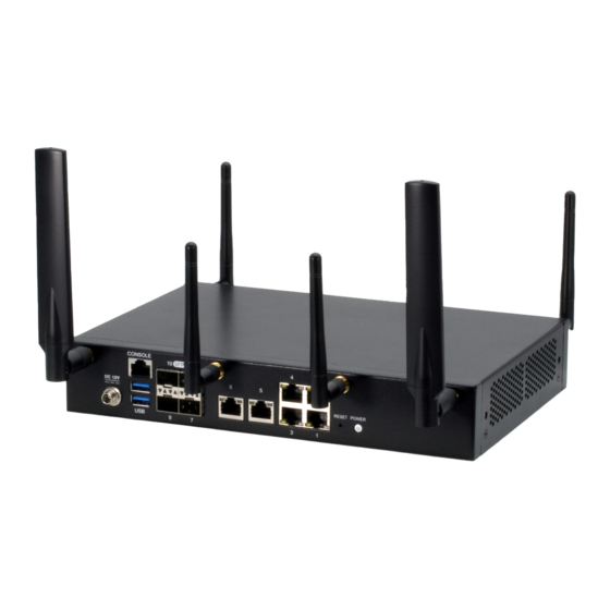
Specifications System Form Factor Desktop Processor Intel® Atom™ Processor C3000 series (4~16 cores) Chipset System Memory DDR4 SODIMM socket x 2 Network Ethernet 1GbE RJ-45 x 6 (2 ports co-lay SFP) 10G SFP+ x 4 (4 core processors only support 2 SFP ports) Bypass Supports 1 pair on LAN Ports 3-4... - Page 16 Internal/Expansion Interface PCIe Slot — Expansion slot Half-sized Mini-card slot x 1 (PCIe) Full-sized Mini-card slot x 1 (PCIe + USB2.0) with SIM slot M.2 B key 3052 x 1 (USB3.0) with SIM slot KB/Mouse Reserved pin header USB 3.0 x 2 (1 Port only supports USB2.0 signal) Miscellaneous Internal RTC Watchdog Timer...
- Page 17 Physical & Environmental Vibration 0.5 g rms/ 5 ~ 500Hz / operation (2.5” HDD) 1.5 g rms/ 5 ~ 500Hz / non-operation Shock 10 G peak acceleration (11 m sec. duration), operation 20 G peak acceleration (11 m sec. duration), non-operation Dimension (W x D x H) 260mm x 178mm x 44mm...
-
Page 18: Chapter 2 - Hardware Information
Chapter 2 Chapter 2 – Hardware Information... -
Page 19: Dimensions
Dimensions System Chapter 2 – Hardware Information... - Page 20 Board Top and I/O View Chapter 2 – Hardware Information...
- Page 21 Bottom and Side View Chapter 2 – Hardware Information...
-
Page 22: Jumpers And Connectors
Jumpers and Connectors Top and I/O View Note: Components and their locations may vary depending upon which configuration was purchased. If you have questions about your FWS-2365, visit our website to contact an AAEON support representative. Chapter 2 – Hardware Information... -
Page 23: List Of Jumpers
List of Jumpers Please refer to the table below for all of the board’s jumpers that you can configure for your application Label Function Clear CMOS 2.3.1 Clear CMOS (CN2) Pins 1-3 and 2-4 Selected Pins 3-5 and 4-6 Selected Normal, Default Clear CMOS Note: To prevent damage to the system or unwanted operation, do not connect... -
Page 24: List Of Connectors
List of Connectors Please refer to the table below for all of the board’s connectors that you can configure for your application. (Optional) denotes a component that is not included on the standard configuration. Some optional components may replace standard components. - Page 25 Label Function CN28 10 Gbps SPF+ Connector LAN 2 Port Connector (4 Port Optional) CN29 LAN5 RJ45 Connector CN30 LAN6 RJ45 Connector LED5 LAN8 LED Indicator LED6 LAN7 LED Indicator LED11 LAN10 LED Indicator LED12 LAN9 LED Indicator LED13 LAN1 LED Indicator LED14 LAN2 LED Indicator LED15...
-
Page 26: System Configuration Notes
2.4.1 System Configuration Notes Expansion Card Slots Standard expansion slot configuration is CN21, SLOT1 and SLOT2. Optional expansion slots replace standard configuration per diagram in Chapter 2.2. M1, M2 SFP Connectors (Optional) Optional M1 and M2 SFP LAN Ports replace CN29, CN30 RJ45 LAN Ports in system configuration. -
Page 27: Digital Io Header (Cn11)
2.4.4 Digital IO Header (CN11) Signal Signal Digital IO bit1 Digital IO bit1 Digital IO bit2 Digital IO bit2 Digital IO bit3 Digital IO bit3 Digital IO bit4 Digital IO bit4 2.4.5 Front Panel Header (CN14) Signal Signal Power Button SW+ Hardware Reset SW+ Power LED+ Power LED-... -
Page 28: Dc Power In (Cn25)
2.4.6 DC Power In (CN25) Signal Signal +12V +12V Chapter 2 – Hardware Information... -
Page 29: Hardware Assembly
Hardware Assembly 2.5.1 Opening the System Before performing any hardware installation, make sure the system is powered down and not in sleep or suspended mode. Disconnect the power cable or connector and ensure there is no power to the system. Step 1: Remove the four screws (two on each side) securing the top panel. - Page 30 Step 2: Remove the top panel by first sliding it slightly, then lifting. Follow these steps in reverse to secure the top panel when finished with hardware installation. Ensure the top panel is secure and the screws are fastened snugly. Chapter 2 –...
-
Page 31: Installing The Dual 2.5" Drive Assembly
2.5.2 Installing the Dual 2.5” Drive Assembly Before beginning, ensure you have the following ready: two (2) dual 2.5” drive mounting brackets (L-bracket), eight (8) mounting cushions, eight (8) mounting screws, two (2) 2.5” SATA drives (HDD or SSD). Step 1: Follow the directions in the previous section for accessing the system. Step 2: Install the mounting cushions into the mounting holes as shown: Chapter 2 –... - Page 32 Step 3: Mount the two 2.5” drives to the mounting bracket. Not the direction, the flange on the mounting brackets will go under the drive assembly, and the drives should be mounted label side up. Chapter 2 – Hardware Information...
- Page 33 Step 4: Mount the drive assembly into the system. Secure with four screws mounted through the flange as shown. Please not the direction of the drives to ensure access to the SATA connectors. SATA and Power Connectors Chapter 2 – Hardware Information...
- Page 34 Step 5: Connect the bottom drive to the SATA1 connector and CN3 SATA Power Connector on the board (See Chapter 2.2 for reference). SATA1 Connector CN3 SATA Power Chapter 2 – Hardware Information...
- Page 35 Step 6: Repeat for the top drive, connecting to CN4 SATA Power connector and SATA2 Connector on the board. CN4 SATA Power SATA2 Connector Drive installation is complete. Reassemble the system following instructions in Chapter 2.5.1 or continue to the next section for Antenna Mount Assembly. Chapter 2 –...
-
Page 36: Antenna Mount Assembly
2.5.3 Antenna Mount Assembly Before beginning, ensure you have the following ready: two (2) antenna screw mounts with securing washer and nut, two (2) antenna mounting brackets, four (4) mounting screws. Step 1: Follow the directions in Chapter 2.5.1 for accessing the system. Step 2: Assemble the antenna mounts by placing the screw mounts into the mounting brackets and securing with washer and nut. - Page 37 Step 3: Mount the antennas to either side of the system chassis and secure with two screws each. Chapter 2 – Hardware Information...
-
Page 38: Chapter 3 - Ami Bios Setup
Chapter 3 Chapter 3 – AMI BIOS Setup... -
Page 39: System Test And Initialization
System Test and Initialization The system uses certain routines to perform testing and initialization during the boot up sequence. If an error, fatal or non-fatal, is encountered, the system will output a few short beeps or display an error message. The system can usually continue the boot up sequence with non-fatal errors. -
Page 40: Ami Bios Setup
AMI BIOS Setup The AMI BIOS ROM has a pre-installed Setup program that allows users to modify basic system configurations, which is stored in the battery-backed CMOS RAM and BIOS NVRAM so that the information is retained when the power is turned off. To enter BIOS Setup, press <Del>... -
Page 41: Setup Submenu: Main
Setup Submenu: Main Chapter 3 – AMI BIOS Setup... -
Page 42: Setup Submenu: Advanced
Setup Submenu: Advanced Options Summary Case Open Warning Disabled Optimal Default, Failsafe Default Enabled Clear Case Open detecting function Chapter 3 – AMI BIOS Setup... -
Page 43: Trusted Computing
3.4.1 Trusted Computing Options Summary Security Device Supp Disable Enable Optimal Default, Failsafe Default Enables or Disables BIOS support for security device. O.S. will not show Security Device. TCG EFI protocol and INT1A interface will not be available. Pending operation None Optimal Default, Failsafe Default TPM Clear... - Page 44 Options Summary Endorsement Hierarchy Disable Enable Optimal Default, Failsafe Default Enable or Disable Endorsement Hierarchy TPM2.0 UEFI Spec TCG_1_2 Version TCG_2 Optimal Default, Failsafe Default Select the TCG2 Spec Version Support, TCG_1_2: The Compatible mode for Win8/Win10 TCG_2: Support new TCG2 protocol and event Physical Presence Spec Version Optimal Default, Failsafe Default...
-
Page 45: Serial Port Console Redirection
3.4.2 Serial Port Console Redirection Options Summary COM0 Console Disabled Redirection Enabled Optimal Default, Failsafe Default Console Redirection Enable or Disable EMS Console Disabled Redirection Enabled Optimal Default, Failsafe Default Console Redirection Enable or Disable Chapter 3 – AMI BIOS Setup... -
Page 46: Com0 Console Redirection
3.4.2.1 COM0 Console Redirection Options Summary Terminal Type VT100 VY100+ VT-UTF8 ANSI Optimal Default, Failsafe Default Emulation: ANSI: Extended ASCII char set. VT100: ASCII char set. VT100+: Extends VT100 to support color, function keys, etc. VT-UTF8: Uses UTF8 encoding to map Unicode. Bits per second 9600 19200... - Page 47 Options Summary Data bit Optimal Default, Failsafe Default Data Bits Parity None Optimal Default, Failsafe Default Even Mark Space A Parity bit can be sent with the data bits to detect some transmission errors. Even: parity bit is 0 if the num of 1’s in the data bits is even. Odd: parity bit is 0 if the num of 1’s in the data bits is odd.
-
Page 48: Legacy Console Redirection Settings
3.4.2.2 Legacy Console Redirection Settings Options Summary Redirection COM Port COM0 Optimal Default, Failsafe Default Select a COM port to display redirection of Legacy OS and Legacy OPROM Messages. Resolution 80x24 Optimal Default, Failsafe Default 80x25 On Legacy OS, the Number of Rows and Columns supported redirection. Redirection After POST Always Enable Optimal Default, Failsafe Default BootLoader... -
Page 49: Out Of Band Management Port/Windows Ems
3.4.2.3 Out of Band Management Port/Windows EMS Options Summary Terminal Type VT100 VY100+ VT-UTF8 Optimal Default, Failsafe Default ANSI VT-UTF8 is the preferred terminal type for out-of-band management. The next best choice is VT100+ and then VT100. See above, in Console Redirection Settings page, for more Help with Terminal Type/Emulation. - Page 50 Options Summary Flow control None Optimal Default, Failsafe Default Hardware RTS/CTS Software Xon/Xoff Flow control can prevent data loss from buffer overflow. When sending data, if the receiving buffers are full, a ‘stop’ signal can be sent to stop the data flow. Once the buffers are empty, a ‘start’...
-
Page 51: Usb Configuration
3.4.3 USB Configuration Options Summary Legacy USB Support Disabled Enabled Optimal Default, Failsafe Default Enables Legacy USB support. AUTO option disables legacy support if no USB devices are connected. DISABLE option will keep USB devices available only for EFI applications. Chapter 3 –... -
Page 52: Sio Configuration
3.4.4 SIO Configuration Chapter 3 – AMI BIOS Setup... -
Page 53: Serial Port Configuration
3.4.4.1 Serial Port Configuration Options Summary Use This Device Disabled Enabled Optimal Default, Failsafe Default Enable/Disable this Logical Device Possible: Use Automatic Settings Optimal Default, Failsafe Default IO=3F8; IRQ=4; DMA; IO=2C8; IRQ=11; DMA; Allow user to change Device’s Resource settings. New settings will be reflected on This Setup Page after System restarts. -
Page 54: Hardware Monitor
3.4.5 Hardware Monitor Options Summary System Fan Enabled Optimal Default, Failsafe Default Disabled For En/Disable System FAN Smart Control Enabled: FAN is running in accordance with user settings Disabled: FAN is always running with full speed FAN Control Mode Automatic Mode Optimal Default, Failsafe Default Manual Mode Manual Mode: Depends on PWM Duty... - Page 55 Options Summary Start Control Optimal Default, Failsafe Default Temperature Temperature Limit Value of FAN Start Control Full Speed Temperature 70 Optimal Default, Failsafe Default Temperature Limit Value of FAN Full Speed PWM Slope Optimal Default, Failsafe Default Slope PWM value/Degree C for FAN Speed Control Range: [1-15] Chapter 3 –...
-
Page 56: Lan Bypass Configuration
3.4.6 LAN Bypass Configuration Options Summary LAN Bypass Status LED LED OFF Optimal Default, Failsafe Default RED LED ON RED LED BLINK RED LED FAST BLINK GREEN LED ON GREEN LED BLINK GREEN LED FAST BLINK Configure LAN Bypass Status LED. Mode for Power-on ByPass PassTru... - Page 57 Options Summary WDT Configuration System Reset Optimal Default, Failsafe Default Force ByPass Configure WDT behavior, System Rest or Force Bypass Chapter 3 – AMI BIOS Setup...
-
Page 58: Power Management
3.4.7 Power Management Options Summary Power Mode ATX Type Optimal Default, Failsafe Default AT Type Select power supply mode. Restore AC Power Loss Last State Always On Optimal Default, Failsafe Default Always Off Select power state when power is re-applied after a power failure. RTC wake system from Disabled Optimal Default, Failsafe Default... -
Page 59: Digital Io Port Configuration
3.4.8 Digital IO Port Configuration Options Summary DIO Port1~4 Output Optimal Default, Failsafe Default Input Set DIO as Input or Output Output Level High Optimal Default, Failsafe Default Set output level when DIO pin is output DIO Port5~8 Output Input Optimal Default, Failsafe Default Set DIO as Input or Output Chapter 3 –... -
Page 60: Setup Submenu: Security
Setup Submenu: Security Change User/Administrator Password You can set an Administrator Password or User Password. An Administrator Password must be set before you can set a User Password. The password will be required during boot up, or when the user enters the Setup utility. A User Password does not provide access to many of the features in the Setup utility. -
Page 61: Secure Boot
3.5.1 Secure Boot Options Summary Enable Secure Boot Disabled Optimal Default, Failsafe Default Enabled Secure Boot activated when Platform Key (PK) is enrolled, System mode is User/Deployed, and CSM function is disabled. Secure Boot Mode Standard Custom Optimal Default, Failsafe Default Secure Boot mode selector: Standard/Custom. -
Page 62: Key Management
3.5.1.1 Key Management Options Summary Provision Factory Defaults Disabled Optimal Default, Failsafe Default Enabled Reset to Setup Mode Force system to setup mode – delete all Secure Boot key databases. Enroll Efi Image Allow the image to run in Secure Boot mode. Enroll SHA256 hash of the binary into Authorized Signature Database (db). - Page 63 Options Summary Secure Boot Variables Enroll Factory Defaults or load certificates from a file: 1. Public Key Certificate in: a) EFI_SIGNATURE_LIST b) EFI_CERT_X509 (DER encoded) c) EFI_CERT_RSA2048 (bin) d) EFI_CERT_SHA256,384,512 2. Authenticated UEFI Variable 3. EFI PE/COFF Image (SHA256) Key Source: Default, External, Mixed, Test Chapter 3 –...
-
Page 64: Setup Submenu: Boot
Setup Submenu: Boot Options Summary Quiet Boot Disabled Enabled Optimal Default, Failsafe Default Enable / Disable Quiet Boot option. CSM Support Enabled Optimal Default, Failsafe Default Disabled Enable/Disable CSM Support. Launch PXE Rom Disabled Optimal Default, Failsafe Default Enabled Controls the execution of UEFI and Legacy PXE OpROM. Network Stack Disabled Optimal Default, Failsafe Default... - Page 65 Options Summary UEFI Hard Disk Drive BBS Specifies the Boot Device Priority sequence from Priorities. available UEFI Hard Disk Drives. UEFI USB Drive BBS Specifies the Boot Device Priority sequence from Priorities. available UEFI USB Drives. SD Drive BBS Priorities. Specifies the Boot Device Priority sequence from available SD Drives.
-
Page 66: Setup Submenu: Save & Exit
Setup Submenu: Save & Exit Chapter 3 – AMI BIOS Setup... -
Page 67: Setup Submenu: Intel Rc Setup
Setup Submenu: Intel RC Setup Options Summary Relax Security Disabled Optimal Default, Failsafe Default Configuration Enabled Relaxes the security configuration to be able to use BIOS update tools. Chapter 3 – AMI BIOS Setup... -
Page 68: Processor Configuration
3.8.1 Processor Configuration Chapter 3 – AMI BIOS Setup... -
Page 69: Server Me Configuration
3.8.2 Server ME Configuration Chapter 3 – AMI BIOS Setup... -
Page 70: North Bridge Chipset Configuration
3.8.3 North Bridge Chipset Configuration Chapter 3 – AMI BIOS Setup... -
Page 71: South Bridge Chipset Configuration
3.8.4 South Bridge Chipset Configuration Chapter 3 – AMI BIOS Setup... -
Page 72: Sata Configuration
3.8.4.1 SATA Configuration Chapter 3 – AMI BIOS Setup... - Page 73 3.8.4.1.1 SATA Controller Options Summary Enable controller Disabled Enabled Optimal Default, Failsafe Default Enables/Disables SATA Controller if supported by current CPU SKU. Chapter 3 – AMI BIOS Setup...
- Page 74 3.8.4.1.1.1 SATA 1 Options Summary Enable controller Enabled Optimal Default, Failsafe Default Disabled Enables/Disables SATA Controller port if supported by current cpu SKU. Chapter 3 – AMI BIOS Setup...
- Page 75 3.8.4.1.1.2 SATA 2 Options Summary Enable controller Enabled Optimal Default, Failsafe Default Disabled Enables/Disables SATA Controller port if supported by current cpu SKU. Chapter 3 – AMI BIOS Setup...
-
Page 76: Chapter 4 - Driver Installation
Chapter 4 Chapter 4 – Driver Installation... -
Page 77: Driver Download And Installation
Driver Download and Installation Drivers for the FWS-2365 can be downloaded from the product page on the AAEON website by following this link: https://www.aaeon.com/en/p/white-box-desktop-network-appliance-fws-2365 Download the driver(s) you need and follow the steps below to install them. For Linux: LAN Driver Chapter 4 –... -
Page 78: Appendix A - Watchdog Timer Programming
Appendix A Appendix A – Watchdog Timer Programming... -
Page 79: Watchdog Timer Initial Program
Watchdog Timer Initial Program Table 1 : SuperIO relative register table Default Value Note SIO MB PnP Mode Index Register Index 0x2E(Note1) 0x2E or 0x4E SIO MB PnP Mode Data Register Data 0x2F(Note2) 0x2F or 0x4F Table 2 : Watchdog relative register table Register BitNum Value... - Page 80 ************************************************************************************ // SuperIO relative definition (Please reference to Table 1) #define byte SIOIndex //This parameter is represented from Note1 #define byte SIOData //This parameter is represented from Note2 #define void IOWriteByte(byte IOPort, byte Value); #define byte IOReadByte(byte IOPort); // Watch Dog relative definition (Please reference to Table 2) #define byte TimerLDN //This parameter is represented from Note3 #define byte TimerReg //This parameter is represented from Note4 #define byte TimerVal // This parameter is represented from Note24...
- Page 81 ************************************************************************************ Main VOID // Procedure : AaeonWDTConfig // (byte)Timer : Time of WDT timer.(0x00~0xFF) // (boolean)Unit : Select time unit(0: second, 1: minute). AaeonWDTConfig(); // Procedure : AaeonWDTEnable // This procudure will enable the WDT counting. AaeonWDTEnable(); ************************************************************************************ Appendix A – Watchdog Timer Programming...
- Page 82 ************************************************************************************ // Procedure : AaeonWDTEnable VOID AaeonWDTEnable (){ WDTEnableDisable(EnableLDN, EnableReg, EnableBit, 1); // Procedure : AaeonWDTConfig VOID AaeonWDTConfig (){ // Disable WDT counting WDTEnableDisable(EnableLDN, EnableReg, EnableBit, 0); // Clear Watchdog Timeout Status WDTClearTimeoutStatus(); // WDT relative parameter setting WDTParameterSetting(); VOID WDTEnableDisable(byte LDN, byte Register, byte BitNum, byte Value){ SIOBitSet(LDN, Register, BitNum, Value);...
- Page 83 ************************************************************************************ OID SIOEnterMBPnPMode(){ Switch(SIOIndex){ Case 0x2E: IOWriteByte(SIOIndex, 0x87); IOWriteByte(SIOIndex, 0x01); IOWriteByte(SIOIndex, 0x55); IOWriteByte(SIOIndex, 0x55); Break; Case 0x4E: IOWriteByte(SIOIndex, 0x87); IOWriteByte(SIOIndex, 0x01); IOWriteByte(SIOIndex, 0x55); IOWriteByte(SIOIndex, 0xAA); Break; VOID SIOExitMBPnPMode(){ IOWriteByte(SIOIndex, 0x02); IOWriteByte(SIOData, 0x02); VOID SIOSelectLDN(byte LDN){ IOWriteByte(SIOIndex, 0x07); // SIO LDN Register Offset = 0x07 IOWriteByte(SIOData, LDN);...
- Page 84 ************************************************************************************ VOID SIOBitSet(byte LDN, byte Register, byte BitNum, byte Value){ Byte TmpValue; SIOEnterMBPnPMode(); SIOSelectLDN(byte LDN); IOWriteByte(SIOIndex, Register); TmpValue = IOReadByte(SIOData); TmpValue &= ~(1 << BitNum); TmpValue |= (Value << BitNum); IOWriteByte(SIOData, TmpValue); SIOExitMBPnPMode(); VOID SIOByteSet(byte LDN, byte Register, byte Value){ SIOEnterMBPnPMode();...
-
Page 85: Appendix B - Hardware And Lan Bypass Programming
Appendix B Appendix B – Hardware and LAN Bypass Programming... -
Page 86: Status Led
Status LED B.1.1 Introduction The FWS-2365 features several LED indicators which can be programmed using the AAEON SDK. The user can program the LED indicators to display different status modes. B.1.2 Status LED Configuration Table1: LED Status STA_LED2 STA_LED1 STA_LED0 LED Status LED Off Red Blinking (Slowly) -
Page 87: Sample Code
B.1.3 Sample Code ************************************************************* #define Byte CPLD_SLAVE_ADDRESS //This parameter is represented from Note1 #define Byte OFFSET //This parameter is represented from Note2 ************************************************************* bData = aaeonSmbusReadByte(CPLD_SLAVE_ADDRESS, OFFSET); switch( LED_FLAG) case 0: //LED Off //BIT2=0, BIT1=0, BIT0=0 bData = bData & 0xF8; break;... - Page 88 //Green LED On //BIT2=1, BIT1=1, BIT0=1 bData = (bData & 0xF8) | 0x07; break; case 5: //Green LED Blink //BIT2=1, BIT1=0, BIT0=1 bData = (bData & 0xF8) | 0x05; break; case 6: //Green LED Fast Blink //BIT2=1, BIT1=1, BIT0=0 bData = (bData & 0xF8) | 0x06; break;...
-
Page 89: Lan Bypass
LAN Bypass B.2.1 Introduction The FWS-2365 supports LAN Bypass to allow uninterrupted network traffic even if a single in-line appliance is shut down or hangs. B.2.1 LAN Bypass Configuration Table1: LAN Kit ID Select LAN_ID2 LAN_ID1 LAN_ID0 LAN kit selected LAN Kit 1 Selected LAN Kit 2 Selected Table2: LAN Bypass relative register table... - Page 90 Table3: LAN Bypass relative register mapping table CPLD Slave Address 0x90 (Note1) Attribute Offset(SMBUS) BitNum Value LAN_ID3 0x01(Note2) (Table 1) LAN_ID2 0x01(Note2) (Table 1) LAN_ID1 0x01(Note2) (Table 1) LAN_ID0 0x01(Note2) (Table 1) PWR_ON 0x01(Note2) (Table 2) PWR_OFF 0x01(Note2) (Table 2) WDT_EN 0x01(Note2) (Table 2)
-
Page 91: Sample Code
B.2.3 Sample Code ************************************************************* #define Byte CPLD_SLAVE_ADDRESS //This parameter is represented from Note1 #define Byte OFFSET //This parameter is represented from Note2 ************************************************************* // Select Lan Pair BYTE bLanSel = LAN_PAIR; BYTE bData = SmbusReadByte(CPLD_SLAVE_ADDRESS, OFFSET); // Set Reg01h bit3 if(bLanSel &... - Page 92 else bData = bData & 0xFE; // Power On Action (Reg01h bit6) if(SET_PASS_THROUGH) // Pass Through bData = bData & 0xBF; else // Bypass bData = bData | 0x40; // Power Off Action (Reg01h bit5) if(SET_PASS_THROUGH) // Pass Through bData = bData & 0xDF; else // Bypass bData = bData | 0x20;...
- Page 93 SmbusWriteByte(CPLD_SLAVE_ADDRESS, OFFSET, bData | 0x80); ************************************************************* Appendix B – Hardware and LAN Bypass Programming...
-
Page 94: Software Reset Button (General Propose Input)
Software Reset Button (General Propose Input) B.3.1 Introduction The FWS-2365 features a general-purpose input button which can be programed with the AAEON SDK. B.3.2 Soft Reset Button Configuration Table 2: LAN Bypass relative register table Function Description Reading this register returns the pin level status which is normal high active low. -
Page 95: Sample Code
B.3.3 Sample Code ************************************************************* #define Word BTN_STS //This parameter is represented from Note1 #define Byte BTN_STS_R //This parameter is represented from Note2 ************************************************************* Byte GET_Value (Word IoAddr, Byte BitNum,Byte Value){ BYTE TmpValue; TmpValue = inportb (IoAddr); return (TmpValue & (1 << BitNum)) ************************************************************* VOID Main(){ Byte RstBtn;...