
Related Manuals for Asus Aaeon BOXER-6639M


Summary of Contents for Asus Aaeon BOXER-6639M
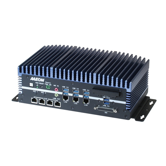
- Page 1 BOXER-6639M Fanless Embedded Box PC User’s Manual 1 Last Updated: September 28, 2017...
- Page 2 Copyright Notice This document is copyrighted, 2017. All rights are reserved. The original manufacturer reserves the right to make improvements to the products described in this manual at any time without notice. No part of this manual may be reproduced, copied, translated, or transmitted in any form or by any means without the prior written permission of the original manufacturer.
- Page 3 Acknowledgement All other products’ name or trademarks are properties of their respective owners. Microsoft Windows ® is a registered trademark of Microsoft Corp. Intel , Platium , Celeron , and Xeon are registered trademarks of Intel ® ® ® ®...
- Page 4 Packing List Before setting up your product, please make sure the following items have been shipped: Item Quantity BOXER-6639M Wallmount bracket Screw Package Thermal Pad Phoenix connector Product DVD with User’s Manual (in pdf) and drivers ...
- Page 5 About this Document This User’s Manual contains all the essential information, such as detailed descriptions and explanations on the product’s hardware and software features (if any), its specifications, dimensions, jumper/connector settings/definitions, and driver installation instructions (if any), to facilitate users in setting up their product. Users may refer to the AAEON.com for the latest version of this document.
- Page 6 Safety Precautions Please read the following safety instructions carefully. It is advised that you keep this manual for future references All cautions and warnings on the device should be noted. Make sure the power source matches the power rating of the device. Position the power cord so that people cannot step on it.
- Page 7 If any of the following situations arises, please the contact our service personnel: Damaged power cord or plug Liquid intrusion to the device iii. Exposure to moisture Device is not working as expected or in a manner as described in this manual The device is dropped or damaged Any obvious signs of damage displayed on the device...
- Page 8 FCC Statement This device complies with Part 15 FCC Rules. Operation is subject to the following two conditions: (1) this device may not cause harmful interference, and (2) this device must accept any interference received including interference that may cause undesired operation. Caution: There is a danger of explosion if the battery is incorrectly replaced.
- Page 9 China RoHS Requirements (CN) 产品中有毒有害物质或元素名称及含量 AAEON Embedded Box PC/ Industrial System 有毒有害物质或元素 部件名称 铅 汞 镉 六价铬 多溴联苯 多溴二苯醚 (Pb) (Hg) (Cd) (Cr(VI)) (PBB) (PBDE) 印刷电路板 ○ ○ ○ ○ ○ ○ 及其电子组件 外部信号 ○ ○ ○ ○ ○ ○ 连接器及线材...
- Page 10 China RoHS Requirement (EN) Poisonous or Hazardous Substances or Elements in Products AAEON Embedded Box PC/ Industrial System Poisonous or Hazardous Substances or Elements Hexavalent Polybrominated Polybrominated Component Lead Mercury Cadmium Chromium Biphenyls Diphenyl Ethers (Pb) (Hg) (Cd) (Cr(VI)) (PBB) (PBDE) PCB &...
-
Page 11: Table Of Contents
Table of Contents Chapter 1 - Product Specifications ..................1 Specifications ......................2 Chapter 2 – Hardware Information ..................5 Dimensions ......................6 2.1.1 I/O Location ..................... 8 Jumpers and Connectors ..................9 List of Jumpers ......................11 2.3.1 Auto Power Button (JP19) ..............11 2.3.2 Clear CMOS Jumper (JP24) .............. - Page 12 System Test and Initialization ................29 AMI BIOS Setup ....................30 Setup Submenu: Main ..................31 Setup Submenu: Advanced ................32 3.4.1 Advanced: CPU Configuration ............33 3.4.2 Advanced: Trusted Computing ............34 3.4.3 Advanced: SATA Configuration ............... 35 3.4.3 Advanced: PCH-FW Configuration ...........
- Page 13 Product CD/DVD ....................62 Appendix A - Watchdog Timer Programming..............64 Watchdog Timer Initial Program ............... 65 Appendix B - I/O Information ....................70 I/O Address Map ....................71 Memory Address Map ..................73 IRQ Mapping Chart ..................... 75 Appendix C - Digital I/O Information ................. 84 DIO Programming ....................
-
Page 14: Chapter 1 - Product Specifications
Chapter 1 Chapter 1 - Product Specifications... -
Page 15: Specifications
Specifications System 7th Generation Intel® CoreTM Processor family: Processor Intel® Core™ i7-7700T, 2.9 GHz Intel® Core™ i5-7500T, 2.8 GHz Intel® Core™ i3-7101TE, 3.4 GHz Intel® Pentium® G4600T, 3.0 GHz Intel® Pentium® G4560T, 2.9 GHz Intel® Celeron® G3930T, 2.7 GHz 6th Generation Intel®... - Page 16 USB 3.0 x 6 USB 2.0 x 2 DB-44 for 34-bit digital I/O (5V) Digital I/O Power LED x 1 LED Indicator Hard Disk Active LED x 1 Full-size Mini-Card x 2 Expansion Slot SIM Slot x 1 (for PCIE1) 7th Generation Intel®...
- Page 17 Gross Weight 5.9 kg (13.0 lb) Net Weight 4.0 kg (8.8 lb) Environmental Ambient with Airflow Operating Temperature -25°C ~ 55°C (according to IEC68-2-14 with 0.5 m/s AirFlow ; with industrial devices) Storage Temperature -45°C ~ 80°C (-49°F ~ 185°F) ...
-
Page 18: Chapter 2 - Hardware Information
Chapter 2 Chapter 2 – Hardware Information... -
Page 19: Dimensions
Dimensions Chapter 2 – Hardware Information... - Page 20 Chapter 2 – Hardware Information...
-
Page 21: I/O Location
2.1.1 I/O Location Chapter 2 – Hardware Information... -
Page 22: Jumpers And Connectors
Jumpers and Connectors Component Side Chapter 2 – Hardware Information... - Page 23 Solder Side Chapter 2 – Hardware Information...
-
Page 24: List Of Jumpers
List of Jumpers Please refer to the table below for all of the system’s jumpers that you can configure for your application. Label Function RS-232/ 422/ 485 selection for COM1 port RS-232/ 422/ 485 selection for COM6 port RS-232/ 422/ 485 selection for COM4 port RS-232/ 422/ 485 selection for COM3 port JP17 RS-232/ 422/ 485 selection for COM2 port... -
Page 25: List Of Connectors
List of Connectors Please refer to the table below for all of the system’s connectors that you can configure for your application Label Function DB-15 CRT port DC-IN 12~36V DC-IN connector HDMI1 HDMI connector HDMI2 HDMI connector 34- bit Digital Input & Output connector USB 3.0 Port 1~4 USB 3.0 Port USB 3.0 Port 5~6... -
Page 26: Vga Port
2.4.1 VGA Port Signal Signal Green Blue VGA_VCC DDC_DATA VGA_HSYNC VGA_VSYNC DDC_CLK 2.4.2 DC-IN Signal Signal PWR_IN Chapter 2 – Hardware Information... -
Page 27: Hdmi Port (Hdmi1/Hdmi2)
2.4.3 HDMI Port (HDMI1/HDMI2) Signal Signal HDMI_DATA2_P HDMI_DATA2_N HDMI_DATA1_P HDMI_DATA1_N HDMI_DATA0_P HDMI_DATA0_N HDMI_CLK_P HDMI_CLK_N HDMI_SCL HDMI_SDA HDMI_PWR HDMI_HDP 2.4.4 DIO Port Signal Signal DIO1 DIO2 DIO3 DIO4 DIO5 DIO6 Chapter 2 – Hardware Information... - Page 28 DIO7 DIO8 DIO9 DIO10 DIO11 DIO12 DIO13 DIO14 DIO15 DIO16 DIO17 DIO18 DIO19 DIO20 DIO21 DIO22 DIO23 DIO24 DIO25 DIO26 DIO27 DIO28 DIO29 DIO30 DIO31 DIO32 DIO33 DIO34 Chapter 2 – Hardware Information...
-
Page 29: Lan + Usb 3.0
2.4.5 LAN + USB 3.0 Signal Signal MDI0- MDI0+ MDI1+ MDI2+ MDI2- MDI1- MDI3+ MDI3- VBUS_2 VBUS_1 (B)D- (A)D- (A)D+ (B)D+ (A)SSRX- (B)SSRX- (A)SSRX+ (B)SSRX+ (A)SSTX- (B)SSTX- (A)SSTX+ (B)SSTX+ Chapter 2 – Hardware Information... -
Page 30: Remote Power Button
2.4.6 Remote Power Button Signal Signal PANSWH# 2.4.7 CFast Signal Signal +3.3V +3.3V Chapter 2 – Hardware Information... -
Page 31: Sata Power Connector 1~2
2.4.8 SATA Power Connector 1~2 Pin Name level +12V 2.4.9 SATA Signal Connector 1~2 Pin name Signal Type Signal Level SATA_TX+ DIFF SATA_TX- DIFF SATA_RX- DIFF SATA_RX+ DIFF Chapter 2 – Hardware Information... -
Page 32: Com 1/2/3/4/5/6
2.4.10 COM 1/2/3/4/5/6 RS-232 RS-422 RS-485 DATA- DATA+ 2.4.11 Mini Card Connector with Onboard SIM Signal Signal PCIE_WAKE# +V3.3A +1.5V PCIE_CLK_REQ# UIM_PWR UIM_DATA PCIE_REF_CLK- UIM_CLK PCIE_REF_CLK+ UIM_RST UIM_VPP Chapter 2 – Hardware Information... -
Page 33: Pci-E X4 Slot
W_DISABLE# PCIE_RST# PCIE_RX- +V3.3A PCIE_RX+ +1.5V SMB_CLK PCIE_TX- SMB_DATA PCIE_TX- PCIE_TX+ USB_D- USB_D+ +V3.3A +V3.3A +1.5V +V3.3A 2.4.12 PCI-E x4 Slot Pin Name Pin Name +V12S +V12S +V12S +V12S +V12S SMB_CLK PCIE_TXN14 SMB_DATA PCIE_TXP14 Chapter 2 – Hardware Information... - Page 34 PCIE_RXN14 +V3.3S PCIE_RXP14 +V3.3S +V3.3A +V3.3S PCIE_WAKE1# CB_RESET# PCIE_x4SLOT_CLK PCIE_TXP5 PCIE_x4SLOT_CLK# PCIE_TXN5 PCIE_RXP5 PCIE_RXN5 +V3.3S PCIE_TXP6 PCIE_TXN6 PCIE_RXP6 PCIE_RXN6 PCIE_TXP7 PCIE_TXN7 PCIE_RXP7 PCIE_RXN7 PCIE_TXP8 PCIE_TXN8 PCIE_RXP8 PCIE_RXN8 +V3.3S Chapter 2 – Hardware Information...
-
Page 35: Poe Port
2.4.13 PoE Port Pin name Signal Type Signal Level MDI0+ DIFF MDI0- DIFF MDI1+ DIFF MDI2+ DIFF MDI2- DIFF MDI1- DIFF MDI3+ DIFF MDI3- DIFF Chapter 2 – Hardware Information... -
Page 36: Cpu Installation
CPU Installation Step 1: Turn off the system, unplug the power cord and make sure the system is off. Step 2: Have Intel KabyLake FCLGA1151 Processor (Max. TDP 35W) ready. Step 3: Install the CPU into the socket and place the thermal pad onto it. Chapter 2 –... -
Page 37: Ddr4 Memory Module Installation
DDR4 Memory Module Installation Turn off the system, unplug the power cord to make sure the system is powered off. Step 1: Remove the screws as instructed below and remove the heatsink. Chapter 2 – Hardware Information... - Page 38 Step 2: Place the thermal pads onto the RAM modules as instructed below. Chapter 2 – Hardware Information...
- Page 39 Step 3: After the RAM modules are installed, place the bracket onto the RAM and secure the screws as instructed below. Chapter 2 – Hardware Information...
- Page 40 2.7 2.5” SATA Drive Installation Turn off the system, unplug the power cord to make sure the system is powered off. Use the HDD screws provided to assemble 2.5” SATA drive with the HDD Bracket. Chapter 2 – Hardware Information...
-
Page 41: Chapter 3 - Ami Bios Setup
Chapter 3 Chapter 3 - AMI BIOS Setup... -
Page 42: System Test And Initialization
System Test and Initialization The system uses certain routines to perform testing and initialization. If an error, fatal or non-fatal, is encountered, a few short beeps or an error message will be outputted. The board can usually continue the boot up sequence with non-fatal errors. The system configuration verification routines check the current system configuration against the values stored in the CMOS memory. -
Page 43: Ami Bios Setup
AMI BIOS Setup The AMI BIOS ROM has a pre-installed Setup program that allows users to modify basic system configurations, which is stored in the battery-backed CMOS RAM and BIOS NVRAM so that the information is retained when the power is turned off. To enter BIOS Setup, press <Del>... -
Page 44: Setup Submenu: Main
Setup Submenu: Main Chapter 3 – AMI BIOS Setup... -
Page 45: Setup Submenu: Advanced
Setup Submenu: Advanced Chapter 3 – AMI BIOS Setup... -
Page 46: Advanced: Cpu Configuration
3.4.1 Advanced: CPU Configuration Options summary: Hyper-threading Disabled Enabled Optimal Default, Failsafe Default Enabled for Windows XP and Linux (OS optimized for Hyper-Threading Technology) and Disabled for other OS (OS not optimized for Hyper-Threading Technology). When Disabled only one thread per enabled core is enabled. Disabled Enabled Optimal Default, Failsafe Default... -
Page 47: Advanced: Trusted Computing
3.4.2 Advanced: Trusted Computing Options summary: Security Device Enabled Support Optimal Default, Failsafe Default Disabled Enable or Disable SATA BIOS support for security device. O.S. will not show Security Device. TCG EFI protocol and INT1A interface will not be available. Chapter 3 –... -
Page 48: Advanced: Sata Configuration
3.4.3 Advanced: SATA Configuration Options summary: SATA Controller(s) Enabled Optimal Default, Failsafe Default Disabled Enable or Disable SATA Device. IDE Mode AHCI Mode Optimal Default, Failsafe Default Determines how SATA controller(s) operate. Enabled Optimal Default, Failsafe Default Disabled Enable or Disable SATA Port. Enabled Disabled Optimal Default, Failsafe Default... -
Page 49: Advanced: Pch-Fw Configuration
3.4.3 Advanced: PCH-FW Configuration Chapter 3 – AMI BIOS Setup... - Page 50 Options summary: ME FW Image Re-Flash Enabled Disabled Optimal Default, Failsafe Default Enable or Disable ME FW Image Re-Flash function. Chapter 3 – AMI BIOS Setup...
-
Page 51: Advanced: Sio Configuration
3.4.4 Advanced: SIO Configuration Chapter 3 – AMI BIOS Setup... -
Page 52: Sio Configuration: Serial Port 1 Configuration
3.4.4.1 SIO Configuration: Serial Port 1 Configuration Options summary: Use This Disabled Device Enabled Optimal Default, Failsafe Default Enable or Disable this Logical Device. Use Automatic Settings Optimal Default, Failsafe Default IO=2F8; IRQ=3; IO=3F8; IRQ=4; Allows user to change Device's Resource settings. New settings will be reflected on This Setup Page after System restarts. -
Page 53: Sio Configuration: Serial Port 2 Configuration
3.4.4.2 SIO Configuration: Serial Port 2 Configuration Options summary: Use This Disabled Device Enabled Optimal Default, Failsafe Default Enable or Disable this Logical Device. Use Automatic Settings Optimal Default, Failsafe Default IO=2F8; IRQ=3; IO=3F8; IRQ=4; Allows user to change Device's Resource settings. New settings will be reflected on This Setup Page after System restarts. -
Page 54: Sio Configuration: Serial Port 3 Configuration
3.4.4.3 SIO Configuration: Serial Port 3 Configuration Options summary: Use This Disabled Device Enabled Optimal Default, Failsafe Default Enable or Disable this Logical Device. Use Automatic Settings Optimal Default, Failsafe Default IO=2F8; IRQ=11; IO=3F8; IRQ=11; Allows user to change Device's Resource settings. New settings will be reflected on This Setup Page after System restarts. -
Page 55: Sio Configuration: Serial Port 4 Configuration
3.4.4.4 SIO Configuration: Serial Port 4 Configuration Options summary: Use This Disabled Device Enabled Optimal Default, Failsafe Default Enable or Disable this Logical Device. Use Automatic Settings Optimal Default, Failsafe Default IO=2F8; IRQ=11; IO=3F8; IRQ=11; Allows user to change Device's Resource settings. New settings will be reflected on This Setup Page after System restarts. -
Page 56: Sio Configuration: Serial Port 5 Configuration
3.4.4.5 SIO Configuration: Serial Port 5 Configuration Options summary: Use This Disabled Device Enabled Optimal Default, Failsafe Default Enable or Disable this Logical Device. Use Automatic Settings Optimal Default, Failsafe Default IO=2D0; IRQ=11; IO=2C0; IRQ=11; Allows user to change Device's Resource settings. New settings will be reflected on This Setup Page after System restarts. -
Page 57: Sio Configuration: Serial Port 6 Configuration
3.4.4.6 SIO Configuration: Serial Port 6 Configuration Options summary: Use This Disabled Device Enabled Optimal Default, Failsafe Default Enable or Disable this Logical Device. Use Automatic Settings Optimal Default, Failsafe Default IO=2D0; IRQ=11; IO=2C0; IRQ=11; Allows user to change Device's Resource settings. New settings will be reflected on This Setup Page after System restarts. -
Page 58: Advanced: Hardware Monitor
3.4.5 Advanced: Hardware Monitor Chapter 3 – AMI BIOS Setup... -
Page 59: Advanced: Usb Configuration
3.4.6 Advanced: USB Configuration Options summary: Legacy USB Support Enabled Optimal Default, Failsafe Default Disabled Auto Enables Legacy USB support. AUTO option disables legacy support if no USB devices are connected. DISABLE option will keep USB devices available only for EFI applications. Chapter 3 –... -
Page 60: Advanced: Digital Io Port Configuration
3.4.7 Advanced: Digital IO Port Configuration Chapter 3 – AMI BIOS Setup... - Page 61 Chapter 3 – AMI BIOS Setup...
- Page 62 Chapter 3 – AMI BIOS Setup...
- Page 63 Options summary: DIO Type Output Optimal Default, Failsafe Default Input DIO Direction Type Setting High Optimal Default, Failsafe Default DIO Output High/Low Setting Chapter 3 – AMI BIOS Setup...
-
Page 64: Advanced: Power Management
3.4.8 Advanced: Power Management Options summary: Power Mode ATX Type Optimal Default, Failsafe Default AT Type Select power supply mode. Last State Optimal Default, Failsafe Default Power On Power Off Select power state when power is re-applied after a power failure. Disabled Optimal Default, Failsafe Default Fixed Time... -
Page 65: Setup Submenu: Chipset
Setup submenu: Chipset Chapter 3 – AMI BIOS Setup... -
Page 66: Chipset: System Agent (Sa) Configuration
3.5.1 Chipset: System Agent (SA) Configuration 3.5.1.1 System Agent (SA) Configuration: Graphics Configuration Chapter 3 – AMI BIOS Setup... - Page 67 Options summary: Primary Display Auto Optimal Default, Failsafe Default IGFX PCIE VBIOS default Optimal Default, Failsafe Default HDMI 1 HDMI 2 Disable Optimal Default, Failsafe Default HDMI 1 HDMI 2 Chapter 3 – AMI BIOS Setup...
-
Page 68: Chipset: Pch-Io Configuration
3.5.2 Chipset: PCH-IO COnfiguration Options summary: HD Audio Disabled Enabled Auto Optimal Default, Failsafe Default Control Detection of the HD-Audio device.\n\nDisabled = HDA will be unconditionally disabled\n\nEnabled = HDA will be unconditionally enabled\n\nAuto = HDA will be enabled if present, disabled otherwise. Auto Optimal Default, Failsafe Default Gen1... - Page 69 PCIe x4 Gen Speed Auto Optimal Default, Failsafe Default Gen1 Gen2 Gen3 Select PCI Express port speed Chapter 3 – AMI BIOS Setup...
-
Page 70: Setup Submenu: Security
Setup submenu: Security Change User/Administrator Password You can set a User Password once an Administrator Password is set. The password will be required during boot up, or when the user enters the Setup utility. Please Note that a User Password does not provide access to many of the features in the Setup utility. Select the password you wish to set, press Enter to open a dialog box to enter your password (you can enter no more than six letters or numbers). -
Page 71: Setup Submenu: Boot
Setup submenu: Boot Options summary: Quiet Boot Disabled Enabled Optimal Default, Failsafe Default Enables or disables Quiet Boot option. Disabled Optimal Default, Failsafe Default Enabled Controls the execution of UEFI and Legacy PXE OpROM. Chapter 3 – AMI BIOS Setup... -
Page 72: Boot: Bbs Priorities
Boot: BBS Priorities Chapter 3 – AMI BIOS Setup... -
Page 73: Setup Submenu: Save & Exit
Setup submenu: Save & Exit Chapter 3 – AMI BIOS Setup... -
Page 74: Chapter 4 - Drivers Installation
Chapter 4 Chapter 4 – Drivers Installation... -
Page 75: Product Cd/Dvd
Product CD/DVD The BOXER-6639M comes with a product DVD that contains all the drivers and utilities you need to setup your product. Insert the DVD and follow the steps in the autorun program to install the drivers. In case the program does not start, follow the sequence below to install the drivers. Step 1 –... - Page 76 Step 4 – Install Audio Driver Open the Step4 - Audio folder and select your OS followed by the .exe file in the folder Follow the instructions Drivers will be installed automatically Step 5 – Install USB3.0 Driver Open the Step5 – USB3.0 folder and select your OS Open the .exe file in the folder Follow the instructions Drivers will be installed automatically...
-
Page 77: Appendix A - Watchdog Timer Programming
Appendix A Appendix A - Watchdog Timer Programming... -
Page 78: Watchdog Timer Initial Program
Watchdog Timer Initial Program Table 1 : SuperIO relative register table Default Value Note SIO MB PnP Mode Index Register Index 0x2E(Note1) 0x2E or 0x4E SIO MB PnP Mode Data Register Data 0x2F(Note2) 0x2F or 0x4F Table 2 : Watchdog relative register table Register BitNum Value... - Page 79 ************************************************************************************ // SuperIO relative definition (Please reference to Table 1) #define byte SIOIndex //This parameter is represented from Note1 #define byte SIOData //This parameter is represented from Note2 #define void IOWriteByte(byte IOPort, byte Value); #define byte IOReadByte(byte IOPort); // Watch Dog relative definition (Please reference to Table 2) #define byte TimerLDN //This parameter is represented from Note3 #define byte TimerReg //This parameter is represented from Note4 #define byte TimerVal // This parameter is represented from Note24...
- Page 80 ********************************************************************************* VOID Main(){ // Procedure : AaeonWDTConfig // (byte)Timer : Time of WDT timer.(0x00~0xFF) // (boolean)Unit : Select time unit(0: second, 1: minute). AaeonWDTConfig(); // Procedure : AaeonWDTEnable // This procudure will enable the WDT counting. AaeonWDTEnable(); ********************************************************************************* Appendix A – Watchdog Timer Programming...
- Page 81 ********************************************************************************* // Procedure : AaeonWDTEnable VOID AaeonWDTEnable (){ WDTEnableDisable(EnableLDN, EnableReg, EnableBit, 1); // Procedure : AaeonWDTConfig VOID AaeonWDTConfig (){ // Disable WDT counting WDTEnableDisable(EnableLDN, EnableReg, EnableBit, 0); // Clear Watchdog Timeout Status WDTClearTimeoutStatus(); // WDT relative parameter setting WDTParameterSetting(); VOID WDTEnableDisable(byte LDN, byte Register, byte BitNum, byte Value){ SIOBitSet(LDN, Register, BitNum, Value);...
- Page 82 ********************************************************************************* VOID SIOEnterMBPnPMode(){ IOWriteByte(SIOIndex, 0x87); IOWriteByte(SIOIndex, 0x87); VOID SIOExitMBPnPMode(){ IOWriteByte(SIOIndex, 0xAA); VOID SIOSelectLDN(byte LDN){ IOWriteByte(SIOIndex, 0x07); // SIO LDN Register Offset = 0x07 IOWriteByte(SIOData, LDN); VOID SIOBitSet(byte LDN, byte Register, byte BitNum, byte Value){ Byte TmpValue; SIOEnterMBPnPMode(); SIOSelectLDN(byte LDN); IOWriteByte(SIOIndex, Register); TmpValue = IOReadByte(SIOData);...
-
Page 83: Appendix B - I/O Information
Appendix B Appendix B - I/O Information... -
Page 84: I/O Address Map
I/O Address Map Appendix B – I/O Information... - Page 85 Appendix B – I/O Information...
-
Page 86: Memory Address Map
Memory Address Map Appendix B – I/O Information... - Page 87 Appendix B – I/O Information...
-
Page 88: Irq Mapping Chart
IRQ Mapping Chart Appendix B – I/O Information... - Page 89 Appendix B – I/O Information...
- Page 90 Appendix B – I/O Information...
- Page 91 Appendix B – I/O Information...
- Page 92 Appendix B – I/O Information...
- Page 93 Appendix B – I/O Information...
- Page 94 Appendix B – I/O Information...
- Page 95 Appendix B – I/O Information...
- Page 96 Appendix B – I/O Information...
-
Page 97: Appendix C - Digital I/O Information
Appendix C Appendix C - Digital I/O Information... -
Page 98: Dio Programming
DIO Programming BOXER-6639M utilizes FINTEK F75113 chipset as its Digital I/O controller. Below are the procedures to complete its configuration which you can develop customized program to fit your application. Appendix C – Digital I/O Information... -
Page 99: Dio Register
DIO Register Table 1 : SuperIO relative register table Default Value Note SIO MB PnP Mode Index Register Index 0x2E(Note1) 0x2E or 0x4E SIO MB PnP Mode Data Register Data 0x2F(Note2) 0x2F or 0x4F 0x07(Note3) Table 2 : Digital I/O relative register table Register Input Register BitNum... - Page 100 DIO-25 Pin 0x42 0x43 GPIO30 DIO-26 Pin 0x42 0x43 GPIO31 DIO-27 Pin 0x42 0x43 GPIO32 DIO-28 Pin 0x42 0x43 GPIO33 DIO-29 Pin 0x42 0x43 GPIO34 DIO-30 Pin 0x42 0x43 GPIO35 DIO-31 Pin 0x42 0x43 GPIO36 DIO-32 Pin 0x42 0x43 GPIO37 DIO-33 Pin 0x72 0x73...
-
Page 101: Dio Sample Program
DIO Sample Program ************************************************************************************ // SuperIO relative definition (Please reference to Table 1) #define byte SIOIndex //This parameter is represented from Note1 #define byte SIOData //This parameter is represented from Note2 #define void IOWriteByte(byte IOPort, byte Value); #define byte IOReadByte(byte IOPort); // Digital Input Status relative definition (Please reference to Table 2) #define byte DInputLDN // This parameter is represented from Note3 #define byte DInputReg // This parameter is represented from Note4... - Page 102 ************************************************************************************ AaeonReadPinStatus(byte LDN, byte Register, byte BitNum) Boolean Boolean PinStatus ; PinStatus = SIOBitRead(LDN, Register, BitNum); Return PinStatus ; AaeonSetOutputLevel(byte LDN, byte Register, byte BitNum, byte Value) VOID ConfigToOutputMode(LDN, Register, BitNum); SIOBitSet(LDN, Register, BitNum, Value); ************************************************************************************ Appendix C – Digital I/O Information...
- Page 103 ************************************************************************************ SIOEnterMBPnPMode() VOID IOWriteByte(SIOIndex, 0x87); IOWriteByte(SIOIndex, 0x87); SIOExitMBPnPMode() VOID IOWriteByte(SIOIndex, 0xAA); SIOSelectLDN(byte LDN) VOID IOWriteByte(SIOIndex, 0x07); // SIO LDN Register Offset = 0x07 IOWriteByte(SIOData, SIOBitSet(byte LDN, byte Register, byte BitNum, byte Value) VOID Byte TmpValue; SIOEnterMBPnPMode(); SIOSelectLDN(byte IOWriteByte(SIOIndex, Register); TmpValue = IOReadByte(SIOData); TmpValue &= ~(1 <<...
- Page 104 ************************************************************************************ SIOBitRead(byte LDN, byte Register, byte BitNum) Boolean Byte TmpValue; SIOEnterMBPnPMode(); SIOSelectLDN(LDN); IOWriteByte(SIOIndex, Register); TmpValue = IOReadByte(SIOData); TmpValue &= (1 << BitNum); SIOExitMBPnPMode(); If(TmpValue == 0) Return 0; Return 1; ConfigToOutputMode(byte LDN, byte Register, byte BitNum) VOID Byte TmpValue, OutputEnableReg; OutputEnableReg = Register-1;...