Table of Contents
Advertisement
Quick Links
SERVICE MANUAL
Ver 1.1 2003. 08
US and foreign patents licensed from Dolby
Laboratories.
• SonicStage, OpenMG and the OpenMG
logo, MagicGate Memory
M
emory Stick logo,
Memory Stick and the
logo, ATRAC, TRAC3 and ATRAC3 plus are trademarks of Sony Corporation.
A
• Microsoft, Windows, Windows NT and Windows Media are trademarks or registered
tra
demarks of Microsoft Corporation in the
• IBM and PC/AT are registered trademarks of International Business Machines Corporation.
• Macintosh is a trademark of Apple Computer, Inc. in the United States and/or other countries.
• Pentium is a registered trademark of Intel Corporation.
• All other trademarks and registered trademarks are trademarks or
their respective holders.
• ™ and ® marks are omitted in this manual.
Audio playing system
MiniDisc digital audio system
Laser diode properties
Material: GaAlAs
Wavelength: λ = 790 nm
Emission duration: continuous
Laser output: less than 44.6 W
(This output is the value measured at a distance
of 200 mm from the lens surface on the optical
pick-up block with 7 mm aperture.)
Recording and playback time (when
using MDW-80)
Maximum 160 min. in monaural
Maximum 320 min. in LP4 stereo
Revolutions
350 rpm to 3,600 rpm (CLV)
Error correction
ACIRC (Advanced Cross Interleave Reed
Solomon Code)
Sony Corporation
9-961-029-02
2003H05-1
Personal Audio Company
C 2003.08
Published by Sony Engineering Corporation
Stick and the
MagicGate
Memory Stick
logo, Net MD and the Net MD
Un
ited States and /or other countries.
registe
red trademarks of
SPECIFICATIONS
Sampling frequency
44.1 kHz
Coding
ATRAC (Adaptive TRansform Acoustic
Coding)
ATRAC3 LP 2/LP4
Modulation system
EFM (Eight to Fourteen Modulation)
Frequency response
20 to 20,000 Hz – 3 dB
Outputs
i: stereo mini-jack (dedicated remote control
jack)/194 mV (10 kΩ)
Maximum output (DC)
Headphones:
4 mW + 4 mW (16 Ω) (European models)
5 mW + 5 mW (16 Ω) (Other models)
AM-NX1
Model Name Using Similar Mechanism
Mechanism Type
Optical Pick-up Name
Power requirements
Sony AC Power Adaptor connected at the DC
IN 3V jack:
230 V AC, 50/60 Hz (Models for continental
Europe)
230 V AC, 50 Hz (Model for U.K. and
Hong Kong)
100-120 V 220-240 V AC, 50/60 Hz
(Other models)
The recorder:
Nickel metal hydride rechargeable battery
NH-14WM, 1.2 V, 1,350 mAh (MIN),
Ni-MH
LR6 (size AA) alkaline battery
Battery charging stand:
AC power adaptor DC 3V
PORTABLE MINIDISC RECORDER
AEP Model
UK Model
E Model
MZ-N910
MT-MZN910-181
ABX-1R
– Continued on next page –
Advertisement
Table of Contents

Related Manuals for Sony AM-NX1


Summary of Contents for Sony AM-NX1
- Page 1 Memory Stick and the Memory Stick logo, Net MD and the Net MD logo, ATRAC, TRAC3 and ATRAC3 plus are trademarks of Sony Corporation. • Microsoft, Windows, Windows NT and Windows Media are trademarks or registered demarks of Microsoft Corporation in the ited States and /or other countries.
- Page 2 When using a 100% fully charged nickel metal hydride rechargeable battery. : LEAD FREE MARK When using a Sony LR6 (SG) “STAMINA” Unleaded solder has the following characteristics. alkaline dry battery (produced in Japan). • Unleaded solder melts at a temperature about 40 ˚C higher than Dimensions ordinary solder.
-
Page 3: Table Of Contents
AM-NX1 TABLE OF CONTENTS SERVICING NOTES ..........4 GENERAL ..............5 DISASSEMBLY 3-1. Disassembly Flow ............6 3-2. Bottom (CE) Panel Sub Assy .......... 7 3-3. MAIN Board ..............7 3-4. Upper Panel Sub Assy ............. 8 3-5. Ornamental Belt Assy ............. 8 3-6. -
Page 4: Servicing Notes
AM-NX1 SECTION 1 SERVICING NOTES • The shipment data will be cleared when the NV is reset. There- NOTES ON HANDLING THE OPTICAL PICK-UP fore, change the NV adjusted values following the Change of BLOCK OR BASE UNIT NV Adjusted Values immediately after the NV was reset. (See... -
Page 5: General
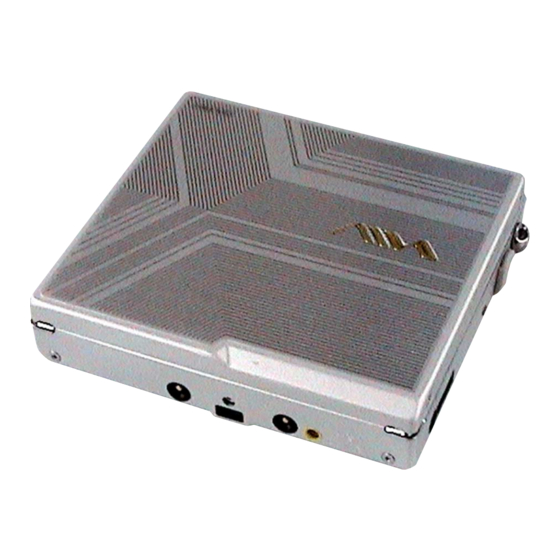
AM-NX1 SECTION 2 This section is extracted from instruction manual. GENERAL The recorder A Battery compartment B Terminals for attaching a battery charging stand C Terminals for attaching a dry battery case D DC IN 3V jack E OPEN switch F Handstrap hole Use the hole to attach your own strap. -
Page 6: Disassembly
AM-NX1 SECTION 3 DISASSEMBLY • This set can be disassembled in the order shown below. 3-1. DISASSEMBLY FLOW Note 1: The process described in can be performed in any order. Note 2: Without completing the process described in , the next process can not be performed. -
Page 7: Bottom (Ce) Panel Sub Assy
AM-NX1 Note: Follow the disassembly procedure in the numerical order given. 3-2. BOTTOM (CE) PANEL SUB ASSY 1 Slide to the direction of the arrow, open the battery case lid. 5 two screws (M1.4) 3 two screws (M1.4) 4 screws (M1.4) 6 bottom (CE) panel sub assy 2 battery case lid. -
Page 8: Upper Panel Sub Assy
AM-NX1 3-4. UPPER PANEL SUB ASSY 2 two screws 4 upper panel sub assy (M1.4) 3 two screws (M1.4) 1 Slide the knob (open) and open the upper panel sub assy. 3-5. ORNAMENTAL BELT ASSY 1 Pull to the direction of the arrow A 2 Open to the direction and remove two bosses B . -
Page 9: Mechanism Deck (Mt-Mzn910-181)
AM-NX1 3-6. MECHANISM DECK SECTION (MT-MZN910-181), CASE (BATTERY) BLOCK 1 two step screws (MD) 2 convex part 4 mechanism deck section (MT-MZN910-181) 8 spring (L) 3 convex part 0 set chassis assy 9 escutcheon (B) 5 four claws 7 spring (R) 6 case (battery) block 3-7. -
Page 10: Op Service Assy (Abx-1R)
AM-NX1 3-8. OP SERVICE ASSY (ABX-1R) 3 Remove lead screw block assy. 4 OP service assy (ABX-1R) 2 rack spring 1 precision pan screw (M1.4) (EG) 3-9. DC MOTOR SSM21A/C-NP (SLED) (M702), DC MOTOR SSM18D/C-NP (SPINDLE) (M701), DC MOTOR UNIT (OVER WRITE HEAD UP/DOWN) (M703) 3 two precision pan screws (M1.4) (EG) -
Page 11: Holder Assy
AM-NX1 3-10. HOLDER ASSY 4 Remove the holder assy to the direction of the arrow A . 2 boss 3 Open the holder assy. 1 boss... -
Page 12: Test Mode
AM-NX1 SECTION 4 TEST MODE Outline Operation in Setting the Test Mode • This set provides the Overall adjustment mode that allows CD • When the test mode becomes active, first the display check mode and MO discs to be automatically adjusted when in the test mode. - Page 13 AM-NX1 Configuration of Test Mode [VOL +] key: 100th place of item number [Major item switching] increase. [Test Mode $Display Check Mode%] [VOL --] key: 100th place of item number decrease. > [VOL +] Press the [VOL +] [Manual Mode]...
- Page 14 AM-NX1 5. The display changes a shown below each time the Overall Adjustment Mode [DISPLAY] key is pressed. Mode to adjust the servo automatically in all items. Normally, automatic adjustment is executed in this mode at the repair. • Address & Adjusted Value Display For further information, refer to “SECTION 5 ELECTRICAL...
- Page 15 AM-NX1 • Description of Error Indication Codes Problem Indication code Meaning of code Simple display Description No error No error No error Illegal access target Adrs Attempt to access an abnormal address address was specified Servo system error High temperature...
- Page 16 AM-NX1 Sound Skip Check Result Display Mode • Setting Method of Key Check Mode 1. Set the test mode (see page 12). This set can display the count of errors that occurred during the [DISPLAY] 2. Press the key for about 3 seconds activates the recording/playing for checking.
-
Page 17: Electrical Adjustments
• Test CD disc TDYS-1 3. Press the – key once more. (Part No. : 4-963-646-01) • SONY MO disc available on the market LCD display • Digital voltmeter • Laser power meter LPM-8001 R e s * * * (Part No. - Page 18 AM-NX1 Power Supply Manual Adjustment • Adjustment Method of VC1_HIGH (item number: 742) • Adjustment sequence Adjustment must be done with the following steps. LCD display 1. VC1_LOW adjustment (item number : 741) 2. VC1_HIGH adjustment (item number : 742) V C 1 H * * 3.
- Page 19 AM-NX1 • Adjustment Method of VC2_HIGH • Adjustment Method of REG2 (item number: 744) (item number: 746) LCD display LCD display V C 2 H i * * R E G 2 * * ** : adjusted value ** : adjusted value 1.
- Page 20 AM-NX1 • Adjustment Method of REG3_LOW (VC2_HIGH) • Adjustment Method of VREC_LOW (item number: 748) (item number: 751) LCD display LCD display R E G 3 L 2 * * V R E C L * * ** : adjusted value ** : adjusted value 1.
- Page 21 AM-NX1 • Adjustment Method of VREC_HIGH • Adjustment Method of ChgV_H (item number: 753) (item number: 756) LCD display LCD display V R E C H * * C h g V H * * ** : adjusted value ** : adjusted value 1.
- Page 22 AM-NX1 • Adjustment Method of ChgI_H Adjustment and Connection Location: (item number: 758) – MAIN Board (Component Side) – LCD display C I H ** : adjusted value TP602 (VREC) TP902 1. In the state of power off, short SL952 on the MAIN board (VC1) with a solder bridge.
- Page 23 AM-NX1 Power Supply Adjustment Auto Item Feed 5. Connect a digital voltmeter to the measuring points on the [VOL +] MAIN board, and adjust the voltage with the [VOL --] Note: This mode is available to perform the temperature correction and key.
- Page 24 AM-NX1 Laser Power Check Adjustment Required Before Overall Adjustment Note: If result of measurement of the laser power does not satisfy the Change the following adjustment value of two items before over- specification, either replace the OP (optical pick-up unit) or check all adjustment.
- Page 25 AM-NX1 • Overall Adjustment Mode (Title Display) 7. In case of MO overall adjustment NG, readjust from the NV reset (see page 17). The temperature correction (see page 17) LCD display may be omitted. A s s y * *...
- Page 26 AM-NX1 • CD and MO Overall Adjustment Items 2. MO overall adjustment items 1. CD overall adjustment items Item No. Description Item No. Description VC,VR power supply H/L selection VC,VR power supply H/L selection R_GRV setting . servo OFF HPIT setting . servo OFF...
- Page 27 AM-NX1 Remuse Clear Item No. Description Perform the Resume clear when all adjustments completed. Focus gain adjustment Tracking gain adjustment • Resume Clear Setting Method TWPP gain adjustment 1. Select the manual mode of the test mode, and set item number TWPP offset adjustment 1 043 (see page 13).
- Page 28 AM-NX1 Rewriting the Patch Data at Replacement of Main Board This set requires the patch data in the nonvolatile memory (IC851) to be rewritten using the application, when the MAIN board was replaced. Caution: The application that meets the microcomputer version in this set must be used when rewriting the patch data. Rewriting the patch data using the application not suitable for the microcomputer version could cause the set to malfunction.
- Page 29 AM-NX1 5. Confirm that the model and version indicated on the title bar coincide with the codes displayed in the Device Name block and the Version block in the window. 6. Click the [Write + Read] button. The patch data writing and the verify processing will be executed automatically in the following order:...
- Page 30 AM-NX1 • Confirmation of contents of the patch data rewrited 1. Click the [READ] button to confirm the contents of the patch data rewrited. 2. The application reads out the front and reverse patch areas and displays the results in the edit box.
- Page 31 AM-NX1 • Disconnecting the USB cable Disconnect the USB cable as the following procedure after rewriting the patch data and confirmation. Note: When the following procedure is not completed but USB cable is extracted, the application does not recognize the set at exchanging of the set.
- Page 32 AM-NX1 Rewriting the NV values Caution: The application that meets the microcomputer version in this set must be used when rewriting the NV values. Rewriting the NV values using the application not suitable for the microcomputer version could cause the set to malfunction.
- Page 33 AM-NX1 5. Confirm that the model and version indicated on the title bar coincide with the codes displayed in the Device Name block and the Version block in the window. 6. Click the [Write + Verify] button. The NV values writing and the verify processing will be executed automatically in the following order:...
- Page 34 AM-NX1 7. The operation will terminate with “Compere OK” given to all areas. If “Compere NG” is given to any area, the nonvolatile memory will be faulty. 8. Click the [USB DISCONNECT] button.
- Page 35 AM-NX1 9. Confirm that the window becomes as shown below where the [Write + Verify] button is inactive. 10. Disconnect the USB cable from the personal computer and the set. In the case of AEP, UK model, change the following adjustment value of two items after rewriting the NV values.
- Page 36 AM-NX1 MEMO...
-
Page 37: Diagrams
AM-NX1 SECTION 6 DIAGRAMS 6-1. BLOCK DIAGRAM – MAIN Section – OVER WRITE HEAD DRIVE IC601 (1/2) HR601 OVER WRITE OVER HEAD DRIVE OPTICAL PICK-UP BLOCK PRE DRIVER WRITE Q601, 602 (ABX-1R) HEAD (Page 38) VRECIN2 OUTA VRECO M703 H-BRIDGE... -
Page 38: Block Diagram - Power Supply Section
AM-NX1 6-2. BLOCK DIAGRAM – POWER SUPPLY Section – POWER CONTROL IC901 VB B+ (Page 37) VREF SDO0 DATA SDO0 SCK0 SCK0 DTC2 (Page 37) DTC1 VRMC RMC KEY (Page 37) XWAKE3 XWAKE4 FFCLR FFCLR SLEEP SLEEP D902 XCS PWR IC... -
Page 39: Note For Printed Wiring Board And Schematic Diagrams
AM-NX1 Ver 1.1 6-3. NOTE FOR PRINTED WIRING BOARD AND SCHEMATIC DIAGRAMS • Waveforms 1 IC501 9 (RFO) 6 IC801 ef (CLK) Note on Printed Wiring Board: Note on Schematic Diagram: • X : parts extracted from the component side. -
Page 40: Printed Wiring Board - Main Board (Component Side)
AM-NX1 6-4. PRINTED WIRING BOARD – MAIN Board (Component Side) – :Uses unleaded solder. • Semiconductor Location Ref. No. Location D602 D603 D901 D951 S804 PROTECT D952 DETECT D1001 D-10 D1002 D-10 IC501 IC701 IC721 Q601 Q602 CN952 (FRONT VIEW) -
Page 41: Printed Wiring Board - Main Board (Conductor Side)
AM-NX1 6-5. PRINTED WIRING BOARD – MAIN Board (Conductor Side) – :Uses unleaded solder. • Semiconductor Location Ref. No. Location D101 D201 MAIN BOARD (CONDUCTOR SIDE) D302 D381 M702 D604 (SLED) D653 D902 D904 M703 OVER WRITE HEAD UP/DOWN S801... -
Page 42: Schematic Diagram - Main Board (1/4)
AM-NX1 6-6. SCHEMATIC DIAGRAM – MAIN Board (1/4) – • • See page 39 for Waveforms. See page 46 for IC Block Diagrams. (1/4) CN501 TRK+ TRK+ FCS- FCS- FCS+ FCS+ TRK- TRK- LD-A L502 LD-K 10µH C513 MDVCC 0.022... - Page 43 AM-NX1 6-7. SCHEMATIC DIAGRAM – MAIN Board (2/4) – • See page 39 for Waveforms. (2/4) XRST RMC_KEY R835 4.7k L802 10µH R824 470k R821 R822 220k R872 R834 4.7k C837 C845 R856 1000p 0.022 R847 X802 S801 R857 C838...
- Page 44 AM-NX1 6-8. SCHEMATIC DIAGRAM – MAIN Board (3/4) – • • See page 39 for Waveform. See page 46 for IC Block Diagrams. (Page 42) (Page 43) (3/4) Q601 MCH6616 D602 D603 MA2YD1700LS0 MA2YD1700LS0 HR601 Q601,602 OVER WRITE OVER WRITE...
-
Page 45: Schematic Diagram - Main Board (2/4)
AM-NX1 Ver 1.1 6-9. SCHEMATIC DIAGRAM – MAIN Board (4/4) – • See page 46 for IC Block Diagrams. (Page 43) (4/4) R852 (NOT SUPPLIED) 100k IC851 TP902 AK6510CL C851 (VC1) XCS_NV SDI0 R853 XHOLD 100k SCK0 SDO0 R854 EEPROM... - Page 46 AM-NX1 • IC Block Diagrams IC381 AN17020A-VB IC601 XPC18A22AEPR2 BEEP VC2 VG OUTPUT SW CHARGE CHARGE MUTING PUMP 2 PUMP 1 OUTPUT SW VC VG DC IN HEADPHONE AMP CHARGE MONITOR HI-BRIDGE − VREF VREF CH1 OUT BATM X2/X4 PRE DRIVER...
- Page 47 AM-NX1 IC701 SC111258EPR2 42 41 35 34 31 30 29 PWM2 3PHASE CONTROL 3PHASE H-BRIDGE H-BRIDGE PRE DRIVER PRE DRIVER CONTROL VC LOW VOLTAGE DETECTOR COM2 CPUI2 – CPUO2 CPVO2 CPVI2 – CPWO2 CPWI2 – BIAS GND2 VC VG GND1 –...
- Page 48 AM-NX1 IC901 SC901580EPR2 (HP AMP) AMP1 CONTROL BANDGAP FFCLR1 48 VREF REFERENCE XWK4 47 REGC3 REF1 XWK3 46 REGC2 REF2 REF3 XWK2 45 REGC1 REF4 REF5 XWK1 44 REGI1 SERIES PASS REGULATOR1 REF3 VRMC 43 REGO1 FFCLR 42 VC2 SERIES PASS...
- Page 49 AM-NX1 IC951 SC901582EPR2 NSW4 VREF TIME CAP_C_LIM DIVIDER VI2DET PGND NSW3 LOGIC SIGNAL I_CTL1 RECEIVER NSW1 LOGIC I_SEL SIGNAL I_CTL2 RECEIVER AD_SEL WK_DET VREF PWR_WAKE DELAY VREF BATT VOLTAGE REFERENCE...
-
Page 50: Ic Pin Function Description
AM-NX1 6-10. IC PIN FUNCTION DESCRIPTION • IC501 SN761058AZQLR (RF AMP, FOCUS/TRACKING ERROR AMP) Pin No. Pin Name Description I-V converted RF signal (IX) input from the optical pickup detector 2, 3 PS, EQ — Connected to the external capacitor for the RF and EQ AGND —... - Page 51 AM-NX1 Pin No. Pin Name Description PEAK Peak hold signal output of the light amount signal (RF/ABCD) to the system controller Signal (D) input from the optical pickup detector Signal (A) input from the optical pickup detector Signal (B) input from the optical pickup detector...
- Page 52 AM-NX1 • IC801 CXD2680-207GA (SYSTEM CONTROLLER, DIGITAL SIGNAL PROCESSOR, 16M BIT D-RAM) Pin No. Description Pin Name OSCI Resonator connection terminal for the system clock (22.5792MHz) OSCO Resonator connection terminal for the system clock (22.5792MHz) Reference voltage (+1.1V) output terminal to the headphone amplifier (for the built-in...
- Page 53 AM-NX1 Pin No. Description Pin Name SLDW Sled motor drive control signal output (W) to the motor driver SLCU Sled motor drive comparison signal input (U) from the motor driver SLCV Sled motor drive comparison signal input (V) from the motor driver...
- Page 54 AM-NX1 Pin No. Description Pin Name XMUTE Analog muting control signal output to the headphone amplifier “L”: muting ON XPATCH Patch function detection terminal “L”: patch function (fixed at “L” in this set) Serial data input from the nonvolatile memory...
- Page 55 AM-NX1 Pin No. Description Pin Name XCS_NV Chip select signal output to the nonvolatile memory CHG_PWM Output voltage control signal output to the battery charge control VREC_PWM PWM signal output for the power supply voltage control to the REC driver...
- Page 56 AM-NX1 Pin No. Description Pin Name XHP_DET Headphone jack detection signal input Not used SET_CODE0 Input terminal for the set SET_CODE1 Input terminal for the set SET_CODE2 Input terminal for the set SET_CODE3 Input terminal for the set 195, 196...
- Page 57 AM-NX1 Pin No. Description Pin Name IFVSS2 — Ground terminal (for the microcomputer I/F block) IFVDD3 — Power supply terminal (+2.2V) (for the microcomputer I/F block) IFVSS3 — Ground terminal (for the microcomputer I/F block) IFVDD4 — Power supply terminal (+2.2V) (for the microcomputer I/F block) IFVSS4 —...
-
Page 58: Exploded Views
AM-NX1 Ver 1.1 SECTION 7 EXPLODED VIEWS NOTE: • -XX and -X mean standardized parts, so they • Items marked “*” are not stocked since they The components identified by mark 0 or dotted line with mark may have some difference from the original are seldom required for routine service. -
Page 59: Chassis Section
AM-NX1 Ver 1.1 7-2. CHASSIS SECTION mechanism deck section (MT-MZN910-181) supplied supplied main board supplied Ref. No. Part No. Description Remark Ref. No. Part No. Description Remark 3-246-521-02 BELT, ORNAMENTAL X-3382-650-1 TERMINAL (PLUS) ASSY, BATTERY 3-246-522-01 KNOB (OPEN) 3-246-497-02 TERMINAL BOARD (AA BATTERY) -
Page 60: Mechanism Deck Section (Mt-Mzn910-181)
AM-NX1 7-3. MECHANISM DECK SECTION (MT-MZN910-181) not supplied not supplied M702 not supplied M701 M703 The components identified by mark 0 or dotted line with mark 0 are critical for safety. Replace only with part number specified. Ref. No. Part No. -
Page 61: Electrical Parts List
AM-NX1 Ver 1.1 SECTION 8 ELECTRICAL PARTS LIST MAIN NOTE: • Due to standardization, replacements in the • Items marked “*” are not stocked since they The components identified by mark 0 or dotted line with mark parts list may be different from the parts speci- are seldom required for routine service. - Page 62 AM-NX1 MAIN Ref. No. Part No. Description Remark Ref. No. Part No. Description Remark C902 1-137-858-11 TANTALUM CHIP 47uF 6.3V C701 1-119-923-11 CERAMIC CHIP 0.047uF C903 1-137-858-11 TANTALUM CHIP 47uF 6.3V C702 1-164-943-11 CERAMIC CHIP 0.01uF C904 1-137-858-11 TANTALUM CHIP 47uF 6.3V...
- Page 63 AM-NX1 Ver 1.1 MAIN Ref. No. Part No. Description Remark Ref. No. Part No. Description Remark Q608 8-729-053-71 FET TS8K1TB D603 8-719-081-35 DIODE MA2YD1700LS0 Q651 8-729-047-48 TRANSISTOR UMD12N-TR D604 6-500-483-01 DIODE MA22D2800LS0 Q652 8-729-046-45 FET SI2302DS-T1 D653 6-500-483-01 DIODE MA22D2800LS0...
- Page 64 AM-NX1 MAIN Ref. No. Part No. Description Remark Ref. No. Part No. Description Remark R656 1-218-985-11 RES-CHIP 470K 1/16W R847 1-218-965-11 RES-CHIP 1/16W R848 1-218-953-11 RES-CHIP 1/16W R658 1-218-961-11 RES-CHIP 4.7K 1/16W R849 1-218-957-11 RES-CHIP 2.2K 1/16W R659 1-218-957-11 RES-CHIP 2.2K...
- Page 65 AM-NX1 Ver 1.1 MAIN Ref. No. Part No. Description Remark Ref. No. Part No. Description Remark < COMPOSITION CIRCUIT BLOCK > AC power adaptor (1) RB701 1-233-963-21 RES, NETWORK (CHIP TYPE) 2.2K RB702 1-233-967-11 RES, NETWORK (CHIP TYPE) 10K < SWITCH >...
- Page 66 AM-NX1 REVISION HISTORY Clicking the version allows you to jump to the revised page. Also, clicking the version at the upper right on the revised page allows you to jump to the next revised page. Ver. Date Description of Revision 2003.07...