Advertisement
Quick Links
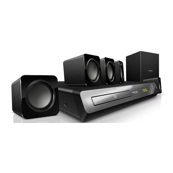
Home Theater DVD Player
Service
TABLE OF CONTENTS
Location of PCB Boards & version variation & repair scenario matrix..................... 1-2
Production Specifications ...............................................................................................1-3
Safety Instruction, Warning & Notes................................................................................1-
D
Instruction................................................................................................................2-1
FU
Mechanical and Dismantling Instructions ........................................................................3-1
Software Upgrades........................................................................................................... -1
Trouble Shooting Chart .................................................................................................... -1
Wiring Diagrams ................................................................................................6-1
Electrical Diagrams and Print-layouts .................................................................7-1
Set Mechanical Exploded view ....................................................................................... -1
Revision List ...................................................................................................................
©
Copyright 2010 Philips Consumer Electronics B.V. Eindhoven, The Netherlands
All rights reserved. No part of this publication may be reproduced, stored in a retrieval system or
transmitted, in any form or by any means, electronic, mechanical, photocopying, or otherwise without
the prior permission of Philips.
Published by Helen-RY 1216 Service Audio Printed in The Netherlands Subject to modification
Version 1.0
Version 1.0
Version 0.0
HTS2512/94
Page
7
4
5
8
-1
9
CLASS 1
LASER PRODUCT
©
313978536220
GB
GB
Advertisement

Related Manuals for Philips HTS2512/94


Summary of Contents for Philips HTS2512/94
- Page 1 LASER PRODUCT © Copyright 2010 Philips Consumer Electronics B.V. Eindhoven, The Netherlands All rights reserved. No part of this publication may be reproduced, stored in a retrieval system or transmitted, in any form or by any means, electronic, mechanical, photocopying, or otherwise without the prior permission of Philips.
- Page 2 PCB BOARD LOCATION: AV BOARD MAIN BOARD POWER BOARD LOADER Version Variation Type/Versions HTS2512 Features Power supply rating:220-240V ,50Hz Power consumption:55W Repair Scenario Matrix Type/Versions HTS2512 Board in used Main Board Front Control Board Amplifier Board Power Board *Bd:Board Level Replacement *C:Component Level Repair...
- Page 3 HTS2512/94 Product Specifications Video Note • Signal system: PAL / NTSC • Component video output: 480i/576i, • Specifi cations and design are subject to change without notice. 480p/576p, 720p, 1080i Audio Region codes • S/PDIF Digital audio input: • Coaxial: IEC 60958-3 The type plate on the back or bottom of the •...
- Page 4 Subwoofer • Output power: 50 W RMS (30% THD) • Impedance: 8 ohm • Speaker drivers: 133 mm (5.25") woofer • Dimensions (WxHxD): 195 x 265 x 265 mm • Weight: Speakers Center speaker: • Output power: 50 W RMS (30% THD) •...
- Page 5 Safety instruction, Warning & Notes Safety instruction 1. General safety 2.Laser safety Safety regulations require that during a repair: This unit employs a laser. Only qualified service personnel . Connect the unit to the mains via an isolation transformer. may remove the cover, or attempt to service this device .
- Page 6 Warning 1.General 2. Laser . All ICs and many other semiconductors are susceptible to . The use of optical instruments with this product, will electrostatic discharges (ESD). Careless handing during increase eye hazard. repair can reduce life drastically. Make sure that, during .
- Page 7 Solder Joint...
- Page 8 - lead free BGA-ICs will be delivered in so-called respected by the workshop during a repair: ‘dry-packaging’ (sealed pack including a silica gel Use only lead-free solder alloy Philips SAC305 with pack) to protect the IC against moisture. After order code 0622 149 00106. If lead-free solder-paste is...
- Page 9 EN Before using your product, read all accompanying safety NL Lees voordat u het product gaat gebruiken eerst alle information bijbehorende veiligheidsinformatie CS P ed použitím produktu si p e t te doprovodné NO Lees voordat u het product gaat gebruiken eerst alle bezpe nostní...
- Page 10 EN Connect the home theater NL Sluit de home cinema aan CS P ipojte domácí kino NO Koble til hjemmekinoanlegget DA Tilslut hjemmebiografen PL Pod czanie zestawu kina domowego DE Anschließen des Home PT Efectuar as ligações ao sistema de cinema em casa Entertainment-Systems RO Conecta i sistemul home theater home cinema...
- Page 11 EN Connect to TV in one of these ways IT Esegui il collegamento al TV in uno dei modi indicati di seguito CS P ipojení k televizoru prove te jedním z následujících NL Maak op een van de volgende manieren verbinding met zp sob de TV DA Tilslut til TV på...
- Page 12 VIDEO + AUDIO L/R AUDIO L/R AUDIO IN VIDEO OUT AUDIO OUT VIDEO IN...
- Page 13 EN Switch on the home theater NL Schakel de home cinema in CS Zapn te domácí kino NO Slå på hjemmekinoanlegget DA Tænd for hjemmebiografen PL W czanie zestawu kina domowego DE Einschalten des Home PT Ligar o sistema de cinema em casa Entertainment-Systems RO Porni i sistemul home theater home cinema...
- Page 14 EN Complete the fi rst time setup NL Voltooi de eerste installatie CS Dokon ili jste nastavení p i prvním zapnutí NO Fullføre den første konfi gureringen DA Fuldfør den indledende opsætning PL Pierwsza konfi guracja DE Abschließen der Ersteinrichtung PT Executar a confi...
- Page 15 EN Use your home theater IT Utilizzo del sistema Home Theater CS Použití domácího kina NL Uw home cinema bedienen DA Brug af din hjemmebiograf NO Bruke hjemmekinoanlegget DE Verwenden des Home PL Korzystanie z zestawu kina domowego Entertainment-Systems PT Utilizar o sistema de cinema em casa home cinema RO Utiliza i sistemul home theater ES Uso del sistema de cine en casa...
- Page 17 Your home theater Remote control Congratulations on your purchase, and welcome This section includes an overview of the remote to Philips! To fully benefi t from the support that control. Philips offers, register your product at www.philips.com/welcome. Main unit This section includes an overview of the main unit.
- Page 18 2-10 REPEAT / PROGRAM ( Standby-On ) • Select or turn off repeat mode. Switch the home theater on or to standby. • In radio mode, press once to access ( Home) program mode, and press again to store Access the home menu. the radio station.
- Page 19 Mechanical and Dismantling Instructions Dismantling Instruction Detailed information please refer to the model set. The following guidelines show how to dismantle the player. Step1: Remove 6 screws around the Top Cover, and then remove the Top Cover (Figure 1). Figure 1 Step2: If it is necessary to dismantle Loader or Front Panel, the Front door should be removed first.
- Page 20 Mechanical and Dismantling Instructions Detailed information please refer to the model set. Dismantling Instruction :Dismantle Front Panel, disconnect the connectors (XP22, XP33), need release 2 snaps of Front Panel & 2 snaps Step3 of bottom cabinet , then gently pull the Panel out from the set. (Figure 3) Figure 3 Step4 : Dismantle Front Control Board,remove 5 screws (Figure 4...
- Page 21 Mechanical and Dismantling Instructions Dismantling Instruction Detailed information please refer to the model set. : Dismantle Main Board, first disconnect 1 connector (XP36), and then remove 7 screws. (Figure 5/6) Step6 : Dismantle Power Board, disconnect the connector s XP3 and XS703 ,then remove 5 screws.(Figure 5/6) Step7 (Figure 5/6) Step8: Dismantle AV Board, first disconnect 1 connector(XP11),and then remove...
- Page 22 Caution: The set must not be power off during upgrading, Otherwise the Main board will be damaged entirely. How to adjust the setting after repairing: 1.HTS2512/94: Open DVD tray, press “9” “9” “9” “9” “5” on R/C; Note: Restart after above steps.
- Page 23 Trouble shooting Chart LED No display on Front Control Board LED No display on Front Control Board Check every supply voltage on Main Board whether normal or not. Refer to CN502 on Power Board (XP33 PIN3:+12V, PIN5&6: +5V) Check voltage +5V, +12V on Power Board Fix the connection XP3 on Front at CN502 position and Front Control Board Control Board...
- Page 24 Trouble shooting Chart keys do not work keys do not work Fix the connection XP3 on Front Control Check voltage +5V on Front Control Board Board and XP33 on MAIN BOARD (XP3 PIN14) and voltage +5V on U301 PIN7 Check Front Control Board signals (U301 Replace U301 on Front Control PIN5,PIN6) Board...
- Page 25 Trouble shooting Chart Remote control does not work Remote control does not work Check battery of remote control whether Replace the battery for remote exhausted or not. control Check power supply of IR601 on Front Check the +3.3V net on Front Control Board whether normal or not Control Board XP3 XP3 PIN8 3.3V...
- Page 26 Trouble shooting Chart No audio output No audio output Check XP502 pin 2&3 34V on Power Check voltage +34V whether normal or not Board whether normal or not at XS703 on Amplifier Board Power Board Replace Check the control signal whether right or Replace main Board not at theXP3 PIN7 +2.4V on Main Board Replace Amplifier Board...
- Page 27 Trouble shooting Chart No video output No video output Check L9 , R555 whether right on Main Change L9, R555 on Main Board Board Check the video signal whether right at U1: PIN69 Change U1 and Replace Main Board...
- Page 28 Trouble shooting Chart Can’t read disc or can’t open the disk door Can’t read disc or can’t open the disk door Check loader whether work normally Check XP2 on Main Board or not Check 24pin 6pin and 5pin cable from Main Board to Loader whether Fix 24pin 6pin and 5pin cable connect right or not Replace Loader...
- Page 29 Trouble shooting Chart Tuner FM does not work Tuner FM does not work Check voltage U183 PIN6&9:+3.3V Main Board Check Main Board tuner power supply whether normal or not circuit. Check voltage +3.3V at Tuner module (TUN1 pin5) whether right or Check Main Board tuner power supply circuit.
- Page 30 Trouble shooting Chart AUX in does not work AUX in does not work Check voltage at XP3 PIN3:12V on Main Board whether normal or not Refer to Power Board CN502 Check Main Board U6 PIN2,PIN15 signal Check C166,C167,R87,R91 input whether right or not Check voltage at U6 PIN3&13 on Check Main Board U6 power supply and out Main Board Whether normal or not...
- Page 31 Trouble shooting Chart OPTICAL IN does not work OPTICAL in does not work Check voltage at P4 PIN1:3.3V on Main Board whether normal or not Refer to Power Board CN502 Check Main Board P4 PIN3 signal input whether right or not Check Main Board C108, Check voltage at U707 PIN5:3.3V on Main Refer to Power Board CN502...
- Page 32 HTS2512/94 Block /Wiring Diagram: 8ohm 4ohm 4ohm 4ohm 4ohm 4ohm SUB+ CEN+ AUX IN CVBS OPTI IN COAX IN YUV OUT SUB- CEN- 74HC04 TS1G3157 SCART8 74HC4052 AS4558 AK5358 POWER SCART16 DERATING CVBS_O TUNER IIC M052_54 CONTROL STA518 STA518 HOMESW...
- Page 33 14PIN/1.0mm 14PIN/1.0mm Front Control Board Circuit Diagram: +12V R637 R637 VSCLK R641 R641 VSDA R639 R639 VSTB KEY_POW MP3_L MO_5V MP3_R R316 R316 NC/33 NC/33 LED- R694 R694 R703 R703 R704 R704 R705 R705 4.7K 4.7K 4.7K 4.7K 4.7K 4.7K U301 U301 GRID[1:7]...
- Page 34 R540A R540A CY506 CY506 XP502 4PIN/2.5mm XP502 4PIN/2.5mm C533 C533 1500pF/1KV 1500pF/1KV R575 R575 Q571 Q571 Power Board Circuit Diagram: R540B R540B 470pF/250VAC 470pF/250VAC PNP_MMBT8550CLT1 PNP_MMBT8550CLT1 M+5V R540C R540C T531 T531 PQ3230 PQ3230 R578 R578 Alternative L531 L531 T531P +33V CN531 CN531 6PIN/2.5mm/70mm...
- Page 35 Main Board Circuit Diagram: Power Supply +12V: +12V(+-10%) +5Vin +5V: +5V(+-2.5%) POWER_control POWER_c MO_VCC TO POWER BOARD 300/2A 300/2A ASM3403M ASM3403M 12-SM3403-0BX 1uF/50V/Y5V 1uF/50V/Y5V 4.7K 4.7K 0.1uF/25V/Y5V 0.1uF/25V/Y5V 100uF/10V 100uF/10V 0603 8PIN/2.5mm 8PIN/2.5mm C125 C125 0.1uF/25V/Y5V 0.1uF/25V/Y5V A+5V MO_VCC U706 U706 R819 R819...
- Page 36 Main Board Circuit Diagram: SPHE8202RQ-D DV33 FV33 CVBS FB40 FB40 500/200mA 500/200mA CVBS 4.7K 4.7K MO_VCC XP21 XP21 VVCC3 27MHz/30PPM 27MHz/30PPM U176 U176 RF3.3V SF_CS 33pF/50V/NP0 33pF/50V/NP0 33pF/50V/NP0 33pF/50V/NP0 SPI_D0 VCC1.2 DVCC3 DVCC3 HOLD# SF_CK 4PIN/2.0mm 4PIN/2.0mm R195 R195 VCC1.2 C257 C257 SPI_D1...
- Page 37 Main Board Circuit Diagram: SDRAM & USB SD33 MA10 DQ10 A10/AP DQ10 MA11 DQ11 DQ11 DBA0 DQ12 BA0/A13 DQ12 DBA1 DQ13 BA1/A12 DQ13 DQ14 DQ14 SDCLK DQ15 DRAS# RAS# DQ[0..15] DQ15 DQ[0..15] SD33 SD33 DWE# MA[0..11] MA[0..11] BA[0..1] BA[0..1] DRAS# DCAS# CAS# DQM[0..1]...
- Page 38 Main Board Circuit Diagram: AUDIO_IN TUNER_L +6VA TUNER_L R167 1M R167 1M TUNER_R TUNER_R R166 1M R166 1M +6VA R164 NC/1M R164 NC/1M AL_CH3 1uF/16V/Y5V 1uF/16V/Y5V 1uF/16V/Y5V 1uF/16V/Y5V CE46 CE46 R165 NC/1M R165 NC/1M TUNER_L C163 C163 AL_CH2 AUX_L C166 C166 AL_CH3 AR_CH3...
- Page 39 Main Board Circuit Diagram: Video Out V+5V NC/RCA/3h NC/RCA/3h R548 R548 C101 C101 NC/33 NC/33 100pF/50V/NP0 100pF/50V/NP0 10pF/50V/NP0/NC 10pF/50V/NP0/NC V+5V CVBS_O CVBS_O CVBS 1.2uH/25mA 1.2uH/25mA CE18 47uF/10V CE18 47uF/10V R549 R549 AVCC CVBS NC/NPN_3DG3904M NC/NPN_3DG3904M C103 C103 100pF/50V/NP0 100pF/50V/NP0 0.1uF/25V/Y5V 0.1uF/25V/Y5V VIDEO I/F R555...
- Page 40 Main Board Circuit Diagram: MCU & CONNECTOR +3.3V_STB R425 R425 R559 R559 +3.3V_STB +3.3V_STB NC/4.7K NC/4.7K 12MHz/30PPM 12MHz/30PPM MCU_SCL MCU_RST MCU_SDA R106 R106 20pF/50V/NP0 20pF/50V/NP0 20pF/50V/NP0 20pF/50V/NP0 NC/EEPROM_16Kb_AF24BC16 NC/EEPROM_16Kb_AF24BC16 SOP8-244-1.27 SOP8-244-1.27 MCU_RST +3.3V_STB XP33 XP33 CE255 CE255 +3.3V_STB SPI_CS MIC_LR MIC_LR 10uF/10V 10uF/10V...
- Page 41 Main Board Circuit Diagram: STA309A VD3.3V D705 D705 Q702 Q702 LL4148 LL4148 PNP_MMBT8550CLT1 PNP_MMBT8550CLT1 VD3.3V R739 R739 C716 C716 0.1uF/25V/Y5V 0.1uF/25V/Y5V CE723 CE723 100uF/10V 100uF/10V AMP_MUTE R805 R805 4.7K 4.7K Q701 Q701 C714 C714 C715 C715 NPN_3DG3904M NPN_3DG3904M VD3.3V EAPD 0.1uF/25V/Y5V 0.1uF/25V/Y5V 0.1uF/25V/Y5V...
- Page 42 7-10 7-10 Main Board Circuit Diagram: STA518 U701 U701 VCC-Sign SUB-GND SUB- TP26 TP26 L702 L702 22uH/3.3A 22uH/3.3A TP27 TP27 SUB+ VCC-Sign OUT2B C734 C734 C735 C735 TP28 TP28 C454 C454 0.1uF/50V/X7R 0.1uF/50V/X7R 0.1uF/50V/X7R 0.1uF/50V/X7R 1uF//50V/X7R 1uF//50V/X7R TP29 TP29 OUT2B 0.1uF/50V/X7R 0.1uF/50V/X7R C452...
- Page 43 7-11 7-11 Front Control Board Print-layout (Bottom Side):...
- Page 44 7-12 7-12 Power Supply Print-layout (Bottom Side):...
- Page 45 7-13 7-13 Main Board Print-layout (Top Side):...
- Page 46 7-14 7-14 Main Board Print-layout (Bottom Side):...
- Page 47 Exploded View for HTS2512/94:...
- Page 48 REVISION LIST Version 1.0 * Initial release for HTS2512/94...