Table of Contents
Advertisement
Quick Links
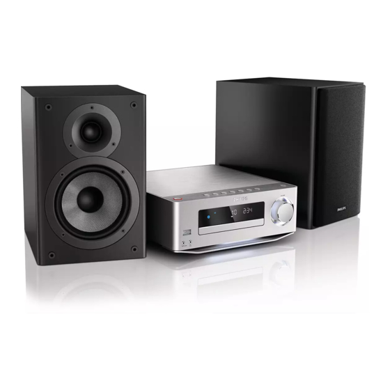
Micro System
C
o
n
e t
n
s t
...................................................1-1 to 1-9
2 Laser Beam Safety Precautions......................................... 2-1
3 Important Safety Precautions .................................. 3-1 to 3-2
4 Safety Check After Servicing ............................................. 4-1
Requirements .................................................................... 5-1
7 Direction of Use ....................................................... 7-1 to 7-3
8 Cabinet Disassembly Instructions ........................... 8-1 to 8-2
9 Troubleshooting ....................................................... 9-1 to 9-2
10 Block Diagram .................................................................10-1
11 Wiring Diagram ...............................................................11-1
Circuit Diagram ....................................................12-1
Layout Diagram ...................................................12-2
13 Display Board
Circuit Diagram ................................................12-3
Layout Diagram ...............................................12-4
© Copyright 2011 Philips Consumer Electronics B.V. Eindhoven, The Netherlands.
All rights reserved. No part of this publication may be reproduced, stored in a
retrieval system or transmitted, in any form or by any means, electronic,
mechanical, photocopying, or otherwise without the prior permission of Philips.
Published by Sophie-KM 1114 AVM
Version 1.0
P
a
g
e
Contents
14 Headphone & MP3 Link and USB、LED Board
15 Key Board
16 Power Board
17 Decoder Board
18 Exploded View....................................................................13-1
19 Revision List .......................................................................14-1
Printed in the Netherlands
MCM7000/12
Circuit Diagram .................................................12-5
Layout Diagram.................................................12-5
Circuit Diagram .................................................12-6
Layout Diagram ................................................12-7
Circuit Diagram ........................................12-8 to 12-9
Layout Diagram ..............................................12-10
Circuit Diagram .................................12-11 to 12-13
Layout Diagram ..............................................12-14
Feature
Different
Features
RDS
Voltage Selector
ECO Standby
DTS
Subject to modi cation
Page
/12
EN
Advertisement
Table of Contents

Related Manuals for Philips MCM7000/12


Summary of Contents for Philips MCM7000/12
-
Page 1: Table Of Contents
Feature Different Features © Copyright 2011 Philips Consumer Electronics B.V. Eindhoven, The Netherlands. All rights reserved. No part of this publication may be reproduced, stored in a Voltage Selector retrieval system or transmitted, in any form or by any means, electronic, ECO Standby mechanical, photocopying, or otherwise without the prior permission of Philips. -
Page 2: Technical Specification And Connection Facilities
Technical Specification and Connection Facilities Location of PC Boards Decoder Board AMP Board DVD Loader Key Board USB Board Power Board Headphone/MP3 Link Board LED Board Display Board Version Variations Type /Versions: MCM7000 Service policy Board in used: LED Board Decoder Board Display Board AMP Board... - Page 3 Technical Specification and Connection Facilities Technical Specification 1. General Information and Requirement Product Family Features 1.1.1 Identity and Key Features MCM7000 series are Heritage Range Micro Audio System CD/MP3 player with USB and Tuner FM(20presets) Elements to include as generic requirements: 1.
- Page 4 Technical Specification and Connection Facilities 2.1.3 External I/O Connections MCM7000 Model Stroke Version MP3 Link (3.5mm audio jack) Aux In (RCA cinch) Tuner Socket (for FM) Headphone Out (3.5mm audio jack) 2.1.4 Controls, Local Display and LED Indications(tbc) Control keys on the set are: Model MCM7000 Standby...
- Page 5 Technical Specification and Connection Facilities 2.1.5. ACCESSORIES (tbc) Model MCM7000 Stroke Version Power Cord 1.8M AV cable 1.5M Audio cable 0.5M (3.5mm audio) Tuner Antenna 1.5M 75ohm Speaker cable USB cable Remote Control 44keys Battery AAAx2 Quickly guide 3.Mechanical General Information The product appearances and functions are defined in their respective MUS.Product management approves the MUS and it is a leading document where product appearance is applicable.
- Page 6 Technical Specification and Connection Facilities 3.3.ESD Requirements The product shall withstand electro static discharges on all user accessible parts of the product. Reference: IEC61000-4-2. For contact discharges: General(kV) USA(kV) Requirement Level No deviations allowed. >2-4 >3-4 Short perceptible deviations allowed Normal recallable functions functon changes allowed.
- Page 7 Technical Specification and Connection Facilities 4. Technical Specifications Power Supply 4.1.1 Type and versions Build-inSMPS will be used for all models and stroke versions. All using figure '8' socket, will cater for all versions: Versions Region/Country SMPS Detachable mains cords EUROPE/UK 1) 100 ~240Vac nom.
- Page 8 Technical Specification and Connection Facilities 4.1.3 Mains Drop-out Immunity The product shall withstand mains failures of: Variation 0% (=100% dip) at T-event = 50 mSec. Performance criterion B Variation 40% (=60% dip) at T-event = 100 mSec. Performance criterion B Variation 0% (=100% dip) at T-event = 5 Sec.
- Page 9 Technical Specification and Connection Facilities Output Stage Protection: Temperature : Short Circuit: v i t Electrical Data ± --- Vol -20dB) 150nW i n i < Signal to Noise Ratio(A-weighted): 82dB : k l 55dB Audio Inputputs ± Audio Output(*1) Audio Input Sensitivity( 3dB) rated output power at 1kHz Tuner FM 67.5kHz, Modulation (Limit:-6dB)
- Page 10 Technical Specification and Connection Facilities 5.TUNER FM use Silicon Lab Si4704/4705(w/RDS) GENARAL PART WAVE RANGE VERSION TOLERANCE TUNING GRID FM 87.5 – 108.00 MHz /05/12 QUARTZ PRECISION 50kHz AERIAL : PIG TAIL ANT WIR ELECTRICAL DATA v i t y t i Search time digital tuning system.
-
Page 11: Laser Beam Safety Precautions
Laser Beam Safety Precautions This Blu-Ray player uses a pickup that emits a laser beam. Do not look directly at the laser beam coming from the pickup or allow it to strike against your skin. The laser beam is emitted from the location shown in the figure. When checking the laser diode, be sure to keep your eyes at least 30 cm away from the pickup lens when the diode is turned on. -
Page 12: Important Safety Precautions
Do not insert warped or cracked discs into the disc compartment. the combined weight of the product and the wall mount. Koninklijke Philips Remove discs from the disc compartment if you are not using the product for an Electronics N.V. bears no responsibility extended period of time. - Page 13 Important Safety Precautions Disposal of your old product and batteries Your product is designed and manufactured with high quality materials and components, which can be recycled and reused. When this crossed-out wheeled bin symbol is attached to a product it means that the product is covered by the European Directive 2002/96/EC.
-
Page 14: Safety Check After Servicing
Safety Check after Servicing Examine the area surrounding the repaired location for damage or deterioration. Observe that screws, parts, and wires have been returned to their original positions. Afterwards, do the following tests and confirm the specified values to verify compliance with safety standards. 1. -
Page 15: Safety Information General Notes & Lead Free Requirements
Safety Information, General Notes & Lead Free Requirements Safety Instructions Warnings General Safety General Safety regulations require that during a repair: All ICs and many other semiconductors are susceptible to Connect the unit to the mains via an isolation transformer. electrostatic discharges (ESD, ). -
Page 16: Standard Notes For Servicing,Lead Free Requirements & Handling Flat Pack Ic
1. The output pin of the 3 pin Regulator ICs is When soldering, be sure to use the Pb free solder. indicated as shown. Information about lead-free soldering Top View Philips CE is producing lead-free sets from 1.1.2005 Bottom View onwards. Input IDENTIFICATION Regardless of special logo (not always 2. - Page 17 2004), containing leaded solder-alloy and components, all needed spare-parts will be available till the end of the service-period. For repair of such sets nothing changes. On our website www.atyourservice.ce.Philips.com you find more Fig. S-1-1 information to: BGA-de-/soldering (+ baking instructions) 2.
- Page 18 Standard Notes for Servicing, Lead Free Requirements & Handling Flat Pack IC 3. The flat pack-IC on the CBA is affixed with glue, so 4. Release the flat pack-IC from the CBA using be careful not to break or damage the foil of each tweezers.
- Page 19 Standard Notes for Servicing, Lead Free Requirements & Handling Flat Pack IC Instructions for Handling Semi- 2. Installation conductors 1. Using desoldering braid, remove the solder from the foil of each pin of the flat pack-IC on the CBA Electrostatic breakdown of the semi-conductors may so you can install a replacement flat pack-IC more occur due to a potential difference caused by easily.
-
Page 20: Direction Of Use
The following excerpt of the DFU/QSG serves as an introduction to the set. The Complete Direction for Use can be download in different languages from the internet site of Philips Customer care Center : www.support.philips.com Overview of the main unit Overview of the main unit Headphone socket. - Page 21 Always follow the instructions in this chapter in Stop play. sequence. Erase a program. If you contact Philips, you will be asked for the (In standby mode) Turn on/off Demo model and serial number of this apparatus.The mode. model number and serial number are on the back of the apparatus.Write the numbers here:...
- Page 22 Direction of Use For the speaker side: Unscrew the speaker connectors. For the left speaker, identify the speaker cable that is connected to the left connectors on the main unit. LINE OUT AU X IN DEMO ANTENN A Insert fully the red end of the speaker cable into the red (+) connector.
-
Page 23: Cabinet Disassembly Instructions
Cabinet Disassembly Instructions Note: 1. Disassembly Flowchart (1) Identification (location) No. of parts in the figures This flowchart indicates the disassembly steps to gain (2) Name of the part access to item(s) to be serviced. When reassembling, (3) Figure Number for reference follow the steps in reverse order. - Page 24 Cabinet Disassembly Instructions A010 Fig. D3 Fig. D6 Fig. D4 Fig. D7 A011 A012 Fig. D5 Fig. D8...
-
Page 25: Troubleshooting
Troubleshooting FLOW CHART NO.1 NO Power(The power cannot be turned on) Check the Power Cable connect is ok or not Check and Change the connect cable TEST Power supply voltage output CON4 each TEST CON4 “ECO”pin whether plate is normal or not(+12V\DC5V\MCU\5V\P25V) has high level signal Check the fuse which location F1 replace a new one... - Page 26 Troubleshooting FLOW CHART NO.3 VFD no display Check VFD display board CN301 whether connection to decoder board CN1 is normal Check VFD display board CN401 whether Test whether VFD board CN401 pin 12#~13# between connection to KEYS board CN301 is normal has AC5V provide voltage Check the KEYS board location Check whether VFD board U401 pin 14#\33#\45# has +V5 B301 related electric circuit...
-
Page 27: Block Diagram
Block Diagram M3.3V M1.8V SONY pick up DM-06BXLX-L2 DVD Loader Main chipset Loader motor driver CD5888CB(1.18V) 23.7K 1% resistor Power Switch 5V 1A TPS2552DBVT ZR36966XE2 USB2 FRONT 12V /1A (11.7V-12.3V) 5V 2.5A IPHONE 28V 6A ESD REJECTOR 28V 6A MCU5V/1A 5V 3.5A M3.3V 6P/2.5... -
Page 28: Wiring Diagram
Wiring Diagram SPEAKER SPEAKER MBOY SPEAKER 2.0/2P SPKL+ SPKL- SPKR+ SPKR- 2.5/2P CVBS COAXIAL HDMI LINE OUT AUX OPTICAL 7.9/2P DIN9 4705 IP 5V TS5V330CDBQR 2.0/2P IP GND 2.5/4P 2.0/8P Power Board 1389G SDRAM FFC 1.0/16P Decoder Board SSCL MUTE 1117-1.2V 2.0/4P FFC 0.5/24P... - Page 29 AMP Board -- Circuit Diagram FM_ C P_R ST D AB_M U TE R 19 3 N C /33 0 ipo d/D AB_T X R 16 9 R 17 0 FB6 00 ipo d/D AB_R X N C /0 P25 V +1 2V R 19 4 N C /33 0 /RST...
- Page 30 AMP BOARD -- Layout Diagram 12-2 12-2...
- Page 31 Display Board -- Circuit Diagram 35-MBD7020-04A1 VFD BOARD V+5V -27V V+5V V+5V VFD401 HL-D1586 L401 NC/601 R417 0.47 R431 0.47 VF1 Q401 Q402 Q403 NC/9014 NC/9014 NC/9014 R416 0.47 C402 R430 0.47 S2-2 S3-3 S1-1 10KOhm/104 C403 R406 R408 R404 NC/104 R413 0/NC...
- Page 32 Display Board -- Layout Diagram 12-4 12-4...
- Page 33 Headphone & MP3 Link and USB、LED BOARD -- Circuit and Layout Diagram CN701 2.0/2P LED-LG-1 L+5V PHONE & MP3LINK BOARD USB BOARD J501 LED701 WHITE LED L503 MUTE-HP LED-LG-1 R701 220 L+5V L501 100uH L504 OUT L-HP L502 100uH L505 OUT R-HP L506 HP MUTE...
- Page 34 Key Board -- Circuit Diagram KEYS BOARD KEYS SCAN L326 200UH C301 CE301 B301 47uF/16V Q301 VF2~ C304 D965 473M VF1~ R302 5K6 SW306 R307 10 SW304 SW305 -27V SK3-1 R303 5K6 D302 SK2-1 FR104 SK1-1 Q302 K3-1 CE302 D965 K2-1 DZ301 220U/35V...
- Page 35 Key Board -- Layout Diagram 12-7 12-7...
- Page 36 Power Board -- Circuit Diagram 1 222M/400V Lp=0.48mH UU1.5-30mH T18*10*7mm 20mH 471M/400V +17.5V/3.5A 10uH/0.6mm 10A/150V 4*RL257 120K/1W 33uF/400V 33uF/400V 472/630V 102/1KV R18/19/20/R21 1500uF/25V 680uF/25V 680uF/25V 104/50V/1206 4X120R/1206 471M/400V 102/500V/1206 R30/R31 47R/1206*2 KA78L12 T5AH 250V Vout +12V/0.5A 10uH/0.6mm D10/D9 104/50V/1206 FR107 CE13 FR157 2*SF34...
- Page 37 Power Board -- Circuit Diagram 2 TO-6026 APM4800 SOP-8 +9-16Vdc AF 9435P PIN1,2,3 PIN5,6,7,8 80uH/0.7mm PIN4 +17.5V +20V/4A +17.5V 2*0.3R/1206 1000uF/10V 9.1K/0805 104/25V/1206 SB560 1K/0805 +12V/0.5A 6.2V/0.5W D+5V/1.5A 10K/0805 MCU5V C945 SOT-23 CON2 9P/2.5 471pF/50V MC 34063 A733 SOT-23 12-9 12-9...
- Page 38 Power Board -- Layout Diagram T5AH 250V 12-10 12-10...
- Page 39 Decoder Board -- Circuit Diagram 1 VDDPWM VDDAFE FB1 MBW2012-221 DR VSB DR VSB 10nF R1 75R 22pF OSCOUT HOMESW HOMESW FB2 MBW2012-221 VDDAFE DSPVCC33 27.000MHz 220K 10nF 10nF OSCIN 22pF 100uF/10V FB3 MBW2012-221 VDDDAC DSPVCC33 FOCUS_PWM TRACK_PWM 33pF SPDL_PWM 10nF R3 1K SLED_PWM...
- Page 40 Decoder Board -- Circuit Diagram 2 DSPVCC33 Sony310 100R 100R IAT510 100R 100R TOP1100S MD_DVD SEMCO-SP1 3.3R 0.1uF MD_CD [470pF] [470pF] 220uF/6.3V MITSM820W HD8(DV23) SPDL_SENS- SP_M- R32 220R [NM] SPDL_SENS- HOP1200W LD_DVD [NM] BT2907 HD65/HD62 VR_CD DSPVCC33 502W DSPVCC33 VR_DVD HD65PS Others Arima681 R38: 3.3R...
- Page 41 Decoder Board -- Circuit Diagram 3 CON12 FB18 FB200/0603 I2CDAT FB19 FB200/0603 I2CCLK FB27 FB200/0603 CD_MUTE CD_MUTE AO3407 FB12 FB/0805 CD_ON_OFF FB26 FB200/0603 FB25 FB200/0603 REST REST RFA5V M_CLOSE FB13 FB/0805 FB20 FB200/0603 M_CLOSE R65 10K FB21 FB200/0603 M_OPEN M_OPEN FB22 OPEN/CLOSE FB200/0603...
- Page 42 Decoder Board -- Layout Diagram 12-14 12-14...
-
Page 43: Exploded View
Exploded View FRONT PLATE DURALUMIN BRACKET PLATE DURALUMIN PCB8 BACK PLATE PCB2 DVDL PCB3 FAN1 PCB5 PCB7 PCB1 PCB4 S401 VFD401 PCB9 13-1 13-1... -
Page 44: Revision List
Revision List Revision List Version 1.0 * Initial Release 14-1...